US8861283B1 - Systems and methods for reducing leakage current in memory arrays - Google Patents
Systems and methods for reducing leakage current in memory arrays Download PDFInfo
- Publication number
- US8861283B1 US8861283B1 US13/605,428 US201213605428A US8861283B1 US 8861283 B1 US8861283 B1 US 8861283B1 US 201213605428 A US201213605428 A US 201213605428A US 8861283 B1 US8861283 B1 US 8861283B1
- Authority
- US
- United States
- Prior art keywords
- frame
- memory array
- state
- array portion
- memory
- Prior art date
- Legal status (The legal status is an assumption and is not a legal conclusion. Google has not performed a legal analysis and makes no representation as to the accuracy of the status listed.)
- Active, expires
Links
Images


Classifications
-
- G—PHYSICS
- G11—INFORMATION STORAGE
- G11C—STATIC STORES
- G11C7/00—Arrangements for writing information into, or reading information out from, a digital store
- G11C7/12—Bit line control circuits, e.g. drivers, boosters, pull-up circuits, pull-down circuits, precharging circuits, equalising circuits, for bit lines
-
- G—PHYSICS
- G11—INFORMATION STORAGE
- G11C—STATIC STORES
- G11C11/00—Digital stores characterised by the use of particular electric or magnetic storage elements; Storage elements therefor
- G11C11/21—Digital stores characterised by the use of particular electric or magnetic storage elements; Storage elements therefor using electric elements
- G11C11/34—Digital stores characterised by the use of particular electric or magnetic storage elements; Storage elements therefor using electric elements using semiconductor devices
- G11C11/40—Digital stores characterised by the use of particular electric or magnetic storage elements; Storage elements therefor using electric elements using semiconductor devices using transistors
- G11C11/41—Digital stores characterised by the use of particular electric or magnetic storage elements; Storage elements therefor using electric elements using semiconductor devices using transistors forming static cells with positive feedback, i.e. cells not needing refreshing or charge regeneration, e.g. bistable multivibrator or Schmitt trigger
- G11C11/413—Auxiliary circuits, e.g. for addressing, decoding, driving, writing, sensing, timing or power reduction
- G11C11/417—Auxiliary circuits, e.g. for addressing, decoding, driving, writing, sensing, timing or power reduction for memory cells of the field-effect type
- G11C11/419—Read-write [R-W] circuits
Definitions
- This invention relates generally to reducing leakage current. More specifically, this invention relates to reducing leakage current in memory arrays.
- CMOS n-channel metal-oxide-semiconductor
- PMOS metal-oxide-semiconductor
- NMOS and PMOS integrated circuits have four terminals—a drain, a source, a gate, and a body. Both types of NMOS and PMOS transistors are associated with significant leakage current during an idling state when a bias voltage is not applied across the gate and source.
- PLD programmable logic devices
- microprocessors microprocessors
- similar programmable devices The performance of modern integrated circuits is often limited by power consumption considerations. Circuits with poor power efficiency place undesirable demands on system designers. By way of examples, power supply capacity may need to be increased, thermal management issues may need to be addressed, and circuit designs may need to be altered to accommodate inefficient circuitry.
- a method for programming and operating a programmable memory array portion coupled with a leakage reduction circuit are disclosed.
- a frame bias signal that indicates a majority state of the memory array portion can be received.
- a frame can be defined as a column of memory cells of a memory array that share one or more bit lines, while a frame bias signal corresponds to a particular frame.
- a frame bias signal corresponds to a particular frame.
- at least one bit line of the memory array portion is selectively biased based on the received frame bias signal.
- one bit line is biased.
- two bit lines are shared by all memory cells in the memory array portion, and such two bit lines are biased based on the received frame bias signal.
- a first one of the two bit lines is biased to a first state, while the second one of the two bits lines is biased to a second state that is opposite the first state.
- the first state is a same state as the majority state of the memory array portion. In one implementation, the first state equals a state that is programmed into a majority of the memory cells.
- a circuit for reducing leakage current in a memory array portion includes a first multiplexer having a first input, a second input, an enable input, and an output that is coupled with a first bit line of the memory array portion.
- the circuit further comprises a pre-charging transistor for providing a pre-charge signal to the first input of the first multiplexer.
- the second input of the first multiplexer is arranged to receive a frame bias signal indicating a majority of bit states for the memory array portion.
- the enable input of the first multiplexer is arranged to receive an enable signal that causes the first multiplexer to switch between outputting onto the first bit line either the frame bias signal during an idle state of the memory array portion or the pre-charge signal during an active state of the memory array portion.
- a programming code having a plurality of bits that are to be programmed into the memory array is obtained.
- a programming code having a plurality of bits that are to be programmed into a plurality of frames of a memory array is obtained.
- the frame bias state for such frame is selectively applied to the first or second bit line of such frame and a complementary state of the frame bias state for such frame is applied to another of the first or second bit line of such frame.
- FIG. 1A illustrates a single RAM cell that has been programmed to a state of “0” in an idle state with its bit lines both charged to a supply voltage state of “1.”
- FIG. 1B illustrates a single RAM cell that has been programmed to a state of “1” in an idle state with its bit lines both charged to a supply voltage state of “1.”
- FIG. 2 illustrates a mechanism for intelligently biasing a pair of bit lines, which are shared by a portion of memory cells, in accordance with one embodiment of the present invention.
- FIG. 3 is a schematic representation of a configuration cognizant leakage reduction (CCLR) circuit in accordance with a specific implementation of the present invention.
- CCLR configuration cognizant leakage reduction
- FIG. 4 is a diagram of an illustrative programmable logic device in accordance with the present invention.
- FIG. 5 is a flow chart illustrating a procedure for determining the correct frame bias to be applied to each bit line, as well as intelligently configuring a memory array to reduce leakage current, in accordance with one example implementation.
- FIG. 6 is a block diagram of a typical computer system suitable for implementing an embodiment of the present invention.
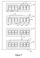
- FIG. 7 is an idealized block representation of the architecture of an arbitrary hardware device, including interconnects, which may be employed in accordance with this invention.
- FIG. 8 is a block diagram depicting a system containing a PLD prepared in accordance with this invention.
- Embodiments of the present invention will be explained in connection with various specific devices, circuits, applications, etc. herein. However, these references are for purposes of illustration only and are not intended to limit the present invention in any way. For example, one or more embodiments of the present invention will be explained using programmable logic devices (PLDs) and technologies related thereto to illustrate the present invention. However, the invention is widely applicable to other devices and in other environments. Moreover, embodiments of the present invention may be used in a wide variety of functions and/or applications.
- PLDs programmable logic devices
- a “configurable device” is a programmable device that ultimately contains user logic (that is, the function(s) programmed and implemented in a programmable device by a user, for example an electronic design).
- user logic that is, the function(s) programmed and implemented in a programmable device by a user, for example an electronic design.
- a device has a volatile memory and must be programmed upon each power-up from a non-volatile memory, though not every configurable device must possess these characteristics.
- Examples of configurable devices include SRAM PLDs and RAM-based PLDs (for example, Altera FLEX and STRATIX devices).
- a programmable device will typically include one or more large memory arrays, each having a plurality of programmable memory cells.
- the memory cells of each memory array are typically arranged so that individual cells are programmable and accessible via a plurality of word lines and bit lines.
- FIG. 1A illustrates a single RAM cell that has been programmed to a state of “0” and then left in an idle state during which both bit lines are charged to a supply voltage state of “1.” As shown, leakage current flows on path 102 through transistor P 1 and inverter 106 b during an idle state that biases both bit lines to “1.” Likewise, FIG.
- 1B illustrates the same RAM cell that has been programmed to a state of “1” and then put into an idle state with its bit lines both charged to a supply voltage state of “1.” During this idle state, leakage current flows on path 104 through transistor P 2 and inverter 106 a . The same result would occur if both bit lines were biased to “0.”
- FIG. 2 illustrates a mechanism for intelligently biasing a pair of bit lines 202 a and 202 b , which are shared by a portion of memory cells, in accordance with one embodiment of the present invention.
- the memory array portion may take any suitable form, such as a general non-volatile memory array, CRAM, SRAM, etc. Additionally, embodiments of the present invention may be implemented in any type of device that utilizes a memory array.
- An example device, in which embodiments of the present invention may be implemented, may include an FPGA device, PLD device, memory device, etc.
- bit lines 202 a and 202 b are coupled to a leakage reduction (referred herein as a configuration cognizant leakage reduction or CCLR) circuit 204 for intelligently controlling bit line bias while the memory cell portion is idle or when the bit lines are not being used for other memory access purposes.
- a leakage reduction referred herein as a configuration cognizant leakage reduction or CCLR
- a CCLR may be coupled to a single ended bit line memory cell portion.
- a CCLR is coupled with each memory array portion that shares 1 or more bit lines.
- one of the bit lines (e.g., 202 b ) and corresponding transistors (e.g., N 1 -N 7 ) would be removed.
- the CCLR receives a signal 302 that corresponds to an extra bit “Frame Bias Memory Element” for tagging the corresponding memory portion.
- This frame bias signal 302 indicates whether the corresponding memory portion has a majority of 1's or a majority of 0's.
- the frame bias signal 302 is coupled to a first multiplexer 306 a through any even number of inverters (e.g., 304 a and 304 b ), while the inverse of this frame bias signal is coupled to a second multiplexer 306 b through any odd number of inverters (e.g., 304 a ).
- the multiplexers 306 a and 306 b both receive a pre-charge signal 307 from supply 310 , for example, driven by transistor 308 .
- the CCLR circuit 300 may also include any number of amplifier buffers or transistors (not shown) to increase the signal strength of any signal or to provide impendence matching, such as for bit line signals 202 a and 202 b or mux input signals.
- bit lines may also be coupled to other circuitry (not shown), such as various multiplexers, address lines, and data lines, for causing bit values (e.g., 0 or 1) to be programmed into selected memory cells or for reading from selected memory cells.
- bit values e.g., 0 or 1
- the pre-charge transistor is also turned off for at least part of such operation.
- Embodiments of the present invention may be utilized in relation to any device that includes memory arrays.
- a programmable logic device PLD
- PLD's are integrated circuits that can be configured by a user to perform custom logic functions.
- embodiments of the present invention may be used in the context of any integrated circuit that has circuitry that can be configured by a user to perform a custom function, certain embodiments of the present invention are described in the context of programmable logic devices for clarity.
- An illustrative programmable logic device 10 in accordance with the present invention is shown in FIG. 4 .
- Programmable logic device 10 may have input/output circuitry 12 for driving signals off of device 10 and for receiving signals from other devices via input/output pins 14 .
- Pins 14 may be any suitable types of pins or solder bumps for making electrical connections between the internal circuitry of device 10 and external packaging. Some of the pins 14 may be used for high-speed communications signals. Other pins may be used to provide power supply voltages to the device 10 or may be used for DC or low-frequency signals.
- Interconnection resources 16 such as global and local vertical and horizontal conductive lines and busses may be used to route signals on device 10 .
- the remainder of the circuitry 18 on device 10 includes blocks of programmable logic, memory blocks, regions of digital signal processing circuitry, processors, hardwired circuits for supporting complex communications and arithmetic functions, etc.
- the programmable logic in circuitry 18 may include combinational and sequential logic circuitry including logic gates, multiplexers, switches, memory blocks, look-up-tables, logic arrays, etc. These illustrative components are not mutually exclusive. For example, look-up tables and other components that include logic gates and switching circuitry can be formed using multiplexers.
- the programmable logic in device 10 includes components that may be configured so that device 10 performs a desired custom logic function.
- the programmable logic in programmable logic device 10 may be based on any suitable programmable technology.
- configuration data also called programming data
- the programmable elements also sometimes called configuration bits or configuration memory
- the programmable elements may include random-access memory (RAM) cells (e.g., CRAM or SRAM) that are loaded from an external configuration device integrated circuit via certain pins 14 and appropriate portions of input/output circuitry 12 .
- RAM random-access memory
- the loaded RAM cells provide static control signals that are applied to the terminals (e.g., the gates) of circuit elements (e.g., metal-oxide-semiconductor transistors) in the programmable logic of circuitry 18 to control those elements (e.g., to turn certain transistors on or off) and thereby configure programmable logic device 10 .
- circuit elements e.g., metal-oxide-semiconductor transistors
- Circuit elements in input/output circuitry 12 and interconnection resources 16 are also generally configured by the RAM cell outputs as part of the programming process (e.g., to customize I/O and routing functions).
- the circuit elements that are configured in input/output circuitry 12 , interconnection resources 16 , and circuitry 18 may be transistors such as pass transistors or parts of multiplexers, look-up tables, logic arrays, AND, OR, NAND, and NOR logic gates, etc.
- RAM-based programmable logic device technology is merely one illustrative example of the type of technology that may be used to implement programmable logic device 10 .
- Other suitable programmable logic device technologies that may be used for device 10 include one-time programmable device arrangements such as those based on programmable logic elements made from electrically-configured fuses or electrically-configured anti-fuses, programmable logic devices in which elements 20 are formed from electrically programmable read-only-memory (EPROM) or erasable electrically-programmable read-only-memory (EEPROM) technology, or programmable logic devices with programmable elements made from magnetic storage elements, or programmable logic devices with programmable elements made from phase-change materials, etc.
- Illustrative programmable logic elements are shown schematically as elements 20 in FIG. 4 .
- the configuration memory of device 10 is preferably provided with configuration data from a user (e.g., a logic designer). Once provided with appropriate configuration data, the configuration memory will selectively control (e.g., turn on and off) portions of the circuitry in the programmable logic device 10 and thereby customize its functions so that it will operate as desired.
- a user e.g., a logic designer
- the configuration memory will selectively control (e.g., turn on and off) portions of the circuitry in the programmable logic device 10 and thereby customize its functions so that it will operate as desired.
- the circuitry of device 10 may be organized using any suitable architecture.
- the logic of programmable logic device 10 may be organized in a series of rows and columns of larger programmable logic regions or areas each of which contains multiple smaller logic regions or areas (e.g., areas of logic based on look-up tables or macrocells).
- These logic resources may be interconnected by interconnection resources 16 such as associated vertical and horizontal interconnection conductors.
- Interconnection conductors may include global conductive lines that span substantially all of device 10 , fractional lines such as half-lines or quarter lines that span part of device 10 , staggered lines of a particular length (e.g., sufficient to interconnect several logic areas), smaller local lines that interconnect small logic regions in a given portion of device 10 , or any other suitable interconnection resource arrangement.
- the logic of device 10 may be arranged in more hierarchical levels or layers in which multiple large areas are interconnected to form still larger portions of logic. Still other device arrangements may use logic that is not arranged in rows and columns. Portions of device 10 (e.g., in input/output circuitry 12 and elsewhere) may be hardwired for efficiency. As an example, hardwired wireless circuitry may be used to receive wirelessly-transmitted configuration data. Other hardwired communications circuitry and digital signal processing circuitry (e.g., multipliers, adders, etc.) may also be used.
- a programmable logic device is generally a programmable integrated circuit that allows the user of the circuit, using software control, to program the PLD to perform particular logic functions.
- PLD programmable logic device
- a wide variety of these devices are manufactured by Altera Corporation of San Jose, Calif. When an integrated circuit manufacturer supplies a typical programmable logic device, it is not yet capable of performing any specific function.
- the user in conjunction with software supplied by the manufacturer or created by the user or an affiliated source, can program the PLD to perform a particular function or functions required by the user's application.
- One or more of these programmed functions can be found in what is referred to commonly as a “core” within a PLD.
- These cores provide compartmentalized functional blocks that can be used within a programmed PLD or other logic device. Once a logic device such as a PLD is programmed with one or more of such cores, as well as any other logic as needed, the PLD can function in a larger system designed by the user just as though dedicated logic chips were employed.
- a typical design cycle may begin with a designer creating an initial block diagram and subsequently identifying any functions (IP) available for use in the anticipated system. The designer then can identify and evaluate one or more specific functions in terms of functionality and the range of parameterization available. After finding the appropriate function(s), the designer installs the function(s) into an electronic design and completes the design ( 602 ).
- IP functions
- the majority bit state for each frame may then be used to generate a frame bias value or signal for each frame, which can be used to save power after programming of the RAM as explained further herein.
- This frame bias may be stored in any suitable manner.
- the frame bias for each frame is stored as a bias bit in the particular frame's programming data.
- Assembly may include any other suitable data processing functions for analyzing and/or processing the programming data.
- assembly 608 may also include a compression operation 610 .
- the frame bias values may then be applied to each frame's bit lines in operation 618 .
- the frame biases for all of the frames are applied to such frames after all the frames are programmed.
- each frame bias value for each frame may be applied after such frame is programmed before all of the frames are programmed.
- This later embodiment would include individual enable signals (e.g., 312 of FIG. 3 ) for each frame so as to allow individual frame bias values to be applied to individual frames.
- individual enable signals may be utilized for selectively biasing bit lines of individual memory array portions for other reasons, besides programming.
- the frame bias for a particular frame is set to 1 when a majority of the bits of the frame have a 1 value.
- a bit value of 1 may correspond to a voltage or current value for a memory cell that is above a predefined memory write or read threshold value, while a 0 may corresponds to a value that is below such threshold value.
- the frame bias may be set to 0 when a majority of the bits of a frame have a 0 value. Said in another way, the value of a frame bias of a particular bit line matches the bit value of the majority value as it would be read out onto such bit line.
- the complementary bit line (if present) is set to a value that is opposite the frame bias value.
- the programmed RAM facilitates configuration of the hardware on the programmable device in order to perform their desired custom logic functions.
- the RAM may transition between a frame bias active mode and a memory or user mode (or memory activation state) in operation 620 .
- a test, error, programming, or read mode (or the like) may commence with respect to the CRAM.
- frame bias signals are deactivated (e.g., application of frame bias signals is inhibited) with respect to the bit lines.
- the frame bias mode is reactivated so that frame biases are applied to associated frame bit lines.
- Selective activation of frame bias to selected frames (or all frames) during a memory idle state will typically result in a lower number of leakage paths, as compared to techniques that pull all bit lines high during an idle state.
- a typical Sof file will contain a sparse amount of 1's, compared to the number of 0's. In other words, programming data will likely contain a clear majority (e.g., 90% 0's), as opposed to equal number of 1's and 0's. Thus, when the bias frame values correspond to majority bias values, fewer current leakage paths are formed (e.g., FIG. 2 ).
- embodiments of the present invention do not require additional voltage regulators and power rails to overdrive so as to control gate leakage. As a result, power supply size is reduced. Heat sinking requirements may also be reduced, as well as enhancing high temperature operation. Overall reliability can be increased since certain overdrive and associated stress results (e.g., oxide stress) requirements are eliminated or substantially reduced.
- CCLR embodiments require minimum circuitry for each bit line. Additionally, CCLR embodiments do not affect normal memory function and are compatible with error checking and correction processes.
- the disclosed techniques of the present invention may be implemented in any suitable combination of software and/or hardware system, such as a web-based server or desktop computer system.
- a system implementing various embodiments of the invention may be a portable device, such as a laptop or cell phone.
- the apparatus and/or web browser of this invention may be specially constructed for the required purposes, or it may be a general-purpose computer selectively activated or reconfigured by a computer program and/or data structure stored in the computer.
- the processes presented herein are not inherently related to any particular computer or other apparatus.
- various general-purpose machines may be used with programs written in accordance with the teachings herein, or it may be more convenient to construct a more specialized apparatus to perform the disclosed method steps.
- FIG. 6 illustrates a typical computer system that can be used in connection with one or more embodiments of the present invention.
- the computer system 700 includes one or more processors 702 (also referred to as central processing units, or CPUs) that are coupled to storage devices including primary storage 706 (typically a random access memory, or RAM) and another primary storage 704 (typically a read only memory, or ROM).
- primary storage 704 acts to transfer data and instructions uni-directionally to the CPU and primary storage 706 is used typically to transfer data and instructions in a bi-directional manner.
- Both of these primary storage devices may include any suitable computer-readable media described above, including a computer program product comprising a machine readable medium on which is provided program instructions according to one or more embodiments of the present invention.
- a mass storage device 708 also is coupled bi-directionally to CPU 702 and provides additional data storage capacity and may include any of the computer-readable media described above, including a computer program product comprising a machine readable medium on which is provided program instructions according to one or more embodiments of the present invention.
- the mass storage device 708 may be used to store programs, data and the like and is typically a secondary storage medium such as a hard disk that is slower than primary storage. It will be appreciated that the information retained within the mass storage device 708 , may, in appropriate cases, be incorporated in standard fashion as part of primary storage 706 as virtual memory.
- a specific mass storage device such as a CD-ROM may also pass data uni-directionally to the CPU.
- FIG. 7 This idealized representation roughly conforms to the layout of a FLEX 10K programmable logic device available from Altera Corporation of San Jose, Calif.
- a programmable logic device 800 is segmented into a plurality of “rows” to facilitate interconnection between logic elements on a given row.
- Each row of programmable logic device 800 is further subdivided into two “half-rows.”
- row 802 b is shown to contain a half-row 804 a and a half-row 804 b .
- the next lower level of the hierarchy is the “logic array block” (LAB).
- Half-row 804 b for example, contains three LABs: an LAB 806 a , an LAB 806 b , and an LAB 806 c .
- LAB 806 c includes two logic elements: a logic element 808 a and a logic element 808 b.
- PLD 800 includes four hierarchical levels: (1) rows, (2) half-rows, (3) LABs, and (4) logic elements (LEs). Any logic element within PLD 800 can be uniquely specified (and located) by specifying a value for each of these four levels of the containment hierarchy. For example, logic element 808 b can be specified as follows: row (2), half-row (2), LAB (3), LE (2).
- a synthesized netlist may be divided into logic cells (typically containing one or more gates) which are placed in the various logic elements as uniquely defined above. Thus, each logic cell from the synthesized netlist resides in a unique single logic element.
- a multi-level hardware hierarchy such as that shown in PLD 800 includes multiple levels of routing lines (interconnects). These connect the uniquely placed logic cells to complete circuits.
- interconnects interconnects
- four levels of interconnect are provided, one for each of the four hierarchy levels.
- a local interconnect such as interconnect 812 is employed to connect two logic elements within the same LAB.
- a LAB-to-LAB interconnect such as interconnect 814 is employed to connect two LABs within the same half-row.
- a “global horizontal” interconnect is employed to connect logic elements lying in the same row but in different half-rows.
- An example of a global horizontal interconnect is interconnect 816 shown in row 802 b .
- Each LAB includes eight logic elements each of which, in turn, includes a 4-input look-up table, a programmable flip-flop, and dedicated signal paths for carry and cascade functions.
- the eight logic elements in an LAB can be used to create medium-sized blocks of logic—such as 9-bit counters, address decoders, or state machines—or combined across LABs to create larger logic blocks.
- the present invention is not limited to the Altera FLEX 10K architecture or any other hardware architecture for that matter. In fact, it is not even limited to programmable logic devices. It may be employed generically in target hardware devices as broadly defined above and preferably in application specific integrated circuit designs. PLDs are just one example of ICs that can benefit from application of the present invention.
- FIG. 8 illustrates a PLD 900 of the present invention in a data processing system 902 .
- the data processing system 902 may include one or more of the following components: a processor 904 ; memory 909 ; I/O circuitry 908 ; and peripheral devices 909 . These components are coupled together by a system bus 910 and are populated on a circuit board 912 which is contained in an end-user system 914 .
- the system 902 can be used in a wide variety of applications, such as computer networking, data networking, instrumentation, video processing, digital signal processing, or any other application where the advantage of using reprogrammable logic is desirable.
- the PLD 900 can be used to perform a variety of different logic functions.
- input may be obtained using a wide variety of techniques.
- input for downloading or launching an application may be obtained via a graphical user interface from a user's interaction with a local application such as a mobile application on a mobile device, web site or web-based application or service and may be accomplished using any of a variety of well-known mechanisms for obtaining information from a user.
- a local application such as a mobile application on a mobile device, web site or web-based application or service
- machine-readable storage media that include program instructions, state information, etc. for performing various operations described herein.
- machine-readable storage media include, but are not limited to, magnetic media such as hard disks, floppy disks, and magnetic tape; optical media such as CD-ROM disks; magneto-optical media such as floptical disks; and hardware devices that are specially configured to store and perform program instructions, such as ROM and RAM.
- program instructions include both machine code, such as produced by a compiler, and files containing higher level code that may be executed by the computer using an interpreter.
Landscapes
- Engineering & Computer Science (AREA)
- Microelectronics & Electronic Packaging (AREA)
- Computer Hardware Design (AREA)
- Logic Circuits (AREA)
Abstract
Description
Claims (19)
Priority Applications (1)
| Application Number | Priority Date | Filing Date | Title |
|---|---|---|---|
| US13/605,428 US8861283B1 (en) | 2012-09-06 | 2012-09-06 | Systems and methods for reducing leakage current in memory arrays |
Applications Claiming Priority (1)
| Application Number | Priority Date | Filing Date | Title |
|---|---|---|---|
| US13/605,428 US8861283B1 (en) | 2012-09-06 | 2012-09-06 | Systems and methods for reducing leakage current in memory arrays |
Publications (1)
| Publication Number | Publication Date |
|---|---|
| US8861283B1 true US8861283B1 (en) | 2014-10-14 |
Family
ID=51661164
Family Applications (1)
| Application Number | Title | Priority Date | Filing Date |
|---|---|---|---|
| US13/605,428 Active 2032-11-03 US8861283B1 (en) | 2012-09-06 | 2012-09-06 | Systems and methods for reducing leakage current in memory arrays |
Country Status (1)
| Country | Link |
|---|---|
| US (1) | US8861283B1 (en) |
Cited By (1)
| Publication number | Priority date | Publication date | Assignee | Title |
|---|---|---|---|---|
| US20230133665A1 (en) * | 2020-05-28 | 2023-05-04 | Inspur Electronic Information Industry Co., Ltd. | Data storage method, apparatus, and device, and readable storage medium |
Citations (3)
| Publication number | Priority date | Publication date | Assignee | Title |
|---|---|---|---|---|
| US20050018519A1 (en) * | 2003-07-24 | 2005-01-27 | Renesas Technology Corp. | Semiconductor memory device capable of reducing power consumption during reading and standby |
| US20080273402A1 (en) * | 2007-05-04 | 2008-11-06 | International Business Machines Corporation | Apparatus for implementing domino sram leakage current reduction |
| US20110063895A1 (en) * | 2009-09-14 | 2011-03-17 | Renesas Electronics Corporation | Semiconductor integrated circuit device and system |
-
2012
- 2012-09-06 US US13/605,428 patent/US8861283B1/en active Active
Patent Citations (3)
| Publication number | Priority date | Publication date | Assignee | Title |
|---|---|---|---|---|
| US20050018519A1 (en) * | 2003-07-24 | 2005-01-27 | Renesas Technology Corp. | Semiconductor memory device capable of reducing power consumption during reading and standby |
| US20080273402A1 (en) * | 2007-05-04 | 2008-11-06 | International Business Machines Corporation | Apparatus for implementing domino sram leakage current reduction |
| US20110063895A1 (en) * | 2009-09-14 | 2011-03-17 | Renesas Electronics Corporation | Semiconductor integrated circuit device and system |
Cited By (2)
| Publication number | Priority date | Publication date | Assignee | Title |
|---|---|---|---|---|
| US20230133665A1 (en) * | 2020-05-28 | 2023-05-04 | Inspur Electronic Information Industry Co., Ltd. | Data storage method, apparatus, and device, and readable storage medium |
| US11698730B2 (en) * | 2020-05-28 | 2023-07-11 | Inspur Electronic Information Industry Co., Ltd. | Data storage method, apparatus, and device, and readable storage medium |
Similar Documents
| Publication | Publication Date | Title |
|---|---|---|
| US7675317B2 (en) | Integrated circuits with adjustable body bias and power supply circuitry | |
| US8072237B1 (en) | Computer-aided design tools and memory element power supply circuitry for selectively overdriving circuit blocks | |
| US20190018063A1 (en) | Programmable integrated circuits with in-operation reconfiguration capability | |
| EP2728753B1 (en) | Programmable integrated circuits with redundant circuitry | |
| US7463057B1 (en) | Integrated circuits with adjustable memory element power supplies | |
| US8612814B1 (en) | Memory error detection circuitry | |
| US9455715B2 (en) | Apparatus for improving reliability of electronic circuitry and associated methods | |
| US20140021981A1 (en) | Integrated circuits with logic regions having input and output bypass paths for accessing registers | |
| US20210383049A1 (en) | Methods and apparatus for reducing reliability degradation on an integrated circuit | |
| CN101529374B (en) | For the volatile memory elements with boosted output voltages of programmable logic device integrated circuits | |
| US9098486B1 (en) | Methods and apparatus for testing multiple clock domain memories | |
| US9230048B1 (en) | Integrated circuits with interconnect selection circuitry | |
| US9601217B1 (en) | Methods and circuitry for identifying logic regions affected by soft errors | |
| US10235485B1 (en) | Partial reconfiguration debugging using hybrid models | |
| US7417918B1 (en) | Method and apparatus for configuring the operating speed of a programmable logic device through a self-timed reference circuit | |
| US7107566B1 (en) | Programmable logic device design tools with gate leakage reduction capabilities | |
| US10229748B1 (en) | Memory interface latch with integrated write-through function | |
| US8861283B1 (en) | Systems and methods for reducing leakage current in memory arrays | |
| US10152566B1 (en) | Constraint based bit-stream compression in hardware for programmable devices | |
| US11017138B2 (en) | Timing analysis for parallel multi-state driver circuits | |
| US9607671B1 (en) | Programmable integrated circuits with in-operation reconfiguration capability | |
| US10916323B2 (en) | Memory interface latch with integrated write-through and fence functions | |
| CN117236254A (en) | Configurable logic block control method, configurable logic block and storage medium | |
| US7319619B1 (en) | Programmable logic device memory blocks with adjustable timing | |
| US7444613B1 (en) | Systems and methods for mapping arbitrary logic functions into synchronous embedded memories |
Legal Events
| Date | Code | Title | Description |
|---|---|---|---|
| AS | Assignment |
Owner name: ALTERA CORPORATION, CALIFORNIA Free format text: ASSIGNMENT OF ASSIGNORS INTEREST;ASSIGNORS:WONG, BRIAN YUNG FAN;SINHA, SHANKAR;LEE, SHIH-LIN S.;AND OTHERS;SIGNING DATES FROM 20120823 TO 20120828;REEL/FRAME:028933/0375 |
|
| AS | Assignment |
Owner name: ALTERA CORPORATION, CALIFORNIA Free format text: CORRECTIVE ASSIGNMENT TO CORRECT THE ASSIGNOR NAME PREVIOUSLY RECORDED AT REEL: 028933 FRAME: 0375. ASSIGNOR(S) HEREBY CONFIRMS THE ASSIGNMENT;ASSIGNORS:WONG, BRIAN YUNG FUN;SINHA, SHANKAR;LEE, SHIH-LIN S.;AND OTHERS;SIGNING DATES FROM 20120823 TO 20120828;REEL/FRAME:033647/0485 |
|
| STCF | Information on status: patent grant |
Free format text: PATENTED CASE |
|
| MAFP | Maintenance fee payment |
Free format text: PAYMENT OF MAINTENANCE FEE, 4TH YEAR, LARGE ENTITY (ORIGINAL EVENT CODE: M1551) Year of fee payment: 4 |
|
| MAFP | Maintenance fee payment |
Free format text: PAYMENT OF MAINTENANCE FEE, 8TH YEAR, LARGE ENTITY (ORIGINAL EVENT CODE: M1552); ENTITY STATUS OF PATENT OWNER: LARGE ENTITY Year of fee payment: 8 |
|
| AS | Assignment |
Owner name: BARCLAYS BANK PLC, AS COLLATERAL AGENT, NEW JERSEY Free format text: SECURITY INTEREST;ASSIGNOR:ALTERA CORPORATION;REEL/FRAME:073431/0309 Effective date: 20250912 |
|
| MAFP | Maintenance fee payment |
Free format text: PAYMENT OF MAINTENANCE FEE, 12TH YEAR, LARGE ENTITY (ORIGINAL EVENT CODE: M1553); ENTITY STATUS OF PATENT OWNER: LARGE ENTITY Year of fee payment: 12 |