US8860658B2 - Electrophoretic display unit and method for driving an electrophoretic display panel - Google Patents
Electrophoretic display unit and method for driving an electrophoretic display panel Download PDFInfo
- Publication number
- US8860658B2 US8860658B2 US12/781,698 US78169810A US8860658B2 US 8860658 B2 US8860658 B2 US 8860658B2 US 78169810 A US78169810 A US 78169810A US 8860658 B2 US8860658 B2 US 8860658B2
- Authority
- US
- United States
- Prior art keywords
- sensor
- electrode
- resistance
- electrophoretic display
- area
- Prior art date
- Legal status (The legal status is an assumption and is not a legal conclusion. Google has not performed a legal analysis and makes no representation as to the accuracy of the status listed.)
- Expired - Fee Related, expires
Links
Images


Classifications
-
- G—PHYSICS
- G02—OPTICS
- G02F—OPTICAL DEVICES OR ARRANGEMENTS FOR THE CONTROL OF LIGHT BY MODIFICATION OF THE OPTICAL PROPERTIES OF THE MEDIA OF THE ELEMENTS INVOLVED THEREIN; NON-LINEAR OPTICS; FREQUENCY-CHANGING OF LIGHT; OPTICAL LOGIC ELEMENTS; OPTICAL ANALOGUE/DIGITAL CONVERTERS
- G02F1/00—Devices or arrangements for the control of the intensity, colour, phase, polarisation or direction of light arriving from an independent light source, e.g. switching, gating or modulating; Non-linear optics
- G02F1/01—Devices or arrangements for the control of the intensity, colour, phase, polarisation or direction of light arriving from an independent light source, e.g. switching, gating or modulating; Non-linear optics for the control of the intensity, phase, polarisation or colour
- G02F1/165—Devices or arrangements for the control of the intensity, colour, phase, polarisation or direction of light arriving from an independent light source, e.g. switching, gating or modulating; Non-linear optics for the control of the intensity, phase, polarisation or colour based on translational movement of particles in a fluid under the influence of an applied field
- G02F1/166—Devices or arrangements for the control of the intensity, colour, phase, polarisation or direction of light arriving from an independent light source, e.g. switching, gating or modulating; Non-linear optics for the control of the intensity, phase, polarisation or colour based on translational movement of particles in a fluid under the influence of an applied field characterised by the electro-optical or magneto-optical effect
- G02F1/167—Devices or arrangements for the control of the intensity, colour, phase, polarisation or direction of light arriving from an independent light source, e.g. switching, gating or modulating; Non-linear optics for the control of the intensity, phase, polarisation or colour based on translational movement of particles in a fluid under the influence of an applied field characterised by the electro-optical or magneto-optical effect by electrophoresis
-
- G—PHYSICS
- G09—EDUCATION; CRYPTOGRAPHY; DISPLAY; ADVERTISING; SEALS
- G09G—ARRANGEMENTS OR CIRCUITS FOR CONTROL OF INDICATING DEVICES USING STATIC MEANS TO PRESENT VARIABLE INFORMATION
- G09G3/00—Control arrangements or circuits, of interest only in connection with visual indicators other than cathode-ray tubes
- G09G3/20—Control arrangements or circuits, of interest only in connection with visual indicators other than cathode-ray tubes for presentation of an assembly of a number of characters, e.g. a page, by composing the assembly by combination of individual elements arranged in a matrix no fixed position being assigned to or needed to be assigned to the individual characters or partial characters
- G09G3/34—Control arrangements or circuits, of interest only in connection with visual indicators other than cathode-ray tubes for presentation of an assembly of a number of characters, e.g. a page, by composing the assembly by combination of individual elements arranged in a matrix no fixed position being assigned to or needed to be assigned to the individual characters or partial characters by control of light from an independent source
- G09G3/3433—Control arrangements or circuits, of interest only in connection with visual indicators other than cathode-ray tubes for presentation of an assembly of a number of characters, e.g. a page, by composing the assembly by combination of individual elements arranged in a matrix no fixed position being assigned to or needed to be assigned to the individual characters or partial characters by control of light from an independent source using light modulating elements actuated by an electric field and being other than liquid crystal devices and electrochromic devices
- G09G3/344—Control arrangements or circuits, of interest only in connection with visual indicators other than cathode-ray tubes for presentation of an assembly of a number of characters, e.g. a page, by composing the assembly by combination of individual elements arranged in a matrix no fixed position being assigned to or needed to be assigned to the individual characters or partial characters by control of light from an independent source using light modulating elements actuated by an electric field and being other than liquid crystal devices and electrochromic devices based on particles moving in a fluid or in a gas, e.g. electrophoretic devices
-
- G—PHYSICS
- G09—EDUCATION; CRYPTOGRAPHY; DISPLAY; ADVERTISING; SEALS
- G09G—ARRANGEMENTS OR CIRCUITS FOR CONTROL OF INDICATING DEVICES USING STATIC MEANS TO PRESENT VARIABLE INFORMATION
- G09G2300/00—Aspects of the constitution of display devices
- G09G2300/08—Active matrix structure, i.e. with use of active elements, inclusive of non-linear two terminal elements, in the pixels together with light emitting or modulating elements
-
- G—PHYSICS
- G09—EDUCATION; CRYPTOGRAPHY; DISPLAY; ADVERTISING; SEALS
- G09G—ARRANGEMENTS OR CIRCUITS FOR CONTROL OF INDICATING DEVICES USING STATIC MEANS TO PRESENT VARIABLE INFORMATION
- G09G2320/00—Control of display operating conditions
- G09G2320/04—Maintaining the quality of display appearance
- G09G2320/041—Temperature compensation
Definitions
- the present invention relates to electrophoretic display units, and to methods of driving an electrophoretic display panel.
- An electrophoretic display panel that comprises a plurality of electrophoretic display elements arranged between a first electrode layer and second electrode layer.
- the display elements are capsules with a dispersion of electrically charged black and white or colored nano-particles in a clear solution.
- the display panel may be manufactured by depositing an emulsion of these capsules in an appropriate binder as a dense monolayer onto an organic substrate with an electrode of an electrically conductive, transparent material, such as indium tin oxide (ITO). After that, the binder is cured to make the system mechanically robust.
- the electrophoretic medium so obtained is laminated by a thin adhesive layer onto a backplane, thereby sandwiching the capsules, binder and adhesive between the ITO electrode and the backplane electrodes (e.g. pixel pads of an active-matrix display).
- the black and white particles are moved within the capsules by applying an electric field between the ITO and backplane electrode, thereby enabling rendering of grey levels.
- the behavior of the display panel is influenced by its temperature in several ways.
- the viscosity of the capsule fluid, and therewith the mobility of the nano-particles, is dependent on the temperature.
- the display elements are arranged as an active matrix, the behavior of the transistor elements of the active matrix is dependent on temperature.
- the electric behavior mainly resistance, further denoted herein as cell gap resistance or briefly CGR
- the binder, capsule walls and adhesive layer will change dramatically with changing temperature. Generally these effects will cause the switching speed to increase with increasing temperature. Care has to be taken however that the decreasing resistance between the ITO and the backplane electrode does not cause the switching behavior to degenerate. This will cause sub-optimal driving and thereby visible artifacts such as ghosting, image sticking or deviations in grey scale rendering.
- a rollable display in its rolled out state adapts very fast to the temperature in the environment as it is extremely thin and lightweight.
- US2007/0052665 A1 describes an electrophoretic display unit that is provided with an embedded temperature sensor embedded in the display panel, typically a silicon based sensor.
- the sensor or other temperature sensing device equipped with a transducer transmits a digital control signal to a processor.
- the processor uses this digital control signal to drive the display elements with a progressive number of pre-pulses at higher temperatures.
- an electrophoretic display unit that includes:
- an electrophoretic display panel comprising a medium having embedded therein a plurality of electrophoretic display elements controlled by a first and a second pixel electrode,
- a sensor constructed to generate a signal dependent on a temperature of the display panel
- the sensor includes a resistance sensor constructed to detect a resistance of the medium between a first and a second sensor electrode, and the driver is controllable according to the resistance detected by the resistance sensor.
- the cell gap resistance of the medium varies as a function of temperature.
- this effect is used to compensate the behavior of the display panel for temperature changes.
- the temperature or the value for a suitable control signal can be determined using a formula or look-up table. Because cell gap resistance is the most important factor influencing the driving characteristics of the display, measuring this parameter is the most direct way to determine a driving scheme that compensates for this effect.
- Characteristics of the driver may further be controlled by other signals, for example, the type of content, application, image (meta) data etc.
- the medium is sandwiched between a first and a second electrode layer.
- the sensor electrodes may be formed as separate elements arranged in the medium between the first and the second electrode layer.
- the first and the second sensor electrode are formed by the first and the second electrode layer respectively. This is advantageous in that the sensor electrodes can be manufactured with the display electrodes in the same processing steps.
- An electrode may be used as a sensor electrode and as a pixel electrode on a time-multiplexed basis.
- an electrode may simultaneously serve as a pixel electrode and as a sensor electrode by superposing a measurement signal for measuring the cell gap resistance onto the drive signal for controlling one or more display elements.
- at least one of the sensor electrodes is a separate portion within one of the electrode layers. This simplifies the control of the display elements and the measurement of the cell gap resistance.
- the other sensor electrode may be integral with the other of the electrode layers.
- first and the second electrode layer may each comprise a plurality of electrode lines, wherein the electrode lines of the first electrode layer are arranged transverse to the electrode lines of the second electrode layer.
- the display elements are driven segment-wise by a plurality of segment electrodes, each controlling a respective segment with one or more display elements.
- Each segment electrode may have a corresponding counter electrode.
- the segment electrodes may have a common counter electrode.
- the segment electrodes may be each controlled by a respective drive element, for example a switching element, such as a transistor.
- the first electrode layer comprises individual electrode portions, wherein one of said electrode portions forms the first sensor electrode of the at least one sensor and the second electrode layer comprises a common electrode that also forms the second sensor electrode of the at least one sensor.
- This arrangement is favorable for use in an active-matrix display.
- the resistance measured in this embodiment is substantially the resistance of the medium atop the first sensor electrode.
- the electrophoretic display unit may have a plurality of sensors, wherein each sensor has a resistance sensor with a respective electrode portion in the first electrode layer.
- One or more individual electrode portions of the first electrode layer may serve both as first sensor electrodes and as display electrodes. Such individual electrode portions may be alternatively switched to measure a resistance of the medium in their neighborhood and as a display electrode to control the electrophoretic display elements.
- one or more individual electrode portions in the first electrode layer are dedicated as sensor electrodes. In this way interference between the display function and the sensor function is avoided.
- the electrophoretic display panel may have a central display area with individual electrode portions controlled by a matrix of transistor elements and one or more electrode portions added around the display area to measure a resistance of the medium between said electrode portions and the opposing common electrode.
- the sensors corresponding to each of the sensor electrodes may each generate a respective temperature dependent signal (temperature signal).
- the set of temperature signals generated in this way may be used to generate an overall temperature signal that is representative for an average temperature of the display panel.
- the temperature signals may be used to control the driving scheme of respective sections in the central area of the display panel.
- Two or more temperature signals may be interpolated to generate an interpolated temperature signal that is representative for a temperature at a specific location at the central area.
- the senor is part of a sensor unit that further comprises a drive module that provides a predetermined electric signal to the sensor electrodes and a measurement module that measures a parameter of said electric signal depending on the resistive value of the resistance.
- the predetermined signal is for example a square wave signal having an amplitude of a predetermined voltage.
- the predetermined signal may also be a DC signal.
- the measurement module may measure the current flowing through the resistance.
- the predetermined electrical signal may be a current with a predetermined amplitude. In that case the measurement module may measure the voltage over the resistance.
- the frequency of the predetermined electric signal is preferably in a range of 10 Hz to 1 MHz. If the frequency is significantly lower than 10 Hz, e.g. 5 Hz, the display elements involved in the measurement will show a visual effect. If the frequency is significantly higher than 1 MHz, e.g. 10 MHz, then the accuracy of the measurement may be relatively low.
- the senor is part of a sensor unit that further comprises an oscillator circuit that generates an electric signal with a frequency dependent on a resistive value of the resistance between the sensor electrodes.
- the output signal representing the cell-gap resistance does not need an A/D-converter to be acquired by a fully digital controller.
- Pulse-width and frequency are very well suited to be measured by fully digital circuitry. By means of a look-up table, these values can be mapped to generate values of a signal for effectively compensating temperature dependent behavior of the display panel.
- the frequency of the predetermined electric signal is preferably in a range of 10 Hz to 1 MHz.
- the oscillator circuit may be designed such that within normal temperature ranges the frequency remains within the above-mentioned boundaries of 10 Hz and 1 MHz.
- a portion of the display panel that comprises the resistance sensor may be provided with a non-transparent layer, so that fluctuations of the state of the display elements due to the measurement are not visible also at lower frequencies.
- the medium may be free of display elements near the sensor electrodes.
- the temperature compensation scheme it has to be taken into account that the resistance of the medium measured in front of said sensor electrodes differs from the resistance of the medium in the display area.
- the sensor electrodes are both located in the display panel, with the display medium in front of the sensor electrodes, and the resistance measured by the sensor is not the cell gap resistance but a lateral resistance.
- This lateral resistance that is measured has a one-to-one relation to the cell gap resistance.
- a method for driving an electrophoretic display panel comprising the steps of
- An option is to increase the amplitude of the drive signal for driving the display elements to compensate a tendency of the display panel to react more slowly at lower temperatures.
- Another option is to increase the width of drive signal pulses for driving the display elements to compensate a tendency of the display panel to react more slowly at lower temperatures.
- Yet another option is to add a number of pre-pulses with a progressively shorter duration at higher temperatures to the drive signal for driving the display elements, as is described in the above-mentioned prior art US2007/0052665.
- FIG. 1 schematically shows an electrophoretic display unit having a display panel
- FIG. 2 is an equivalent circuit diagram of a portion of the display panel
- FIG. 3 is a cross-section according to III-III in FIG. 1 ,
- FIG. 4 shows a relation measured between a resistance of an electrophoretic medium and a temperature thereof
- FIG. 5 shows the sensor unit in a first embodiment of the display unit
- FIG. 5A shows electric signals occurring in the sensor unit of FIG. 5 .
- FIG. 6 shows the sensor unit in a second embodiment of the display unit
- FIG. 6A shows an electric model of a part of the display unit
- FIG. 6B shows electric signals occurring in the sensor unit of FIG. 6 .
- FIG. 6C shows an alternative sensor unit in the second embodiment of the display unit
- FIG. 7 shows a geometrical arrangement of various parts in a practical embodiment of the display unit
- FIG. 7A shows a detail according to VIIA in FIG. 7 .
- Embodiments of the invention are described herein with reference to cross-section illustrations that are schematic illustrations of idealized embodiments (and intermediate structures) of the invention. As such, variations from the shapes of the illustrations as a result, for example, of manufacturing techniques and/or tolerances, are to be expected. Thus, embodiments of the invention should not be construed as limited to the particular shapes and sizes of regions illustrated herein but are to include deviations in shapes that result, for example, from manufacturing.
- FIG. 1 schematically shows an electrophoretic display unit that comprises an electrophoretic display panel 1 , a driver 15 for driving the display panel 1 and a sensor unit 25 .
- the display panel 1 is an active matrix display.
- FIG. 2 is an equivalent circuit diagram of a portion of the display panel 1
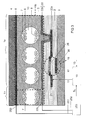
- FIG. 3 shows a cross-section according to III-III in FIG. 1 .
- the display panel 1 comprises an electrophoretic medium 5 having embedded electrophoretic display elements 7 between electrode 6 on top substrate 4 and electrode 22 on substrate 3 provided with active switching elements 19 .
- FIG. 3 only shows a single switching element 19 and associated pixel 18 .
- the display panel 1 may have a plurality of switching elements arranged in a matrix comprising several hundreds to several thousands of rows and several hundreds to several thousands of columns.
- the active switching element 19 is a thin film transistor with gate electrode 20 , semiconducting channel 26 , source electrode 21 and drain electrode 22 a that is electrically coupled to the pixel electrode 22 b of the associated pixel 18 .
- the pixel 18 controlled by the active switching element 19 comprises a set of display elements in the form of microcapsules 7 embedded in the medium 5 .
- a counter electrode 6 is provided on the film comprising the encapsulated electrophoretic ink, but a counter electrode could be alternatively provided too on the base substrate in the case of operation with in-plane electric fields.
- the set of display elements 7 may comprise one or more display elements.
- the electrophoretic medium with the embedded electrophoretic display elements 7 is arranged between a first electrode layer 22 and a second electrode layer 6 . At least one of the electrode layers 6 , 22 , here the first electrode layer 22 has a plurality of mutually separate electrode portions 22 b , 22 c .
- the display elements 7 are formed by microcapsules that comprise a dispersion of positively charged white nano-particles 8 and negatively charged black nano-particles 9 in a clear solution 10 .
- the medium 5 is preferably a transparent polymeric material that may be cured (i.e., cross-linked from a low-viscosity state into extremely high viscosity) or otherwise solidified at relatively low temperatures, and which readily accepts, in its low-viscosity state, a dispersion of microcapsules.
- Useful materials include polyvinyl alcohols, gelatins, epoxies and other resins.
- the driver 15 for driving the active switching elements 19 comprises a row driver 16 and a column driver 10 and a processor 150 that controls the row and column driver 16 , 10 .
- the display panel 1 comprises a matrix of display elements at the area of crossings of row or selection electrodes 17 and column or data electrodes 11 .
- the row driver 16 consecutively selects the row electrodes 17
- a column driver 10 provides a data signal to the column electrodes 11 .
- the processor 150 first processes incoming data 13 , including input from the sensor unit 25 into the data signals, in particular, the (pre)pulses and (pre)pulse sequence of the present invention.
- Counter electrodes may be coupled to two outputs 85 , 87 of the processor 150 .
- the display device of FIG. 1 also comprises an additional capacitor 23 at the location of each display element 18 .
- the additional capacitor 23 is connected to one or more storage capacitor lines 24 .
- TFT's other switching elements can be used, such as diodes, MIM's, etc.
- the sensor unit 25 has a resistance sensor 250 that is embedded in the display panel 1 .
- the sensor unit 25 generates a dependent signal, in the sequel also denoted as temperature signal S T that is indicative for a temperature of the display panel 1 .
- the at least one sensor unit 25 generates the temperature signal S T dependent on the resistance of the medium 5 between a first sensor electrode 22 c and a second sensor electrode 6 .
- the first sensor electrode 22 c , the second sensor electrode 6 and the medium 5 between the first and the second sensor electrode 22 c , 6 forms the resistance sensor 250 .
- the resistance measured between the first and the second sensor electrode 22 c , 6 is substantially the resistance of the portion of the medium 5 that is present atop the first sensor electrode 6 .
- the resistance sensor 250 is coupled via signal lines 251 , 252 to signal generation unit 253 that generates the temperature signal S T .
- the driver 15 for driving the display panel 1 has a characteristic that is controlled by the temperature signal S T of the at least one sensor unit 25 .
- the first sensor electrode 22 c and the second sensor electrode 6 are formed by the first electrode layer 22 and the second electrode layer 6 respectively.
- the first electrode layer 22 comprises individual electrode portions 22 b , 22 c .
- One of the electrode portions forms the first sensor electrode 22 c of the at least one sensor unit 25 .
- the second electrode layer 6 comprises a common electrode that also forms the second sensor electrode 6 of the at least one sensor unit 25 .
- the second electrode layer 6 also functions as a common electrode for the display elements 7 .
- the individual electrode portion 22 c in the first electrode layer 22 is dedicated as a sensor electrode. It has no function for display purposes.
- the electrophoretic display panel 1 has a central display area 1 a with individual electrode portions 22 b forming pixel electrodes.
- the pixel electrodes 22 b are controlled by a matrix of transistor elements 19 via a respective drain 22 a thereof.
- the display panel 1 further has one or more electrode portions 22 c in an area 1 b outside the display area 1 a to measure a resistance of the medium 5 between said sensor electrode formed by portion 22 c and the opposing common electrode 6 .
- the area 1 b is a border around the display area 1 a . The measurements may be carried out during periodically recurring time intervals.
- a control voltage may be applied at the sensor electrodes 22 c , 6 to achieve that the border assumes a predetermined gray-value or color for decorative purposes.
- the electrode portion 22 c may cover the entire border 1 b , so that the resistance measured is the average value of the resistance of the medium 5 present in the medium between the substrates 3 and 4 in the border region.
- the border 1 b may comprise a plurality of mutually separate electrode portions of respective mutually independent resistance sensors. In that case a temperature may be estimated for each of various regions of the display panel.
- FIG. 4 shows the relation between cell gap resistance R in M ⁇ cm 2 and temperature T in 0° C. as measured for various species of a regular E Ink VizplexTM laminate.
- the cell gap resistance is in the order of 50M ⁇ cm 2 at room temperature. It varies between 5M ⁇ cm 2 at high temperatures (50° C.) to >100M ⁇ cm 2 at low temperatures (0° C.).
- the total area of the border electrode is about 2 cm 2 , necessitating a resistance measurement with a range of 1 . . . 100M ⁇ .
- the temperature T was varied between 0 and 50 degrees. In a range of 10 to 50 degrees the resistance of the medium is a good indicator of the temperature.
- the variation of the cell gap resistance (CGR) within a batch is smaller than ⁇ 5%, and within a batch the shape of the temperature dependence is identical for all samples. Accordingly a lookup table (LUT) for determining the temperature as a function of the cell gap resistance may be based on measurements for a single sample.
- the dependence of the cell gap resistance on the temperature is in practice the most important cause for the temperature behavior of the display panel. Due to its high sensitivity it is also a very good indicator for the environment temperature. Also for this reason the cell gap resistance itself instead of the temperature can be monitored and used as the parameter that indicates the expected behavior of the display panel.
- FIG. 5 shows a signal generation unit 253 in a first embodiment of the display unit.
- the signal generation unit 253 comprises a drive module 254 that provides a predetermined electric signal to the sensor electrodes of the sensor 250 and a measurement module 255 that measures a parameter of said electric signal depending on the resistive value of the resistance.
- a signal is applied having a voltage that periodically alternates between U 1 , U 2 , U 3 (as shown in FIG. 5A ) and the current I through the sensor 250 with the cell gap resistance is measured after steady state is attained to exclude capacitive effects.
- the current may be varied according to a predetermined pattern by a current source and the resulting voltage over the cell gap resistance may be measured.
- the signal generation circuit 253 of the at least one sensor unit 25 comprises an oscillator circuit 256 that includes the resistance sensor 250 and that generates an electric signal V OUT with a frequency dependent on a resistive value of the resistance sensor 250 .
- the oscillator circuit 256 comprises an op-amp IC 1 , e.g. of type TLV271 DBV having an output 1 , a non-inverting input 3 and an inverting input 4 .
- the non-inverting input 3 is coupled to a central node of a first voltage divider that comprises a first and a second resistor R 1 , R 2 each of 100 k ⁇ and that is connected at one end to ground (GND) and at the other end to VDD, here having a value of 3V.
- the oscillator circuit 256 comprises a second voltage divider R 5 , R 6 having a first and a second resistor R 5 , R 6 , each of 10 k ⁇ .
- the inverting input 4 of the op-amp IC 1 is coupled to the central node of the second voltage divider R 5 , R 6 via the resistance sensor 250 .
- the non-inverting input 3 of the op-amp IC 1 is further coupled to the output 1 via a feedback resistor R 3 of 100 k ⁇ .
- the inverting input 4 of the op-amp IC 1 is further coupled to the output 1 via a feedback resistor R 4 of 10M ⁇ .
- FIG. 6A shows a model of the electric behavior of the medium 5 including the electrophoretic display elements.
- the electric behavior is modelled as a capacitive element C 1 in parallel to a series arrangement of a resistive element R 7 and a voltage source G 1 .
- the voltage source G 1 models the charge accumulation behavior of the medium 5 .
- FIG. 6B shows electric signals occurring in the oscillator circuit 256 of FIG. 6 .
- the inner curve shows the voltage ⁇ V over the input terminals of the operational amplifier IC 1
- the outer curve shows the temperature signal V OUT at the output of the oscillator circuit 256 . Due to the high amplification of the operational amplifier IC 1 , the output signal V OUT saturates to a rectangular wave.
- the output signal V OUT so obtained can be directly processed further by digital circuitry into a temperature signal S T .
- the digital circuitry 257 preferably comprises a digital frequency or pulse width measurement circuit and a lookup table for determining a value for the temperature signal S T as a function of the measured value of the frequency or pulse width. Digital measurement of a frequency or pulse width is relatively simple.
- FIG. 6C shows an alternative embodiment of the oscillator circuit 256 .
- the embodiment shown therein differs from the one of FIG. 6 , in that the first input 3 of the operational amplifier is coupled via a resistive element R 8 , in this case having a resistive value of 50K ⁇ to ground GND, instead of to a central node of a voltage divider.
- the resistance sensor 250 that measures the cell gap resistance CGR is coupled to ground GND, here via a resistor R 12 having a resistive value of 50K ⁇ , instead of to a central node of a voltage divider.
- a single supply voltage suffices.
- the circuit of FIG. 6C is simpler, but needs a set of 2 symmetric supply voltages.
- FIG. 7 shows an example how various parts of the display unit may be geometrically arranged.
- FIG. 7A shows a detail VIIA of FIG. 7 .
- the embodiment shown in FIG. 7 has separate column drivers 10 a , 10 b for driving a first half 11 a and a second half 11 b of the column electrodes 11 and a row driver 16 for driving the row electrodes 17 .
- the row driver 16 and the column drivers 10 a , 10 b are controlled by processor 150 .
- circuitry 25 for determining the temperature signal ST from a value measured for the cell gap resistance CGR.
- FIG. 7A it can be seen that the display 1 has a central area 1 a for display purposes and a border area 1 b for measurement purposes.
- the border area 1 b comprises a first and a second sensor electrode. One thereof, here electrode is separate from the pixel electrodes. The other sensor electrode may also be separate, but that is not necessary.
- the border 1 b may also be used to visually frame the central area 1 a of the display with a controllable gray-value or color.
Landscapes
- Physics & Mathematics (AREA)
- Engineering & Computer Science (AREA)
- General Physics & Mathematics (AREA)
- Nonlinear Science (AREA)
- Chemical Kinetics & Catalysis (AREA)
- Molecular Biology (AREA)
- Electrochemistry (AREA)
- Health & Medical Sciences (AREA)
- Chemical & Material Sciences (AREA)
- Optics & Photonics (AREA)
- Life Sciences & Earth Sciences (AREA)
- Computer Hardware Design (AREA)
- Theoretical Computer Science (AREA)
- Electrochromic Elements, Electrophoresis, Or Variable Reflection Or Absorption Elements (AREA)
- Control Of Indicators Other Than Cathode Ray Tubes (AREA)
Abstract
Description
Claims (5)
Priority Applications (4)
| Application Number | Priority Date | Filing Date | Title |
|---|---|---|---|
| US12/781,698 US8860658B2 (en) | 2010-05-17 | 2010-05-17 | Electrophoretic display unit and method for driving an electrophoretic display panel |
| EP11720898.3A EP2572238B1 (en) | 2010-05-17 | 2011-05-16 | Electrophoretic display unit and method for driving an electrophoretic display panel |
| CN2011800248730A CN102906637A (en) | 2010-05-17 | 2011-05-16 | Electrophoretic display unit and method for driving electrophoretic display panel |
| PCT/NL2011/050331 WO2011145932A1 (en) | 2010-05-17 | 2011-05-16 | Electrophoretic display unit and method for driving an electrophoretic display panel |
Applications Claiming Priority (1)
| Application Number | Priority Date | Filing Date | Title |
|---|---|---|---|
| US12/781,698 US8860658B2 (en) | 2010-05-17 | 2010-05-17 | Electrophoretic display unit and method for driving an electrophoretic display panel |
Publications (2)
| Publication Number | Publication Date |
|---|---|
| US20110279442A1 US20110279442A1 (en) | 2011-11-17 |
| US8860658B2 true US8860658B2 (en) | 2014-10-14 |
Family
ID=44343195
Family Applications (1)
| Application Number | Title | Priority Date | Filing Date |
|---|---|---|---|
| US12/781,698 Expired - Fee Related US8860658B2 (en) | 2010-05-17 | 2010-05-17 | Electrophoretic display unit and method for driving an electrophoretic display panel |
Country Status (4)
| Country | Link |
|---|---|
| US (1) | US8860658B2 (en) |
| EP (1) | EP2572238B1 (en) |
| CN (1) | CN102906637A (en) |
| WO (1) | WO2011145932A1 (en) |
Cited By (2)
| Publication number | Priority date | Publication date | Assignee | Title |
|---|---|---|---|---|
| US20150109658A1 (en) * | 2013-10-18 | 2015-04-23 | E Ink Holdings Inc. | Electrophoretic display apparatus |
| TWI664482B (en) * | 2018-01-05 | 2019-07-01 | 元太科技工業股份有限公司 | Electrophoretic display and driving method thereof |
Families Citing this family (27)
| Publication number | Priority date | Publication date | Assignee | Title |
|---|---|---|---|---|
| KR101712544B1 (en) * | 2010-08-17 | 2017-03-07 | 삼성디스플레이 주식회사 | Electro phoretic indication display |
| TWI449012B (en) * | 2012-04-20 | 2014-08-11 | E Ink Holdings Inc | Display apparatus and display method thereof |
| CN103377606A (en) * | 2012-04-25 | 2013-10-30 | 联咏科技股份有限公司 | Display panel temperature sensing device |
| JP2013250475A (en) * | 2012-06-01 | 2013-12-12 | Sony Corp | Display control apparatus, display control method, program and recording medium |
| TWI460701B (en) * | 2012-06-11 | 2014-11-11 | Univ Nat Taiwan Normal | System and method for driving an electrophoretic display of reference image stay time |
| US9939706B2 (en) | 2013-03-26 | 2018-04-10 | Clearink Displays, Inc. | Displaced porous electrode for frustrating TIR and returning light through exit pupil |
| WO2014189751A1 (en) | 2013-05-22 | 2014-11-27 | Clearink Displays Llc | Method and apparatus for improved color filter saturation |
| JP6360557B2 (en) | 2013-07-08 | 2018-07-18 | クリアインク ディスプレイズ, インコーポレイテッドClearink Displays, Inc. | TIR-modulated wide viewing angle display |
| CN105659310B (en) | 2013-08-13 | 2021-02-26 | 飞利斯有限公司 | Optimization of electronic display area |
| WO2015031501A1 (en) | 2013-08-27 | 2015-03-05 | Polyera Corporation | Attachable device having a flexible electronic component |
| WO2015031426A1 (en) | 2013-08-27 | 2015-03-05 | Polyera Corporation | Flexible display and detection of flex state |
| WO2015038684A1 (en) | 2013-09-10 | 2015-03-19 | Polyera Corporation | Attachable article with signaling, split display and messaging features |
| EP3087560B9 (en) | 2013-12-24 | 2021-08-11 | Flexterra, Inc. | Support structures for a flexible electronic component |
| TWI676880B (en) | 2013-12-24 | 2019-11-11 | 美商飛利斯有限公司 | Dynamically flexible article |
| KR20160103083A (en) | 2013-12-24 | 2016-08-31 | 폴리에라 코퍼레이션 | Support structures for an attachable, two-dimensional flexible electronic device |
| WO2015100224A1 (en) | 2013-12-24 | 2015-07-02 | Polyera Corporation | Flexible electronic display with user interface based on sensed movements |
| US20150227245A1 (en) | 2014-02-10 | 2015-08-13 | Polyera Corporation | Attachable Device with Flexible Electronic Display Orientation Detection |
| WO2015184045A2 (en) | 2014-05-28 | 2015-12-03 | Polyera Corporation | Device with flexible electronic components on multiple surfaces |
| US9897890B2 (en) | 2014-10-07 | 2018-02-20 | Clearink Displays, Inc. | Reflective image display with threshold |
| US10304394B2 (en) | 2014-10-08 | 2019-05-28 | Clearink Displays, Inc. | Color filter registered reflective display |
| WO2016138356A1 (en) | 2015-02-26 | 2016-09-01 | Polyera Corporation | Attachable device having a flexible electronic component |
| US10386691B2 (en) | 2015-06-24 | 2019-08-20 | CLEARink Display, Inc. | Method and apparatus for a dry particle totally internally reflective image display |
| US10261221B2 (en) | 2015-12-06 | 2019-04-16 | Clearink Displays, Inc. | Corner reflector reflective image display |
| US10386547B2 (en) | 2015-12-06 | 2019-08-20 | Clearink Displays, Inc. | Textured high refractive index surface for reflective image displays |
| WO2017189434A1 (en) * | 2016-04-25 | 2017-11-02 | Clearink Displays, Inc. | Method and apparatus for an enhanced brightness tir image display |
| CN110596983B (en) * | 2018-05-25 | 2023-01-17 | 元太科技工业股份有限公司 | display device |
| TWI896187B (en) * | 2021-12-27 | 2025-09-01 | 美商電子墨水股份有限公司 | Methods for driving an electro-optic display |
Citations (4)
| Publication number | Priority date | Publication date | Assignee | Title |
|---|---|---|---|---|
| WO2004001497A1 (en) | 2002-06-25 | 2003-12-31 | Koninklijke Philips Electronics N.V. | Electrophoretic display panel |
| WO2004104977A1 (en) | 2003-05-23 | 2004-12-02 | Koninklijke Philips Electronics N.V. | An improved driving scheme for an electrophoretic display |
| WO2005027088A1 (en) | 2003-09-18 | 2005-03-24 | Koninklijke Philips Electronics, N.V. | An electrophoretic display with reduced look-up-table memory |
| US20050099672A1 (en) * | 1998-07-08 | 2005-05-12 | E Ink Corporation | Method and apparatus for determining properties of an electrophoretic display |
-
2010
- 2010-05-17 US US12/781,698 patent/US8860658B2/en not_active Expired - Fee Related
-
2011
- 2011-05-16 CN CN2011800248730A patent/CN102906637A/en active Pending
- 2011-05-16 EP EP11720898.3A patent/EP2572238B1/en not_active Not-in-force
- 2011-05-16 WO PCT/NL2011/050331 patent/WO2011145932A1/en not_active Ceased
Patent Citations (6)
| Publication number | Priority date | Publication date | Assignee | Title |
|---|---|---|---|---|
| US20050099672A1 (en) * | 1998-07-08 | 2005-05-12 | E Ink Corporation | Method and apparatus for determining properties of an electrophoretic display |
| WO2004001497A1 (en) | 2002-06-25 | 2003-12-31 | Koninklijke Philips Electronics N.V. | Electrophoretic display panel |
| WO2004104977A1 (en) | 2003-05-23 | 2004-12-02 | Koninklijke Philips Electronics N.V. | An improved driving scheme for an electrophoretic display |
| US20070052665A1 (en) | 2003-05-23 | 2007-03-08 | Guofu Zhou | Driving scheme for an electrophoretic display |
| WO2005027088A1 (en) | 2003-09-18 | 2005-03-24 | Koninklijke Philips Electronics, N.V. | An electrophoretic display with reduced look-up-table memory |
| US20070075962A1 (en) * | 2003-09-18 | 2007-04-05 | Koninklijke Philips Electronics N.V. | Electrophoretic display with reduced look-up-table memeory |
Cited By (3)
| Publication number | Priority date | Publication date | Assignee | Title |
|---|---|---|---|---|
| US20150109658A1 (en) * | 2013-10-18 | 2015-04-23 | E Ink Holdings Inc. | Electrophoretic display apparatus |
| US9122120B2 (en) * | 2013-10-18 | 2015-09-01 | E Ink Holdings Inc. | Electrophoretic display apparatus |
| TWI664482B (en) * | 2018-01-05 | 2019-07-01 | 元太科技工業股份有限公司 | Electrophoretic display and driving method thereof |
Also Published As
| Publication number | Publication date |
|---|---|
| CN102906637A (en) | 2013-01-30 |
| EP2572238A1 (en) | 2013-03-27 |
| US20110279442A1 (en) | 2011-11-17 |
| EP2572238B1 (en) | 2014-12-31 |
| WO2011145932A1 (en) | 2011-11-24 |
Similar Documents
| Publication | Publication Date | Title |
|---|---|---|
| US8860658B2 (en) | Electrophoretic display unit and method for driving an electrophoretic display panel | |
| US8711087B2 (en) | Method for driving electrophoretic display device, electrophoretic display device, and electronic device | |
| JP2009540375A5 (en) | ||
| JP2012113314A (en) | Driving circuit for liquid crystal display device and flicker adjustment system for liquid crystal display device | |
| US8896567B2 (en) | Pixel circuit and display apparatus including the same | |
| WO2023167901A1 (en) | Temperature compensation in electro-optic displays | |
| KR102875476B1 (en) | Method for measuring electrical characteristics of electro-optical displays | |
| KR101523632B1 (en) | Driving circuit unit for electrophoresis display device | |
| JP2017058553A (en) | Electrophoretic display device and driving method | |
| JP2020042291A (en) | Electro-optic displays | |
| KR101327838B1 (en) | Driving circuit for liquid crystal display device and method for driving the same | |
| HK40107107A (en) | A method for driving an electro-optic display | |
| HK40107107B (en) | A method for driving an electro-optic display | |
| HK40119326A (en) | A method for driving an electro-optic display | |
| HK40119326B (en) | A method for driving an electro-optic display | |
| HK40059801B (en) | Electro-optic displays | |
| JP2016109730A (en) | Electrophoretic display device and drive method of the same | |
| HK40059801A (en) | Electro-optic displays | |
| HK1251044B (en) | Electro-optic displays | |
| HK1251044A1 (en) | Electro-optic displays |
Legal Events
| Date | Code | Title | Description |
|---|---|---|---|
| AS | Assignment |
Owner name: POLYMER VISION B.V., NETHERLANDS Free format text: ASSIGNMENT OF ASSIGNORS INTEREST;ASSIGNORS:HAGE, LEENDERT MARK;PEETERS, BART;DE ZEEUW, CORNELIS JAN HENDRIK;AND OTHERS;SIGNING DATES FROM 20110114 TO 20110120;REEL/FRAME:025997/0731 |
|
| AS | Assignment |
Owner name: POLYMER VISION B.V., NETHERLANDS Free format text: CORRECTIVE ASSIGNMENT TO CORRECT THE ERROR IN THE SPELLING OF THE NAME OF THE INVENTOR HJALMAR EDZER AYCO HUITEMA PREVIOUSLY RECORDED ON REEL 025997 FRAME 0731. ASSIGNOR(S) HEREBY CONFIRMS THE ASSIGNMENT OF THE ENTIRE RIGHT, TITLE AND INTEREST IN AND TO THE INVENTION AND PATENT APPLICATION IN FAVOR OF ASSIGNEE;ASSIGNORS:HAGE, LEENDERT MARK;PEETERS, BART;DE ZEEUW, CORNELIS JAN HENDRIK;AND OTHERS;SIGNING DATES FROM 20110114 TO 20110120;REEL/FRAME:026207/0271 |
|
| AS | Assignment |
Owner name: CREATOR TECHNOLOGY B.V., NETHERLANDS Free format text: ASSIGNMENT OF ASSIGNORS INTEREST;ASSIGNOR:POLYMER VISION B.V.;REEL/FRAME:029389/0212 Effective date: 20121031 |
|
| STCF | Information on status: patent grant |
Free format text: PATENTED CASE |
|
| FEPP | Fee payment procedure |
Free format text: PAYOR NUMBER ASSIGNED (ORIGINAL EVENT CODE: ASPN); ENTITY STATUS OF PATENT OWNER: LARGE ENTITY |
|
| AS | Assignment |
Owner name: SAMSUNG ELECTRONICS CO., LTD., KOREA, REPUBLIC OF Free format text: ASSIGNMENT OF ASSIGNORS INTEREST;ASSIGNOR:CREATOR TECHNOLOGY B.V.;REEL/FRAME:038214/0991 Effective date: 20160317 |
|
| MAFP | Maintenance fee payment |
Free format text: PAYMENT OF MAINTENANCE FEE, 4TH YEAR, LARGE ENTITY (ORIGINAL EVENT CODE: M1551) Year of fee payment: 4 |
|
| FEPP | Fee payment procedure |
Free format text: MAINTENANCE FEE REMINDER MAILED (ORIGINAL EVENT CODE: REM.); ENTITY STATUS OF PATENT OWNER: LARGE ENTITY |
|
| LAPS | Lapse for failure to pay maintenance fees |
Free format text: PATENT EXPIRED FOR FAILURE TO PAY MAINTENANCE FEES (ORIGINAL EVENT CODE: EXP.); ENTITY STATUS OF PATENT OWNER: LARGE ENTITY |
|
| STCH | Information on status: patent discontinuation |
Free format text: PATENT EXPIRED DUE TO NONPAYMENT OF MAINTENANCE FEES UNDER 37 CFR 1.362 |
|
| FP | Lapsed due to failure to pay maintenance fee |
Effective date: 20221014 |