US8855456B2 - Mounting devices for optical devices, and related sub-assemblies, apparatuses, and methods - Google Patents
Mounting devices for optical devices, and related sub-assemblies, apparatuses, and methods Download PDFInfo
- Publication number
- US8855456B2 US8855456B2 US13/405,559 US201213405559A US8855456B2 US 8855456 B2 US8855456 B2 US 8855456B2 US 201213405559 A US201213405559 A US 201213405559A US 8855456 B2 US8855456 B2 US 8855456B2
- Authority
- US
- United States
- Prior art keywords
- optical
- opening
- mounting
- tosa
- electronics board
- Prior art date
- Legal status (The legal status is an assumption and is not a legal conclusion. Google has not performed a legal analysis and makes no representation as to the accuracy of the status listed.)
- Expired - Fee Related, expires
Links
Images


Classifications
-
- G—PHYSICS
- G02—OPTICS
- G02B—OPTICAL ELEMENTS, SYSTEMS OR APPARATUS
- G02B6/00—Light guides; Structural details of arrangements comprising light guides and other optical elements, e.g. couplings
- G02B6/24—Coupling light guides
- G02B6/36—Mechanical coupling means
- G02B6/38—Mechanical coupling means having fibre to fibre mating means
- G02B6/3807—Dismountable connectors, i.e. comprising plugs
- G02B6/3897—Connectors fixed to housings, casing, frames or circuit boards
-
- G—PHYSICS
- G02—OPTICS
- G02B—OPTICAL ELEMENTS, SYSTEMS OR APPARATUS
- G02B6/00—Light guides; Structural details of arrangements comprising light guides and other optical elements, e.g. couplings
- G02B6/24—Coupling light guides
- G02B6/42—Coupling light guides with opto-electronic elements
- G02B6/4201—Packages, e.g. shape, construction, internal or external details
- G02B6/4246—Bidirectionally operating package structures
-
- G—PHYSICS
- G02—OPTICS
- G02B—OPTICAL ELEMENTS, SYSTEMS OR APPARATUS
- G02B6/00—Light guides; Structural details of arrangements comprising light guides and other optical elements, e.g. couplings
- G02B6/24—Coupling light guides
- G02B6/42—Coupling light guides with opto-electronic elements
- G02B6/4201—Packages, e.g. shape, construction, internal or external details
- G02B6/4274—Electrical aspects
- G02B6/4277—Protection against electromagnetic interference [EMI], e.g. shielding means
-
- G—PHYSICS
- G02—OPTICS
- G02B—OPTICAL ELEMENTS, SYSTEMS OR APPARATUS
- G02B6/00—Light guides; Structural details of arrangements comprising light guides and other optical elements, e.g. couplings
- G02B6/44—Mechanical structures for providing tensile strength and external protection for fibres, e.g. optical transmission cables
- G02B6/4439—Auxiliary devices
- G02B6/444—Systems or boxes with surplus lengths
- G02B6/4452—Distribution frames
- G02B6/44526—Panels or rackmounts covering a whole width of the frame or rack
-
- H—ELECTRICITY
- H05—ELECTRIC TECHNIQUES NOT OTHERWISE PROVIDED FOR
- H05K—PRINTED CIRCUITS; CASINGS OR CONSTRUCTIONAL DETAILS OF ELECTRIC APPARATUS; MANUFACTURE OF ASSEMBLAGES OF ELECTRICAL COMPONENTS
- H05K1/00—Printed circuits
- H05K1/02—Details
- H05K1/0274—Optical details, e.g. printed circuits comprising integral optical means
-
- G—PHYSICS
- G02—OPTICS
- G02B—OPTICAL ELEMENTS, SYSTEMS OR APPARATUS
- G02B6/00—Light guides; Structural details of arrangements comprising light guides and other optical elements, e.g. couplings
- G02B6/44—Mechanical structures for providing tensile strength and external protection for fibres, e.g. optical transmission cables
- G02B6/4439—Auxiliary devices
- G02B6/444—Systems or boxes with surplus lengths
- G02B6/4452—Distribution frames
-
- G—PHYSICS
- G02—OPTICS
- G02B—OPTICAL ELEMENTS, SYSTEMS OR APPARATUS
- G02B6/00—Light guides; Structural details of arrangements comprising light guides and other optical elements, e.g. couplings
- G02B6/44—Mechanical structures for providing tensile strength and external protection for fibres, e.g. optical transmission cables
- G02B6/4439—Auxiliary devices
- G02B6/444—Systems or boxes with surplus lengths
- G02B6/4453—Cassettes
- G02B6/4454—Cassettes with splices
-
- G—PHYSICS
- G02—OPTICS
- G02B—OPTICAL ELEMENTS, SYSTEMS OR APPARATUS
- G02B6/00—Light guides; Structural details of arrangements comprising light guides and other optical elements, e.g. couplings
- G02B6/44—Mechanical structures for providing tensile strength and external protection for fibres, e.g. optical transmission cables
- G02B6/4439—Auxiliary devices
- G02B6/444—Systems or boxes with surplus lengths
- G02B6/4453—Cassettes
- G02B6/4455—Cassettes characterised by the way of extraction or insertion of the cassette in the distribution frame, e.g. pivoting, sliding, rotating or gliding
-
- H—ELECTRICITY
- H05—ELECTRIC TECHNIQUES NOT OTHERWISE PROVIDED FOR
- H05K—PRINTED CIRCUITS; CASINGS OR CONSTRUCTIONAL DETAILS OF ELECTRIC APPARATUS; MANUFACTURE OF ASSEMBLAGES OF ELECTRICAL COMPONENTS
- H05K2201/00—Indexing scheme relating to printed circuits covered by H05K1/00
- H05K2201/09—Shape and layout
- H05K2201/09145—Edge details
- H05K2201/09163—Slotted edge
-
- H—ELECTRICITY
- H05—ELECTRIC TECHNIQUES NOT OTHERWISE PROVIDED FOR
- H05K—PRINTED CIRCUITS; CASINGS OR CONSTRUCTIONAL DETAILS OF ELECTRIC APPARATUS; MANUFACTURE OF ASSEMBLAGES OF ELECTRICAL COMPONENTS
- H05K2201/00—Indexing scheme relating to printed circuits covered by H05K1/00
- H05K2201/10—Details of components or other objects attached to or integrated in a printed circuit board
- H05K2201/10007—Types of components
- H05K2201/10098—Components for radio transmission, e.g. radio frequency identification [RFID] tag, printed or non-printed antennas
-
- H—ELECTRICITY
- H05—ELECTRIC TECHNIQUES NOT OTHERWISE PROVIDED FOR
- H05K—PRINTED CIRCUITS; CASINGS OR CONSTRUCTIONAL DETAILS OF ELECTRIC APPARATUS; MANUFACTURE OF ASSEMBLAGES OF ELECTRICAL COMPONENTS
- H05K2201/00—Indexing scheme relating to printed circuits covered by H05K1/00
- H05K2201/10—Details of components or other objects attached to or integrated in a printed circuit board
- H05K2201/10007—Types of components
- H05K2201/10121—Optical component, e.g. opto-electronic component
-
- Y—GENERAL TAGGING OF NEW TECHNOLOGICAL DEVELOPMENTS; GENERAL TAGGING OF CROSS-SECTIONAL TECHNOLOGIES SPANNING OVER SEVERAL SECTIONS OF THE IPC; TECHNICAL SUBJECTS COVERED BY FORMER USPC CROSS-REFERENCE ART COLLECTIONS [XRACs] AND DIGESTS
- Y10—TECHNICAL SUBJECTS COVERED BY FORMER USPC
- Y10T—TECHNICAL SUBJECTS COVERED BY FORMER US CLASSIFICATION
- Y10T29/00—Metal working
- Y10T29/49—Method of mechanical manufacture
- Y10T29/49002—Electrical device making
- Y10T29/49117—Conductor or circuit manufacturing
- Y10T29/49124—On flat or curved insulated base, e.g., printed circuit, etc.
- Y10T29/4913—Assembling to base an electrical component, e.g., capacitor, etc.
- Y10T29/49133—Assembling to base an electrical component, e.g., capacitor, etc. with component orienting
Definitions
- the technology of the disclosure relates generally to alignment, mounting, and radio frequency (RF) shielding of optical devices, including transmit optical sub-assemblies (TOSAs) and receive optical sub-assemblies (ROSAs), and related assemblies and methods.
- the optical devices may be employed in equipment in optical fiber-based distributed antenna equipment for distributing RF signals over optical fiber to remote units.
- Wireless communication is rapidly growing, with ever-increasing demands for high-speed mobile data communication.
- so-called “wireless fidelity” or “WiFi” systems and wireless local area networks (WLANs) are being deployed in many different types of areas (e.g., coffee shops, airports, libraries, etc.).
- Wireless communication systems communicate with wireless devices called “clients,” which must reside within the wireless range or “cell coverage area” in order to communicate with an access point device.
- Picocells are radio frequency (RF) coverage areas. Picocells can have a radius in the range from a few meters up to twenty meters as an example. Combining a number of access point devices creates an array of picocells that cover an area called a “picocellular coverage area.” Because the picocell covers a small area, there are typically only a few users (clients) per picocell. This allows for minimizing the amount of RF bandwidth shared among the wireless system users. In this regard, head-end equipment and other equipment can be provided to receive incoming RF signals from a wired or wireless network.
- RF radio frequency
- the head-end equipment distributes the RF signals on a communication downlink to remote antenna units distributed throughout a building or facility, hence providing a distributed antenna system.
- Client devices within range of the picocells can receive the RF signals and can communicate RF signals back to an antenna in the remote antenna units, which are communicated back on a communication uplink to the head-end equipment and onto the network.
- the head-end equipment and other equipment in a distributed communication system may be optical fiber-based.
- the equipment may be configured to convert electrical RF signals into optical RF signals to be communicated over optical fiber to the remote antenna units.
- Electrical-to-optical converters such as a transmit optical sub-assembly (TOSA) optical device, may be employed in the head-end equipment to convert the electrical RF signals to optical RF signals and distribute the optical RF signals over downlink optical fiber to the remote antenna units.
- the remote antenna units receive the optical RF signals over the downlink optical fiber and convert these optical RF signals to electrical RF signals using optical-to-electrical converters to distribute the recovered electrical RF signals to client devices.
- TOSA transmit optical sub-assembly
- Electrical RF signals received from client devices are likewise converted into optical RF signals using electrical-to-optical converters to distribute the optical RF signals over uplink optical fiber to head-end equipment.
- Optical-to-electrical converters such as a receive optical sub-assembly (ROSA) optical device may be employed in the head-end equipment to convert the optical RF signals from the uplink optical fiber to electrical RF signals.
- ROSA receive optical sub-assembly
- the optical devices may be mounted or positioned on printed circuit boards (PCBs) provided in the head-end equipment to transmit and/or receive optical signals.
- PCBs printed circuit boards
- Mounting or positioning of optical devices onto a PCB may limit the length of exposed, unshielded wire extensions between the optical devices and printed traces on the PCB to provide for signal integrity of the signals after conversion from optical to electrical signals.
- undesired losses can still be present.
- mis-alignment of the optical devices to the PCB can result in power transfer losses between the connection of the optical device to electrical leads on the PCB.
- RF interference that can occur between the electronic devices on the PCB and the optical device mounted thereto can result in higher signal-to-noise (S/N) ratios.
- Embodiments disclosed in the detailed description include mounting devices for optical devices, and related sub-assemblies, apparatuses, and methods.
- the mounting devices may be employed to secure optical devices that are configured to convert optical signals to electrical signals, or electrical signals to optical signals.
- the mounting devices may be configured to secure optical devices to an electronics board, such as a printed circuit board (PCB) as an example.
- the mounting devices may also be configured to align the optical devices with electrical lead connections on the electronics board.
- the mounting devices may also be configured to improve grounding of the optical devices to provide and improve radio frequency (RF) shielding to avoid degradation of signal-to-noise (S/N) ratios from RF interference from electronic devices on the electronics board and other nearby electronic devices.
- RF radio frequency
- a mounting device for mounting an optical device in an optical sub-assembly comprises a retention structure comprising a retention opening disposed along a longitudinal axis of the retention structure.
- This mounting device also comprises at least one mounting surface disposed adjacent to the retention structure and disposed along a plane that intersects with the retention opening.
- the at least one mounting surface is configured to attached to an electronics board of an optical sub-assembly to secure the retention structure to the electronics board.
- the retention structure is configured to retain at least a portion of an optical device comprising an optical interface in the retention opening to align the at least a portion of the optical device with a longitudinal axis of the retention opening.
- the configuration of the at least one mounting surface to the retention opening in this mounting device may allow the mounting device to be used for edge mounting of an optical device to an electronics board.
- an optical sub-assembly comprises a mounting device comprising a retention structure.
- This retention structure comprises a retention opening disposed along a longitudinal axis of the retention structure, and at least one mounting surface disposed adjacent to the retention structure and disposed along a plane that intersects with the retention opening.
- This optical sub-assembly also comprises an optical device comprising an optical interface. At least a portion of the optical device is retained in the retention opening to align the at least a portion of the optical device with a longitudinal axis of the retention opening.
- the configuration of the at least one mounting surface to the retention opening may allow the mounting device to be used for edge mounting of an optical device to an electronics board.
- an optical interface apparatus comprises an electronics board.
- the electronics board comprises a board opening disposed in the electronics board, the board opening forming a first opening edge in the electronics board.
- An optical interface is disposed in the electronics board adjacent to the first opening edge.
- This optical interface apparatus also comprises an optical device disposed in the board opening of the electronics board, the optical device connected to the optical interface.
- This optical interface apparatus also comprises a mounting device disposed in contact with at least a portion of the optical device, and disposed across the optical device and the board opening in the electronics board to secure the optical device to the electronics board.
- a method for aligning an optical device electrically connected to an electronics board includes disposing at least a portion of a body of an optical device within a retention structure of a mounting device. This method also includes positioning the at least a portion of the optical device disposed within the retention structure of the mounting device in a board opening disposed in an electronics board, the board opening forming a first opening edge in the electronics board. This method also includes disposing the mounting device across the board opening in the electronics board. This method also includes securing the mounting device to the electronics board to secure the optical device within the board opening of the electronics board. This method also includes attaching the optical device to an optical interface disposed in the electronics board adjacent to the first opening edge.
- FIG. 1 is a schematic diagram of an exemplary optical fiber-based distributed antenna system
- FIG. 2 is a more detailed schematic diagram of exemplary head-end equipment and a remote antenna unit (RAU) that can be deployed in the optical fiber-based distributed antenna system of FIG. 1 ;
- RAU remote antenna unit
- FIG. 3 is a partially schematic cut-away diagram of an exemplary building infrastructure in which the optical fiber-based distributed antenna system in FIGS. 1 and 2 can be employed;
- FIG. 4 is an exemplary distributed antenna system equipment housing assembly (“assembly”) and head-end equipment that may be employed in the distributed antenna system of optical fiber-based distributed antenna system of FIGS. 1 and 2 ;
- FIG. 5 is an exemplary optical interface module (OIM) comprised of a pair of optical interface cards (OIC) configured to be installed in the distributed antenna system equipment housing assembly of FIG. 4 as part of the head-end equipment;
- OIM optical interface module
- OIC optical interface cards
- FIG. 6 is a top view of an OIC in the OIM in FIG. 5 ;
- FIG. 7 is a top perspective view of an OIC disposed in the OIM of FIG. 5 and illustrating transmit optical sub-assemblies (TOSAs) and receive optical sub-assemblies (ROSAs) disposed in openings in the OIC electronics board;
- TOSAs transmit optical sub-assemblies
- ROSAs receive optical sub-assemblies
- FIGS. 8A and 8B are perspective and side views, respectively, of an exemplary TOSA with an optical fiber tether connected to the TOSA;
- FIG. 9 is a rear perspective view of an exemplary optical sub-assembly comprising a mounting device securing the optical device of FIGS. 8A and 8B to an electronics board;
- FIG. 10A is a perspective view of the mounting device of the optical sub-assembly of FIG. 9 ;
- FIG. 10B is a front view of the mounting device of the optical sub-assembly of FIG. 9 ;
- FIGS. 10C and 10D are top and right side views, respectively, of the mounting device of the optical sub-assembly of FIG. 9 ;
- FIGS. 11A and 11B are front perspective and bottom perspective views, respectively, of the optical sub-assembly mounted to the electronics board in FIG. 9 ;
- FIGS. 11C and 11D are left top and rear side cross-sectional views, respectively, of the optical sub-assembly mounted to the electronics board in FIG. 9 ;
- FIGS. 11E and 11F are bottom and front side cross-sectional views, respectively, of the optical sub-assembly mounted to the electronics board in FIG. 9 ;
- FIG. 12 is a rear perspective view of another exemplary optical sub-assembly comprising a mounting device securing the optical device of FIGS. 8A and 8B to an electronics board;
- FIG. 13A is a perspective view of the mounting device of the optical sub-assembly of FIG. 12 ;
- FIG. 13B is a front view of the mounting device of the optical sub-assembly of FIG. 12 ;
- FIGS. 13C and 13D are top and right side views, respectively, of the mounting device of the optical sub-assembly of FIG. 12 ;
- FIGS. 14A and 14B are front perspective and bottom perspective views, respectively, of the optical sub-assembly mounted to the electronics board in FIG. 12 ;
- FIGS. 14C and 14D are left top and rear side cross-sectional views, respectively, of the optical sub-assembly mounted to the electronics board in FIG. 12 ;
- FIGS. 14E and 14F are bottom and front side cross-sectional views, respectively, of the optical sub-assembly mounted to the electronics board in FIG. 12 ;
- FIG. 15 is a rear perspective view of another exemplary optical sub-assembly comprising a mounting device securing the optical device of FIGS. 8A and 8B to an electronics board;
- FIG. 16A is a perspective view of the mounting device of the optical sub-assembly of FIG. 15 ;
- FIGS. 16B and 16C are front and rear views, respectively, of the mounting device of the optical sub-assembly of FIG. 15 ;
- FIGS. 16D and 16E are top and left side views, respectively, of the mounting device of the optical sub-assembly of FIG. 15 ;
- FIGS. 17A and 17B are front perspective and bottom perspective views, respectively, of the optical sub-assembly mounted to the electronics board in FIG. 15 ;
- FIGS. 17C and 17D are left top and rear side cross-sectional views, respectively, of the optical sub-assembly mounted to the electronics board in FIG. 15 ;
- FIGS. 17E and 17F are bottom and front side cross-sectional views, respectively, of the optical sub-assembly mounted to the electronics board in FIG. 15 ;
- FIG. 18 is a rear perspective view of another exemplary optical sub-assembly comprising a mounting device securing the optical device of FIGS. 8A and 8B to an electronics board;
- FIG. 19A is a perspective view of the mounting device of the optical sub-assembly of FIG. 18 ;
- FIGS. 19B and 19C are front and rear views, respectively, of the mounting device of the optical sub-assembly of FIG. 18 ;
- FIGS. 19D and 19E are top and left side views, respectively, of the mounting device of the optical sub-assembly of FIG. 18 ;
- FIGS. 20A and 20B are front perspective and bottom perspective views, respectively, of the optical sub-assembly mounted to the electronics board in FIG. 18 ;
- FIGS. 20C and 20D are left top and rear side cross-sectional views, respectively, of the optical sub-assembly mounted to the electronics board in FIG. 18 ;
- FIGS. 20E and 20F are bottom and front side cross-sectional views, respectively, of the optical sub-assembly mounted to the electronics board in FIG. 18 ;
- FIGS. 21A-21D are front top perspective, front bottom perspective, left top, and rear side cross-sectional views, respectively, of another exemplary optical sub-assembly comprising a mounting device securing the optical device of FIGS. 8A and 8B to an electronics board.
- Embodiments disclosed in the detailed description include mounting devices for optical devices, and related sub-assemblies, apparatuses, and methods.
- the mounting devices may be employed to secure optical devices that are configured to convert optical signals to electrical signals, or electrical signals to optical signals.
- the mounting devices may be configured to secure optical devices to an electronics board, such as a printed circuit board (PCB) as an example.
- the mounting devices may also be configured to align the optical devices with electrical lead connections on the electronics board.
- the mounting devices may also be configured to improve grounding of the optical devices to provide and improve radio frequency (RF) shielding to avoid degradation of signal-to-noise (S/N) ratios from RF interference from electronic devices on the electronics board and other nearby electronic devices.
- RF radio frequency
- FIGS. 1-8B illustrate exemplary optical fiber-based distributed antenna systems that include optical devices for converting optical RF signals to electrical RF signals and vice versa to distribute RF communication services over optical fiber to and from remote antenna units.
- FIGS. 4-8B illustrate exemplary head-end equipment that includes optical interface modules and cards for converting optical RF signals to electrical RF signals and vice versa to distribute RF communication services over optical fiber to and from remote antenna units.
- the optical interface modules are exemplary optical devices in which the mounting devices and related sub-assemblies, apparatus, and methods disclosed herein may be provided.
- FIG. 1 is a schematic diagram of an embodiment of an optical fiber-based distributed antenna system 10 configured to create one or more antenna coverage areas for establishing communications with wireless client devices located in the RF range of the antenna coverage areas.
- the optical fiber-based distributed antenna system 10 provides RF communication services (e.g., cellular services).
- the optical fiber-based distributed antenna system 10 includes head-end equipment (HEE) 12 such as a head-end unit (HEU), one or more remote antenna units (RAUs) 14 , and an optical fiber 16 that optically couples HEE 12 to the RAU 14 .
- HEU head-end equipment
- RAUs remote antenna units
- the RAU 14 is a type of remote communications unit.
- a remote communications unit can support either wireless communications, wired communications, or both.
- the RAU 14 can support wireless communications and may also support wired communications.
- the HEE 12 is configured to receive communications over downlink electrical RF signals 18 D from a source or sources, such as a network or carrier as examples, and provide such communications to the RAU 14 .
- the HEE 12 is also configured to return communications received from the RAU 14 , via uplink electrical RF signals 18 U, back to the source or sources.
- the optical fiber 16 includes at least one downlink optical fiber 16 D to carry signals communicated from the HEE 12 to the RAU 14 and at least one uplink optical fiber 16 U to carry signals communicated from the RAU 14 back to the HEE 12 .
- the optical fiber-based distributed antenna system 10 has an antenna coverage area 20 that can be substantially centered about the RAU 14 .
- the antenna coverage area 20 of the RAU 14 forms an RF coverage area 21 .
- the HEE 12 is adapted to perform or to facilitate any one of a number of Radio-over-Fiber (RoF) applications, such as RF identification (RFID), wireless local-area network (WLAN) communication, or cellular phone service.
- RFID Radio-over-Fiber
- WLAN wireless local-area network
- cellular phone service Shown within the antenna coverage area 20 is a client device 24 in the form of a mobile device as an example, which may be a cellular telephone as an example.
- the client device 24 can be any device that is capable of receiving RF communication signals.
- the client device 24 includes an antenna 26 (e.g., a wireless card) adapted to receive and/or send electromagnetic RF signals.
- the HEE 12 includes an electrical-to-optical (E/O) converter 28 .
- the E/O converter 28 converts the downlink electrical RF signals 18 D to downlink optical RF signals 22 D to be communicated over the downlink optical fiber 16 D.
- the RAU 14 includes an optical-to-electrical (O/E) converter 30 to convert received downlink optical RF signals 22 D back to electrical RF signals to be communicated wirelessly through an antenna 32 of the RAU 14 to client devices 24 located in the antenna coverage area 20 .
- O/E optical-to-electrical
- the antenna 32 is also configured to receive wireless RF communications from client devices 24 in the antenna coverage area 20 .
- the antenna 32 receives wireless RF communications from client devices 24 and communicates electrical RF signals representing the wireless RF communications to an E/O converter 34 in the RAU 14 .
- the E/O converter 34 converts the electrical RF signals into uplink optical RF signals 22 U to be communicated over the uplink optical fiber 16 U.
- An O/E converter 36 provided in the HEE 12 converts the uplink optical RF signals 22 U into uplink electrical RF signals, which can then be communicated as uplink electrical RF signals 18 U back to a network or other source.
- the HEE 12 in this embodiment is not able to distinguish the location of the client devices 24 in this embodiment.
- the client device 24 could be in the range of any antenna coverage area 20 formed by an RAU 14 .
- FIG. 2 is a more detailed schematic diagram of the exemplary optical fiber-based distributed antenna system of FIG. 1 that provides electrical RF service signals for a particular RF service or application.
- the HEE 12 includes a service unit 37 that provides electrical RF service signals by passing (or conditioning and then passing) such signals from one or more outside networks 38 via a network link 39 .
- this includes providing WLAN signal distribution as specified in the Institute of Electrical and Electronics Engineers (IEEE) 802.11 standard, i.e., in the frequency range from 2.4 to 2.5 GigaHertz (GHz) and from 5.0 to 6.0 GHz. Any other electrical RF signal frequencies are possible.
- the service unit 37 provides electrical RF service signals by generating the signals directly.
- the service unit 37 coordinates the delivery of the electrical RF service signals between client devices 24 within the antenna coverage area 20 .
- the service unit 37 is electrically coupled to the E/O converter 28 that receives the downlink electrical RF signals 18 D from the service unit 37 and converts them to corresponding downlink optical RF signals 22 D.
- the E/O converter 28 includes a laser suitable for delivering sufficient dynamic range for the RoF applications described herein, and optionally includes a laser driver/amplifier electrically coupled to the laser.
- suitable lasers for the E/O converter 28 include, but are not limited to, laser diodes, distributed feedback (DFB) lasers, Fabry-Perot (FP) lasers, and vertical cavity surface emitting lasers (VCSELs).
- the HEE 12 also includes the O/E converter 36 , which is electrically coupled to the service unit 37 .
- the O/E converter 36 receives the uplink optical RF signals 22 U and converts them to corresponding uplink electrical RF signals 18 U.
- the O/E converter 36 is a photodetector, or a photodetector electrically coupled to a linear amplifier.
- the E/O converter 28 and the O/E converter 36 constitute a “converter pair” 35 , as illustrated in FIG. 2 .
- the service unit 37 in the HEE 12 can include an RF signal conditioner unit 40 for conditioning the downlink electrical RF signals 18 D and the uplink electrical RF signals 18 U, respectively.
- the service unit 37 can include a digital signal processing unit (“digital signal processor”) 42 for providing to the RF signal conditioner unit 40 an electrical signal that is modulated onto an RF carrier to generate a desired downlink electrical RF signal 18 D.
- the digital signal processor 42 is also configured to process a demodulation signal provided by the demodulation of the uplink electrical RF signal 18 U by the RF signal conditioner unit 40 .
- the HEE 12 can also include an optional central processing unit (CPU) 44 for processing data and otherwise performing logic and computing operations, and a memory unit 46 for storing data, such as data to be transmitted over a WLAN or other network for example.
- CPU central processing unit
- the RAU 14 also includes a converter pair 48 comprising the O/E converter 30 and the E/O converter 34 .
- the O/E converter 30 converts the received downlink optical RF signals 22 D from the HEE 12 back into downlink electrical RF signals 50 D.
- the E/O converter 34 converts uplink electrical RF signals 50 U received from the client device 24 into the uplink optical RF signals 22 U to be communicated to the HEE 12 .
- the O/E converter 30 and the E/O converter 34 are electrically coupled to the antenna 32 via an RF signal-directing element 52 , such as a circulator for example.
- the RF signal-directing element 52 serves to direct the downlink electrical RF signals 50 D and the uplink electrical RF signals 50 U, as discussed below.
- the antenna 32 can include any type of antenna, including but not limited to one or more patch antennas, such as disclosed in U.S. patent application Ser. No. 11/504,999, filed Aug. 16, 2006 entitled “Radio-over-Fiber Transponder With A Dual-Band Patch Antenna System,” and U.S. patent application Ser. No. 11/451,553, filed Jun. 12, 2006 entitled “Centralized Optical Fiber-Based Wireless Picocellular Systems and Methods,” both of which are incorporated herein by reference in their entireties.
- the optical fiber-based distributed antenna system 10 also includes a power supply 54 that provides an electrical power signal 56 .
- the power supply 54 is electrically coupled to the HEE 12 for powering the power-consuming elements therein.
- an electrical power line 58 runs through the HEE 12 and over to the RAU 14 to power the O/E converter 30 and the E/O converter 34 in the converter pair 48 , the optional RF signal-directing element 52 (unless the RF signal-directing element 52 is a passive device such as a circulator for example), and any other power-consuming elements provided.
- the electrical power line 58 includes two wires 60 and 62 that carry a single voltage and are electrically coupled to a DC power converter 64 at the RAU 14 .
- the DC power converter 64 is electrically coupled to the O/E converter 30 and the E/O converter 34 in the converter pair 48 , and changes the voltage or levels of the electrical power signal 56 to the power level(s) required by the power-consuming components in the RAU 14 .
- the DC power converter 64 is either a DC/DC power converter or an AC/DC power converter, depending on the type of electrical power signal 56 carried by the electrical power line 58 .
- the electrical power line 58 (dashed line) runs directly from the power supply 54 to the RAU 14 rather than from or through the HEE 12 .
- the electrical power line 58 includes more than two wires and may carry multiple voltages.
- FIG. 3 is a partially schematic cut-away diagram of a building infrastructure 70 employing an optical fiber-based distributed antenna system.
- the system may be the optical fiber-based distributed antenna system 10 of FIGS. 1 and 2 .
- the building infrastructure 70 generally represents any type of building in which the optical fiber-based distributed antenna system 10 can be deployed.
- the optical fiber-based distributed antenna system 10 incorporates the HEE 12 to provide various types of communication services to coverage areas within the building infrastructure 70 , as an example.
- the optical fiber-based distributed antenna system 10 in this embodiment is configured to receive wireless RF signals and convert the RF signals into RoF signals to be communicated over the optical fiber 16 to multiple RAUs 14 .
- the optical fiber-based distributed antenna system 10 in this embodiment can be, for example, an indoor distributed antenna system (IDAS) to provide wireless service inside the building infrastructure 70 .
- These wireless signals can include cellular service, wireless services such as RFID tracking, Wireless Fidelity (WiFi), local area network (LAN), WLAN, and combinations thereof, as examples.
- the building infrastructure 70 in this embodiment includes a first (ground) floor 72 , a second floor 74 , and a third floor 76 .
- the floors 72 , 74 , 76 are serviced by the HEE 12 through a main distribution frame 78 to provide antenna coverage areas 80 in the building infrastructure 70 . Only the ceilings of the floors 72 , 74 , 76 are shown in FIG. 3 for simplicity of illustration.
- a main cable 71 has a number of different sections that facilitate the placement of a large number of RAUs 14 in the building infrastructure 70 .
- Each RAU 14 in turn services its own coverage area in the antenna coverage areas 80 .
- the main cable 71 can include, for example, a riser cable 73 that carries all of the downlink and uplink optical fibers 16 D, 16 U to and from the HEE 12 .
- the riser cable 73 may be routed through an interconnect unit (ICU) 75 .
- the ICU 75 may be provided as part of or separate from the power supply 54 in FIG. 2 .
- the ICU 75 may also be configured to provide power to the RAUs 14 via the electrical power line 58 , as illustrated in FIG. 2 and discussed above, provided inside an array cable 79 , or tail cable or home-run tether cable as other examples, and distributed with the downlink and uplink optical fibers 16 D, 16 U to the RAUs 14 .
- the main cable 71 can include one or more multi-cable (MC) connectors adapted to connect select downlink and uplink optical fibers 16 D, 16 U, along with an electrical power line, to a number of optical fiber cables 77 .
- MC multi-cable
- the main cable 71 enables multiple optical fiber cables 77 to be distributed throughout the building infrastructure 70 (e.g., fixed to the ceilings or other support surfaces of each floor 72 , 74 , 76 ) to provide the antenna coverage areas 80 for the first, second, and third floors 72 , 74 , and 76 .
- the HEE 12 is located within the building infrastructure 70 (e.g., in a closet or control room), while in another example embodiment, the HEE 12 may be located outside of the building infrastructure 70 at a remote location.
- a base transceiver station (BTS) 88 which may be provided by a second party such as a cellular service provider, is connected to the HEE 12 , and can be co-located or located remotely from the HEE 12 .
- a BTS is any station or source that provides an input signal to the HEE 12 and can receive a return signal from the HEE 12 .
- a plurality of BTSs are deployed at a plurality of remote locations to provide wireless telephone coverage.
- Each BTS serves a corresponding cell and when a mobile client device enters the cell, the BTS communicates with the mobile client device.
- Each BTS can include at least one radio transceiver for enabling communication with one or more subscriber units operating within the associated cell.
- wireless repeaters or bi-directional amplifiers could also be used to serve a corresponding cell in lieu of a BTS.
- radio input could be provided by a repeater or picocell as other examples.
- the optical fiber-based distributed antenna system 10 in FIGS. 1-3 and described above provides point-to-point communications between the HEE 12 and the RAU 14 .
- Each RAU 14 communicates with the HEE 12 over a distinct downlink and uplink optical fiber pair to provide the point-to-point communications.
- the RAU 14 is connected to a distinct downlink and uplink optical fiber pair connected to the HEE 12 .
- the downlink and uplink optical fibers 16 D, 16 U may be provided in a fiber optic cable.
- Multiple downlink and uplink optical fiber pairs can be provided in a fiber optic cable to service multiple RAUs 14 from a common fiber optic cable. For example, with reference to FIG.
- RAUs 14 installed on a given floor 72 , 74 , or 76 may be serviced from the same optical fiber 16 .
- the optical fiber 16 may have multiple nodes where distinct downlink and uplink optical fiber pairs can be connected to a given RAU 14 .
- One downlink optical fiber 16 D could be provided to support multiple channels each using wavelength-division multiplexing (WDM), as discussed in U.S. patent application Ser. No. 12/892,424 entitled “Providing Digital Data Services in Optical Fiber-based Distributed Radio Frequency (RF) Communications Systems, And Related Components and Methods,” incorporated herein by reference in its entirety.
- WDM wavelength-division multiplexing
- FDM frequency-division multiplexing
- the HEE 12 may be configured to support any frequencies desired, including but not limited to US FCC and Industry Canada frequencies (824-849 MHz on uplink and 869-894 MHz on downlink), US FCC and Industry Canada frequencies (1850-1915 MHz on uplink and 1930-1995 MHz on downlink), US FCC and Industry Canada frequencies (1710-1755 MHz on uplink and 2110-2155 MHz on downlink), US FCC frequencies (698-716 MHz and 776-787 MHz on uplink and 728-746 MHz on downlink), EU R & TTE frequencies (880-915 MHz on uplink and 925-960 MHz on downlink), EU R & TTE frequencies (1710-1785 MHz on uplink and 1805-1880 MHz on downlink), EU R & TTE frequencies (1920-1980 MHz on uplink and 2110-2170 MHz on downlink), US FCC frequencies (806-824 MHz on uplink and 851-869 MHz on downlink), US FCC frequencies (896-901 MHz on uplink and 929-941 MHz
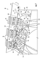
- FIG. 4 illustrates an exemplary distributed antenna system housing assembly 81 (referred to as “assembly 81 ”) that may be employed to provide an HEE, such as the HEE 12 in FIGS. 1-3 .
- the assembly 81 is configured to be easily assembled in a factory or in the field by a technician. Further, the assembly 81 supports a number of features that allow interface cards to be easily inserted and aligned with respect to a midplane interface card 82 to ensure that proper connections are made with other components of the HEE 12 that form part of the distributed antenna system, such as the optical-fiber based distributed antenna system 10 in FIGS. 1-3 , for example.
- the assembly 81 includes an enclosure 83 .
- the enclosure 83 is comprised of a bottom plate 84 and side plates 85 A, 85 B.
- An internal cavity 86 is formed in the space formed inside the bottom plate 84 and the side plates 85 A, 85 B when assembled together for locating components of the HEE 12 , such as the components illustrated in FIG. 2 , for example.
- a top plate (not shown) could also be provided and secured to the side plates 85 A, 85 B, to protect the internal cavity 86 and protect components of the HEE 12 disposed therein.
- the enclosure 83 is configured to support optical interface cards (OICs) 90 illustrated in FIG. 5 .
- An OIC 90 contains electronics and related optical components to convert electrical signals to optical signals to be distributed over optical fiber and vice versa.
- OICs 90 A, 90 B are grouped together in pairs to form an optical interface module (OIM) 91 .
- an OIM 91 is comprised of two (2) OICs 90 A, 90 B in this embodiment that each support up to three (3) RAUs 14 , and thus the OIM 91 supports up to six (6) RAUs 14 in this embodiment.
- OIM optical interface module
- each OIC 90 A, 90 B is provided as an electronics board 92 A, 92 B (e.g., a printed circuit board (PCB)) with integrated circuits provided therein to provide electrical signal to optical signal conversions for communication downlinks and vice versa for communication uplinks.
- An OIM plate 93 is provided to assist in coupling a pair of OICs 90 A, 90 B together to form the OIM 91 .
- the pair of OICs 90 A, 90 B is secured to the OIM plate 93 to form the OIM 91 .
- the OIM plate 93 serves to support the OICs 90 A, 90 B and contribute to the alignment of the OICs 90 A, 90 B for proper insertion into and attachment to the enclosure 83 , which in turn assists in providing for a proper and aligned connection of the OICs 90 A, 90 B to the midplane interface card 82 , as shown in FIG. 4 .
- the OICs 90 A, 90 B are also secured together via standoff connectors 94 that contain alignment features to allow self-alignment between the OICs 90 A, 90 B when connected to the midplane interface card 82 , as illustrated in FIG. 4 .
- Connector adapters 96 are disposed in the OIM plate 93 and provide for optical connections of the electronics boards 92 A, 92 B of the OICs 90 A, 90 B.
- the connector adapters 96 are disposed through openings 98 in the OIM plate 93 to provide external access when the OIM 91 is installed in the enclosure 83 .
- RAUs 14 can be connected to the connector adapters 96 to establish connections to the OICs 90 A, 90 B via the optical fiber cables connected to the connector adapters 96 .
- These connector adapters 96 may be configured to receive any type of fiber optic connector, including but not limited to FC, LC, SC, ST, MTP, and MPO.
- the OIM 91 is secured to the enclosure 83 via spring-loaded connector screws 100 disposed in the OIM plate 93 to secure the OIM plate 93 , and thus the OIM 91 , in the enclosure 83 , as illustrated in FIG. 4 .
- fiber routing guides 102 can be provided in the OIM 91 to assist in routing optical fibers 104 from the connector adapters 96 that are configured to connect to optical fibers 104 connected to the RAUs 14 (see FIG. 2 ).
- the optical fibers 104 are connected to the electronic components of the OICs 90 A, 90 B to convert the received uplink optical signals from the RAUs 14 into electrical signals to be distributed via an RF connector 106 .
- FIG. 7 is a top perspective view of an OIC 90 disposed in the OIM 91 of FIG. 5 and illustrating optical devices that are mounted or positioned on an end of the electronics board 92 to transmit and/or receive optical signals interfaced with electrical signal components disposed in the electronics board 92 .
- the optical devices are transmit optical sub-assemblies (TOSAs) 110 and receive optical sub-assemblies (ROSAs) 112 .
- TOSAs 110 and ROSAs 112 are connected via optical fiber tethers 114 , 115 to the connector adapters 96 that extend through the OIM plate 93 to allow connections to be made thereto.
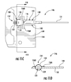
- FIGS. 8A and 8B illustrate an exemplary TOSA 110 .
- FIGS. 8A and 8B are perspective and side views, respectively, of the TOSA 110 with the optical fiber tether 114 connected to the TOSA 110 .
- the TOSA 110 is comprised of a body 116 that includes a can 118 .
- a fiber strain relief boot 120 is provided to provide strain relief between the optical fiber tether 114 and the body 116 .
- the can 118 contains a light source, such as a surface emitting laser diode matched to a lens in an end portion of the optical fiber tether 114 .
- electrical leads 122 are provided to electrically connect the laser in the can 118 .
- a flange 124 is disposed on the can 118 wherein the electrical leads 122 are disposed through the flange 124 .
- the electrical leads 122 must be connected to the desired electrical interface, such as through soldering or other connection type.
- the electrical leads 122 of the TOSA 110 are connected to an electrical connector or trace on the electronics board 92 .
- the TOSA 110 must also be mounted or disposed in some fashion with the electronics board 92 .
- the TOSAs 110 and ROSAs 112 are mounted or positioned on openings 126 , 128 , respectively, disposed on the electronics board 92 to transmit and/or receive optical signals interfaced with electrical signal components disposed in the electronics board 92 .
- Mounting or positioning of TOSAs 110 and ROSAs 112 in the openings 126 , 128 of the electronics board 92 has several features.
- the openings 126 , 128 allow the TOSAs 110 and ROSAs 112 to be disposed at an edge 130 of the electronics board 92 where the openings 126 , 128 start, but not at an end 132 of the electronics board 92 where the OIM plate 93 is located.
- the TOSAs 110 and ROSAs 112 are provided such that they do not interfere with or prevent the OIM plate 93 from being disposed at the end 132 of the electronics board 92 . It allows for the TOSAs 110 and ROSAs 112 to be edge mounted to the edge 130 of the electronics board 92 . This may limit the length of exposed, unshielded wire extensions between the TOSAs 110 and ROSAs 112 and printed traces on the electronics board 92 to minimize inductance in the wire extensions. This provides for preserved signal integrity of the signals after conversion to electrical signals.
- the openings 126 , 128 in the electronics board 92 in FIG. 7 in this embodiment are disposed completely in an interior portion 134 of the electronics board 92 .
- the openings 126 , 128 could be disposed in the electronics board 92 where a portion of the openings 126 , 128 are disposed at the end 132 of the electronics board 92 where the front sides 129 , 131 of openings 126 , 128 , respectively, disposed at the end 132 of the electronics board 92 .
- this configuration may be provided if there is room to locate the TOSAs 110 and ROSAs 112 to extend to the end 132 of the electronics board 92 .
- the TOSAs 110 and ROSAs 112 are edge mounted to the electronics board 92 to reduce the length between the electrical leads and the optical interface OIC interface board 92 to preserve signal integrity and to provide space for the TOSAs 110 and ROSAs 112 . Due to this edge mounting, it may also be important to mount the TOSAs 110 and ROSAs 112 in centered alignment in the openings 126 , 128 of the OIC electronics board 92 . Aligning the TOSAs 110 and ROSAs 112 to the openings 126 , 128 provides for proper electrical connection between the electrical leads 122 and the OIC electronics board 92 .
- a mis-alignment can cause a variation in impedance matching between the electrical leads 122 and the OIC electronics board 92 that can affect performance from designed performance characteristics. Further, it may be desired or required to provide additional grounding between the TOSAs 110 and ROSAs 112 to a ground node of the circuit provided in the OIC electronics board 92 to improve RF shielding of the TOSAs 110 and ROSAs 112 to reduce S/N ratios and preserve or improve performance as a result.
- the grounding provided between a ground lead of the electrical leads 122 and the OIC electronics board 92 may not be sufficient to provide sufficient RF shielding.
- FIGS. 9-23F illustrates examples of mounting devices that can also assist with alignment of these optical devices to an electronics board and inside openings of the electronics board and provide grounding of the optical devices to the electronics board.
- FIG. 9 is a rear perspective view of a first exemplary optical sub-assembly 140 that can be provided for mounting an optical device 142 to an electronics board 144 to provide an optical interface apparatus 146 .
- the optical device 142 mounted to the electronics board 144 is the TOSA 110 in FIGS. 8A and 8B .
- the optical interface apparatus 146 may be an optical interface card, such as the OIC 90 previously described above with regard to FIGS. 5-7 . Note that although a TOSA 110 is illustrated in FIG. 9 as being mounted to the electronics board 144 , the ROSA 112 or other optical device could also be mounted to the electronics board 144 in the same or similar fashion.
- the TOSA 110 of the optical sub-assembly 140 is disposed inside a board opening 148 in the electronics board 144 to edge mount the optical device 142 to the electronics board 144 , as previously discussed.
- the board opening 148 extends to an end 149 of the electronics board 144 .
- the board opening 148 does not have to extend to the end 149 of the electronics board 144 , such as is the case with the OIC 90 in FIGS. 5-7 .
- the board opening 148 forms a first opening edge 150 in the electronics board 144 .
- An optical interface 152 is disposed in the electronics board 144 adjacent to the first opening edge 150 .
- the electrical leads 122 of the TOSA 110 are connected to the optical interface 152 to electrically connect the TOSA 110 to the electrical circuit(s) in the electronics board 144 to provide the optical interface apparatus 146 .
- the optical signals generated by the TOSA 110 as a result of interfacing the TOSA 110 to the electronics board 144 are provided over the optical fiber tether 114 .
- FIGS. 10A-10D illustrate more detail of the mounting device 154 and its features and will be described below in more detail.
- the mounting device 154 contains features that allow the TOSA 110 to be edge mounted to the electronics board 144 in the board opening 148 such that the electrical leads 122 of the TOSA 110 can be electrically connected to the optical interface 152 adjacent the first opening edge 150 of the electronics board 144 .
- FIGS. 11A and 11B are front perspective and bottom perspective views, respectively, of the optical sub-assembly 140 mounted to electronics board 144 in FIG. 9 .
- FIGS. 11C and 11D are left top and rear side cross-sectional views, respectively, of the optical sub-assembly 140 mounted to the electronics board 144 in FIG. 9 .
- FIGS. 11E and 11F are bottom and front side cross-sectional views, respectively, of the optical sub-assembly 140 mounted to the electronics board 144 in FIG. 9 .
- the mounting device 154 also contains additional features.
- the mounting device 154 includes features that assist in aligning the flange 124 and can 118 of the TOSA 110 to the board opening 148 and the optical interface 152 when the TOSA 110 is mounted to the electronics board 144 using the mounting device 154 .
- the mounting device 154 is also configured to provide electrical contact with the flange 124 and can 118 of the TOSA 110 when mounting the TOSA 110 to the electronics board 144 .
- additional grounding i.e., lower impedance
- Providing additional grounding beyond grounding provided through a ground lead among the electrical leads 122 and the optical interface 152 may improve RF shielding of the TOSA 110 . This may assist in reducing or preventing radiated RF signals from the TOSA 110 from interfering with the ROSAs 112 as an example, and thus causing noise to be imposed on the receive circuits in the electronics board 144 connected to ROSAs 112 .
- Providing additional grounding with a grounding clamp connected to a ground lead among the electrical leads 122 may be difficult or not possible without damaging the TOSA 110 and/or due to coating on the connection point between the electrical leads 122 and the optical interface 152 .
- FIG. 10A is a perspective view of the mounting device 154 of the optical sub-assembly 140 of FIG. 9 .
- FIG. 10B is front view of the mounting device 154 of the optical sub-assembly 140 of FIG. 9 .
- FIGS. 10C and 10D are top and right side views, respectively, of the mounting device 154 of the optical sub-assembly 140 of FIG. 9 .
- the mounting device 154 includes a retention structure 158 .
- the retention structure 158 comprises a retention opening 160 disposed along a longitudinal axis L 1 of the retention structure 158 .
- the retention opening 160 in this embodiment has a geometric shape that is complementary to the geometric shape of the flange 124 and/or the can 118 of the TOSA 110 .
- the retention opening 160 is cylindrical shaped to be complementary with the cylindrical shape of the flange 124 and/or the can 118 of the TOSA 110 .
- the flange 124 is the largest outer diameter component of the TOSA 110 , and is disposed inside the retention opening 160 .
- the retention opening 160 supports the flange 124 , and the can 118 , of the TOSA 110 to secure the TOSA 110 in the board opening 148 of the electronics board 144 .
- the retention opening 160 can precisely retain the flange 124 and the can 118 of the TOSA 110 to hold the TOSA 110 in precise alignment in the board opening 148 and to align the electrical leads 122 with the optical interface 152 of the electronics board 144 .
- an inner diameter ID 1 of the retention opening 160 may be the same or slightly smaller than the largest outer diameter of the body 116 , flange 124 , or can 118 of the TOSA 110 .
- a friction fit is provided between the retention structure 158 and the TOSA 110 , as illustrated in FIG. 9 and FIGS. 11A-11F .
- a protrusion member 161 may also be provided in the retention structure 158 and disposed in the retention opening 160 to provide a stop for the flange 124 and allow the retention structure 158 to flex about the body 116 , flange 124 , or can 118 of the TOSA 110 disposed in the retention opening 160 and when the mounting surfaces 156 A, 156 B are secured to the electronics board 144 , as illustrated in FIG. 9 and FIGS. 11A-11F .
- the protrusion member 161 can also assist in providing additional friction fit/clamping between the retention structure 158 and the flange 124 or can 118 of the TOSA 110 .
- the mounting device 154 also includes the mounting surfaces 156 A, 156 B.
- the mounting surfaces 156 A, 156 B may be mounting tabs or other structures that extend from sides 162 A, 162 B of the retention structure 158 to support mounting of the mounting device 154 to each side of the board opening 148 when the TOSA 110 is disposed in the board opening 148 , as illustrated in FIG. 9 and FIGS. 11A-11F .
- the mounting surfaces 156 A, 156 B are disposed along a plane P 1 that intersects with the retention opening 160 , as illustrated in FIGS. 10A and 10B .
- the retention opening 160 will be disposed inside the board opening 148 such that the flange 124 and the can 118 of the TOSA 110 supported in the retention opening 160 will be disposed both about and below the electronics board 144 .
- the mounting surfaces 156 A, 156 B each contain through holes 164 A, 164 B that are configured to receive fasteners or solder to secure the mounting surfaces 156 A, 156 B to the electronics board 144 , and in turn secure the TOSA 110 supported in the retention opening 160 to the electronics board 144 .
- the retention structure 158 and the mounting surfaces 156 A, 156 B may be constructed from electrically conductive material, such as copper, silver, brass, steel, and any spring tempered copper alloy such as phosphor bronze or beryllium copper, as non-limiting examples.
- electrically conductive material such as copper, silver, brass, steel, and any spring tempered copper alloy such as phosphor bronze or beryllium copper, as non-limiting examples.
- the mounting surfaces 156 A, 156 B may be soldered to grounding nodes on the electronics board 144 to provide this additional grounding between the electronics board 144 and the TOSA 110 , as illustrated in FIG. 9 and FIGS. 11A-11F . Additional or improved grounding can improve RF shielding of the TOSA 110 .
- a surface area between eighty-five percent (85%) and ninety-five percent (95%) of the outer surface of the flange 124 e.g., eighty-nine percent (89%) may be placed into contact with the retention structure 158 to provide additional grounding in this embodiment. The greater the amount of surface contact between the mounting device 154 and the TOSA 110 , the lower the impedance and enhanced grounding.
- the protrusion member 161 provided in the retention structure 158 and disposed in the retention opening 160 may also assist to provide additional electrical contact between the flange 124 and/or the can 118 of the TOSA 110 to provide electrical contact between the flange 124 and the can 118 of the TOSA 110 and the mounting surfaces 156 A, 156 B for additional or improved grounding.
- FIG. 12 is a rear perspective view of another exemplary optical sub-assembly 170 that can be provided for mounting an optical device 172 to the electronics board 144 to provide another optical interface apparatus 176 .
- the optical device 172 mounted to the electronics board 144 is also the TOSA 110 in FIGS. 8A and 8B .
- the optical interface apparatus 176 may be an optical interface card, such as the OIC 90 previously described above with regard to FIGS. 5-7 .
- a TOSA 110 is illustrated in FIG. 12 as being mounted to the electronics board 144 , a ROSA 112 or other optical device could also be mounted to the electronics board 144 in the same or similar fashion.
- the TOSA 110 of the optical sub-assembly 170 is disposed inside the board opening 148 in the electronics board 144 to edge mount the optical device 172 to the electronics board 144 , as previously discussed.
- the board opening 148 extends to the end 149 of the electronics board 144 .
- the board opening 148 does not have to extend to the end 149 of the electronics board 144 , such as is the case with the OIC 90 in FIGS. 5-7 .
- the board opening 148 forms the first opening edge 150 in the electronics board 144 .
- the optical interface 152 is disposed in the electronics board 144 adjacent to the first opening edge 150 .
- the electrical leads 122 of the TOSA 110 are connected to the optical interface 152 to electrically connect the TOSA 110 to the electrical circuit(s) in the electronics board 144 to provide the optical interface apparatus 176 .
- the optical signals generated by the TOSA 110 as a result of interfacing the TOSA 110 to the electronics board 144 are provided over the optical fiber tether 114 .
- FIGS. 13A-13D illustrate more detail of the mounting device 184 and its features and will be described below in more detail.
- the mounting device 154 contains features that allow the TOSA 110 to be edge mounted to the electronics board 144 in the board opening 148 such that the electrical leads 122 of the TOSA 110 can be electrically connected to the optical interface 152 adjacent the first opening edge 150 of the electronics board 144 .
- FIGS. 14A and 14B are front perspective and bottom perspective views, respectively, of the optical sub-assembly 170 mounted to the electronics board 144 in FIG. 12 .
- FIGS. 14C and 14D are left top and rear side cross-sectional views, respectively, of the optical sub-assembly 170 mounted to the electronics board 144 in FIG. 9 .
- FIGS. 14E and 14F are bottom and front side cross-sectional views, respectively, of the optical sub-assembly 170 mounted to the electronics board 144 in FIG. 12 .
- the mounting device 184 also contains additional features.
- the mounting device 184 includes features that assist in aligning the flange 124 and the can 118 of the TOSA 110 to the board opening 148 and the optical interface 152 when the TOSA 110 is mounted to the electronics board 144 using the mounting device 184 .
- the mounting device 184 is also configured to provide electrical contact with the can 118 of the TOSA 110 when mounting the TOSA 110 to the electronics board 144 .
- additional grounding i.e., lower impedance
- Providing additional grounding beyond grounding provided through a ground lead among the electrical leads 122 and the optical interface 152 may improve RF shielding of the TOSA 110 . This may assist in reducing or preventing radiated RF signals from the TOSA 110 from interfering with the ROSAs 112 as an example, and thus causing noise to be imposed on the receive circuits in the electronics board 144 connected to ROSAs 112 .
- Providing additional grounding with a grounding clamp connected to a ground lead among the electrical leads 122 may be difficult or not possible without damaging the TOSA 110 and/or due to coating on the connection point between the electrical leads 122 and the optical interface 152 .
- FIG. 13A is a perspective view of the mounting device 184 of the optical sub-assembly 170 of FIG. 12 .
- FIG. 13B is front view of the mounting device 184 of the optical sub-assembly 170 of FIG. 12 .
- FIGS. 13C and 13D are top and right side views, respectively, of the mounting device 184 of the optical sub-assembly 170 of FIG. 12 .
- the mounting device 184 includes a retention structure 188 .
- the retention structure 188 comprises a retention opening 190 disposed along a longitudinal axis L 2 of the retention structure 188 .
- the retention opening 190 in this embodiment has a geometric shape that is complementary to the geometric shape of the flange 124 and/or the can 118 of the TOSA 110 .
- the retention opening 190 is cylindrical shaped to be complementary with the cylindrical shape of the flange 124 and/or the can 118 of the TOSA 110 .
- the flange 124 is the largest outer diameter component of the TOSA 110 , and is disposed inside the retention opening 190 .
- FIG. 12 and illustrated in more detail with regard to FIGS.
- the retention opening 190 supports the flange 124 and the can 118 of the TOSA 110 to secure the TOSA 110 in the board opening 148 of the electronics board 144 .
- the retention opening 190 can precisely retain the flange 124 and the can 118 of the TOSA 110 to hold the TOSA 110 in precise alignment in the board opening 148 and to align the electrical leads 122 with the optical interface 152 of the electronics board 144 .
- an inner diameter ID 2 of the retention opening 190 may be the same or slightly smaller than the outer diameter of the flange 124 or can 118 of the TOSA 110 . In this manner, a friction fit is provided between the retention structure 188 and the TOSA 110 , as illustrated in FIG. 12 and FIGS. 14A-14F .
- Protrusion members 191 A, 191 B, 191 C may also be provided in the retention structure 188 and disposed in the retention opening 190 to allow the retention structure 188 to flex about the body 116 , flange 124 , or can 118 of the TOSA 110 disposed in the retention opening 190 and when the mounting surfaces 186 A, 186 B are secured to the electronics board 144 , as illustrated in FIG. 12 and FIGS. 14A-14F .
- the protrusion members 191 A, 191 B, 191 C can also assist in providing additional friction fit/clamping between the retention structure 188 and the body 116 , flange 124 , or can 118 of the TOSA 110 .
- the mounting device 184 also includes the mounting surfaces 186 A, 186 B.
- the mounting surfaces 186 A, 186 B may be mounting tabs or other structures that extend from sides 192 A, 192 B of the retention structure 188 to support mounting of the mounting device 154 to each side of the board opening 148 when the TOSA 110 is disposed in the board opening 148 , as illustrated in FIG. 12 and FIGS. 14A-14F .
- the mounting surfaces 186 A, 186 B are disposed along a plane P 2 that intersects with the retention opening 190 , as illustrated in FIGS. 13A and 13B .
- the retention opening 190 will be disposed inside the board opening 148 such that the flange 124 and the can 118 of the TOSA 110 supported in the retention opening 190 will be disposed both about and below the electronics board 144 .
- the mounting surfaces 186 A, 186 B each contain through holes 194 A, 194 B that are configured to receive fasteners or solder to secure the mounting surfaces 186 A, 186 B to the electronics board 144 , and in turn secure the TOSA 110 supported in the retention opening 190 to the electronics board 144 .
- the retention structure 188 and the mounting surfaces 186 A, 186 B may be constructed from electrically conductive material, such as copper, silver, brass, steel, and any spring tempered copper alloy such as phosphor bronze or beryllium copper, as non-limiting examples.
- electrically conductive material such as copper, silver, brass, steel, and any spring tempered copper alloy such as phosphor bronze or beryllium copper, as non-limiting examples.
- the mounting surfaces 186 A, 186 B may be soldered to grounding nodes on the electronics board 144 to provide this additional grounding between the electronics board 144 and the TOSA 110 , as illustrated in FIG. 12 and FIGS. 14A-14F . Additional or improved grounding can improve RF shielding of the TOSA 110 . For example, a between eighty percent (80%) and ninety percent (90%) (e.g., eighty-six percent (86%)) of the outer surface of the flange 124 may be placed into contact with the retention structure 188 to provide additional grounding in this embodiment. The greater the amount of surface contact between the mounting device 184 and the TOSA 110 , the lower the impedance and enhanced grounding.
- the protrusion members 191 A, 191 B, 191 C provided in the retention structure 188 and disposed in the retention opening 190 may also assist to provide electrical contact between the flange 124 and/or the can 118 of the TOSA 110 to provide electrical contact between the flange 124 and/or the can 118 of the TOSA 110 and the mounting surfaces 186 A, 186 B for additional or improved grounding.
- the retention structure 188 contains an additional clamp 198 .
- the clamp 198 further assists in securing the flange 124 and/or the can 118 of the TOSA 110 firmly and securely in the retention opening 190 .
- the clamp 198 is comprised of two extension members 200 A, 200 B that extend down from each side 202 A, 202 B of the retention structure 188 such that the extension members 200 A, 200 B are disposed in parallel planes to each other.
- Each extension member 200 A, 200 B contains openings 204 A, 204 B that are configured to receive a fastener 206 therethrough, as illustrated in FIGS. 14B , 14 D, and 14 F.
- the fastener 206 may be threaded.
- the fastener 206 forces the extension members 200 A, 200 B to be bent toward each other to decrease the inner diameter ID 2 of the retention opening 190 around the flange 124 and/or the can 118 of the TOSA 110 as a clamp.
- Providing the clamp 198 may further assist in securing and/or aligning to the TOSA 110 in the board opening 148 and the electrical leads 122 to the optical interface.
- a gap or slot 208 between the extension members 200 A, 200 B also allows the optical fiber tether 114 to be disposed therein to allow the mounting device 184 to be slipped over a TOSA 110 during assembly even if the electrical leads 122 of the TOSA 110 are already secured to the electronics board 144 . This may be particularly beneficial if the optical fiber tether 114 is already connectorized, as is illustrated in FIG. 7 , wherein the slot 208 of the mounting device 184 is slipped over the optical fiber tether 114 between the TOSA 110 and the connector.
- FIG. 15 is a rear perspective view of another exemplary optical sub-assembly 210 that can be provided for mounting an optical device 212 to the electronics board 144 to provide another optical interface apparatus 216 .
- the optical device 212 mounted to the electronics board 144 is also the TOSA 110 in FIGS. 8A and 8B .
- the optical interface apparatus 216 may be an optical interface card, such as the OIC 90 previously described above with regard to FIGS. 5-7 . Note that although a TOSA 110 is illustrated in FIG. 15 as being mounted to the electronics board 144 , a ROSA 112 or other optical device could also be mounted to the electronics board 144 in the same or similar fashion.
- the TOSA 110 of the optical sub-assembly 210 is disposed inside the board opening 148 in the electronics board 144 to edge mount the optical device 212 to the electronics board 144 , as previously discussed.
- the board opening 148 extends to the end 149 of the electronics board 144 .
- the board opening 148 does not have to extend to the end 149 of the electronics board 144 , such as is the case with the OIC 90 in FIGS. 5-7 .
- the board opening 148 forms the first opening edge 150 in the electronics board 144 .
- the optical interface 152 is disposed in the electronics board 144 adjacent to the first opening edge 150 .
- the electrical leads 122 of the TOSA 110 are connected to the optical interface 152 to electrically connect the TOSA 110 to the electrical circuit(s) in the electronics board 144 to provide the optical interface apparatus 216 .
- the optical signals generated by the TOSA 110 as a result of interfacing the TOSA 110 to the electronics board 144 are provided over the optical fiber tether 114 .
- FIGS. 16A-16E illustrate more detail of the mounting device 224 and its features and will be described below in more detail.
- the mounting device 224 contains features that allow the TOSA 110 to be edge mounted to the electronics board 144 in the board opening 148 such that the electrical leads 122 of the TOSA 110 can be electrically connected to the optical interface 152 adjacent the first opening edge 150 of the electronics board 144 .
- FIGS. 17A and 17B are front perspective and bottom perspective views, respectively, of the optical sub-assembly 210 mounted to the electronics board 144 in FIG. 15 .
- FIGS. 17C and 17D are left top and rear side cross-sectional views, respectively, of the optical sub-assembly 210 mounted to the electronics board 144 in FIG. 15 .
- FIGS. 17E and 17F are bottom and front side cross-sectional views, respectively, of the optical sub-assembly 210 mounted to the electronics board 144 in FIG. 15 .
- the mounting device 224 also contains additional features.
- the mounting device 224 includes features that assist in aligning the flange 124 and the can 118 of the TOSA 110 to the board opening 148 and the optical interface 152 when the TOSA 110 is mounted to the electronics board 144 using the mounting device 224 .
- the mounting device 224 is also configured to provide electrical contact with the flange 124 and the can 118 of the TOSA 110 when mounting the TOSA 110 to the electronics board 144 .
- additional grounding i.e., lower impedance
- Providing additional grounding beyond grounding provided through a ground lead among the electrical leads 122 and the optical interface 152 may improve RF shielding of the TOSA 110 . This may assist in reducing or preventing radiated RF signals from the TOSA 110 from interfering with the ROSAs 112 as an example, and thus causing noise to be imposed on the receive circuits in the electronics board 144 connected to ROSAs 112 .
- Providing additional grounding with a grounding clamp connected to a ground lead among the electrical leads 122 may be difficult or not possible without damaging the TOSA 110 and/or due to coating on the connection point between the electrical leads 122 and the optical interface 152 .
- FIG. 16A is a perspective view of the mounting device 224 of the optical sub-assembly 210 of FIG. 15 .
- FIGS. 16B and 16C are front and rear views, respectively, of the mounting device 224 of the optical sub-assembly 210 of FIG. 15 .
- FIGS. 16D and 16E are top and left side views, respectively, of the mounting device 224 of the optical sub-assembly 210 of FIG. 15 .
- the mounting device 224 includes a retention structure 228 .
- the retention structure 228 comprising a retention opening 230 disposed along a longitudinal axis L 3 of the retention structure 228 .
- the retention opening 230 in this embodiment has a geometric shape that is complementary to the geometric shape of the flange 124 and/or the can 118 of the TOSA 110 .
- the retention opening 230 is cylindrical shaped to be complementary with the cylindrical shape of the flange 124 and/or the can 118 of the TOSA 110 .
- the flange 124 is the largest outer diameter component of the TOSA 110 , and is disposed inside the retention opening 230 .
- the retention opening 230 supports the flange 124 and the can 118 of the TOSA 110 to secure the TOSA 110 in the board opening 148 of the electronics board 144 .
- the retention opening 230 can precisely retain the flange 124 and the can 118 of the TOSA 110 to hold the TOSA 110 in precise alignment in the board opening 148 and to align the electrical leads 122 with the optical interface 152 of the electronics board 144 .
- an inner diameter ID 3 of the retention opening 230 may be the same or slightly smaller than the outer diameter of the flange 124 , and/or the can 118 of the TOSA 110 .
- a friction fit is provided between the retention structure 228 and the TOSA 110 , as illustrated in FIG. 15 and FIGS. 17A-17F .
- FIGS. 16A-16E As also illustrated in FIGS.
- the retention structure 228 also contains a larger inner diameter ID 4 that is created as a result of a counter bore disposed in the retention structure 228 to create the retention opening 230 having the inner diameter ID 3 .
- additional space is provided between the inner diameter ID 3 and the inner diameter ID 4 in the retention opening 230 so that there is room for the body 116 of the TOSA 110 to be retained loosely in the retention opening 230 while the flange 124 and the can 118 of the TOSA 110 is tightly retained therein.
- the mounting device 224 also includes the mounting surfaces 226 A, 226 B.
- the mounting surfaces 226 A, 226 B may be mounting tabs or other structures that extend from sides 232 A, 232 B of the retention structure 228 to support mounting of the mounting device 224 to each side of the board opening 148 when the TOSA 110 is disposed in the board opening 148 , as illustrated in FIG. 15 and FIGS. 17A-17F .
- the mounting surfaces 226 A, 226 B are disposed along a plane P 3 that intersects with the retention opening 230 , as illustrated in FIGS. 16A and 16B . In this manner, the retention opening 230 will be disposed inside the board opening 148 such that the flange 124 and/or the can 118 of the TOSA 110 supported in the retention opening 230 will be disposed both about and below the electronics board 144 .
- the retention structure 228 and the mounting surfaces 226 A, 226 B may be constructed from electrically conductive material, such as copper, silver, brass, steel, and any spring tempered copper alloy such as phosphor bronze or beryllium copper, as non-limiting examples.
- electrically conductive material such as copper, silver, brass, steel, and any spring tempered copper alloy such as phosphor bronze or beryllium copper, as non-limiting examples.
- the mounting surfaces 226 A, 226 B may be soldered to grounding nodes on the electronics board 144 to provide this additional grounding between the electronics board 144 and the TOSA 110 , as illustrated in FIG. 15 and FIGS. 17A-17F . Additional or improved grounding can improve RF shielding of the TOSA 110 . For example, a surface area between seventy percent (70%) and ninety-five percent (95%) of the outer surface of the flange 124 may be placed into contact with the retention structure 228 to provide additional grounding in this embodiment. The greater the amount of surface contact between the mounting device 224 and the TOSA 110 , the lower the impedance and enhanced grounding.
- the retention structure 228 contains an additional clamp 238 .
- the clamp 238 further assists in securing the flange 124 and/or the can 118 of the TOSA 110 firmly and securely in the retention opening 230 .
- the clamp 238 is compromised of two extension members 240 A, 240 B that extend down from each side 242 A, 242 B of the retention structure 228 such that the extension members 240 A, 240 B are disposed in parallel planes to each other.
- Each extension member 240 A, 240 B contains openings 244 A, 244 B that are configured to receive a fastener 246 therethrough, as illustrated in FIGS. 17B , 17 D, and 17 F.
- the fastener 246 may be threaded.
- the fastener 246 forces the extension members 240 A, 240 B to be bent toward each other to decrease the inner diameter ID 3 of the retention opening 230 around the flange 124 and/or the can 118 of the TOSA 110 as a clamp.
- Providing the clamp 238 may further assist in securing and/or aligning to the TOSA 110 in the board opening 148 and the electrical leads 122 to the optical interface 152 .
- a slot 248 between the extension members 240 A, 240 B also allows the optical fiber tether 114 to be disposed therein to allow the mounting device 244 to be slipped over the TOSA 110 during assembly even if the electrical leads 122 of the TOSA 110 are already secured to the electronics board 144 . This may be particularly beneficial if the optical fiber tether 114 is already connectorized, as is illustrated in FIG. 7 , wherein the slot 248 of the mounting device 244 is slipped over the optical fiber tether 114 between the TOSA 110 and the connector.
- FIG. 18 is a rear perspective view of another exemplary optical sub-assembly 250 that can be provided for mounting an optical device 252 to the electronics board 144 to provide another optical interface apparatus 256 .
- the optical device 252 mounted to the electronics board 144 is also the TOSA 110 in FIGS. 8A and 8B .
- the optical interface apparatus 256 may be an optical interface card, such as the OIC 90 previously described above with regard to FIGS. 5-7 .
- the TOSA 110 of the optical sub-assembly 250 is disposed inside the board opening 148 in the electronics board 144 to edge mount the optical device 252 to the electronics board 144 , as previously discussed.
- the board opening 148 extends to the end 149 of the electronics board 144 .
- the board opening 148 does not have to extend to the end 149 of the electronics board 144 , such as is the case with the OIC 90 in FIGS. 5-7 .
- the board opening 148 forms the first opening edge 150 in the electronics board 144 .
- the optical interface 152 is disposed in the electronics board 144 adjacent to the first opening edge 150 .
- the electrical leads 122 of the TOSA 110 are connected to the optical interface 152 to electrically connect the TOSA 110 to the electrical circuit(s) in the electronics board 144 to provide the optical interface apparatus 256 .
- the optical signals generated by the TOSA 110 as a result of interfacing the TOSA 110 to the electronics board 144 are provided over the optical fiber tether 114 .
- FIGS. 19A-19E illustrate more detail of the mounting device 264 and its features and will be described below in more detail.
- the mounting device 264 contains features that allow the TOSA 110 to be edge mounted to the electronics board 144 in the board opening 148 such that the electrical leads 122 of the TOSA 110 can be electrically connected to the optical interface 152 adjacent the first opening edge 150 of the electronics board 144 .
- FIGS. 20A and 20B are front perspective and bottom perspective views, respectively, of the optical sub-assembly 250 mounted to the electronics board 144 in FIG. 18 .
- FIGS. 20C and 20D are left top and rear side cross-sectional views, respectively, of the optical sub-assembly 250 mounted to the electronics board 144 in FIG. 18 .
- FIGS. 20E and 20F are bottom and front side cross-sectional views, respectively, of the optical sub-assembly 250 mounted to the electronics board 144 in FIG. 18 .
- the mounting device 264 also contains additional features.
- the mounting device 264 includes features that assist in aligning the flange 124 and/or the can 118 of the TOSA 110 to the board opening 148 and the optical interface 152 when the TOSA 110 is mounted to the electronics board 144 using the mounting device 264 .
- the mounting device 264 is also configured to provide electrical contact with the flange 124 and/or the can 118 of the TOSA 110 when mounting the TOSA 110 to the electronics board 144 .
- additional grounding i.e., lower impedance
- Providing additional grounding beyond grounding provided through a ground lead among the electrical leads 122 and the optical interface 152 may improve RF shielding of the TOSA 110 . This may assist in reducing or preventing radiated RF signals from the TOSA 110 from interfering with the ROSAs 112 as an example, and thus causing noise to be imposed on the receive circuits in the electronics board 144 connected to ROSAs 112 .
- Providing additional grounding with a grounding clamp connected to a ground lead among the electrical leads 122 may be difficult or not possible without damaging the TOSA 110 and/or due to coating on the connection point between the electrical leads 122 and the optical interface 152 .
- FIG. 19A is a perspective view of the mounting device 264 of the optical sub-assembly 250 of FIG. 18 .
- FIGS. 19B and 19C are front and rear views, respectively, of the mounting device 264 of the optical sub-assembly 250 of FIG. 18 .
- FIGS. 19D and 19E are top and left side views, respectively, of the mounting device 264 of the optical sub-assembly 250 of FIG. 18 .
- the mounting device 264 includes a retention structure 268 .
- the retention structure 268 comprises a retention opening 270 disposed along a longitudinal axis L 5 of the retention structure 268 .
- the retention opening 270 in this embodiment has a geometric shape that is complementary to the geometric shape of the flange 124 and/or the can 118 of the TOSA 110 .
- the retention opening 270 is cylindrical shaped to be complementary with the cylindrical shape of the flange 124 and/or the can 118 of the TOSA 110 .
- the flange 124 is the largest outer diameter component of the TOSA 110 , and is disposed inside the retention opening 270 .
- the retention opening 270 supports the flange 124 and the can 118 of the TOSA 110 to secure the TOSA 110 in the board opening 148 of the electronics board 144 .
- the retention opening 270 can precisely retain the flange 124 and the can 118 of the TOSA 110 to hold the TOSA 110 in precise alignment in the board opening 148 and to align the electrical leads 122 with the optical interface 152 of the electronics board 144 .
- an inner diameter ID 5 of the retention opening 270 may be the same or slightly smaller than the outer diameter of the flange 124 or the can 118 of the TOSA 110 .
- a friction fit is provided between the retention structure 268 and the TOSA 110 , as illustrated in FIG. 18 and FIGS. 20A-20F .
- FIGS. 19A-19E As also illustrated in FIGS.
- the retention structure 268 also contains a larger inner diameter ID 6 that is created as a result of a counter bore disposed in the retention structure 268 to create the retention opening 270 having the inner diameter ID 5 .
- additional space is provide between the inner diameter ID 5 and the inner diameter ID 6 in the retention opening 270 so that there is room for the flange 124 of the TOSA 110 to be retained loosely in the retention opening 270 while the can 118 and the flange 124 of the TOSA 110 is tightly retained therein.
- the mounting device 264 also includes the mounting surfaces 266 A, 266 B.
- the mounting surfaces 266 A, 266 B may be mounting tabs or other structures that extend from sides 272 A, 272 B of the retention structure 268 to support mounting of the mounting device 264 to each side of the board opening 148 when the TOSA 110 is disposed in the board opening 148 , as illustrated in FIG. 18 and FIGS. 20A-20F .
- the mounting surfaces 266 A, 266 B are disposed along a plane P 5 that intersects with the retention opening 270 , as illustrated in FIGS. 19A and 19B .
- the retention opening 270 will be disposed inside the board opening 148 such that the flange 124 of the TOSA 110 supported in the retention opening 270 will be disposed both above and below the electronics board 144 .
- the mounting surfaces 266 A, 266 B each contain through holes 274 A, 274 B that are configured to receive fasteners or solder to secure the mounting surfaces 266 A, 266 B to the electronics board 144 , and in turn secure the TOSA 110 supported in the retention opening 270 to the electronics board 144 .
- the retention structure 268 and the mounting surfaces 266 A, 266 B may be constructed from electrically conductive material, such as copper, silver, brass, steel, and any spring tempered copper alloy such as phosphor bronze or beryllium copper, as non-limiting examples.
- electrically conductive material such as copper, silver, brass, steel, and any spring tempered copper alloy such as phosphor bronze or beryllium copper, as non-limiting examples.
- the mounting surfaces 266 A, 266 B may be soldered to grounding nodes on the electronics board 144 to provide this additional grounding between the electronics board 144 and the TOSA 110 , as illustrated in FIG. 18 and FIGS. 20A-20F . Additional or improved grounding can improve RF shielding of the TOSA 110 . For example, a surface area between seventy percent (70%) and ninety-five percent (95%) of the outer surface of the flange 124 may be placed into contact with the retention structure 268 to provide additional grounding in this embodiment. The greater the amount of surface contact between the mounting device 264 and the TOSA 110 , the lower the impedance and enhanced grounding.
- the retention structure 268 contains an additional clamp 278 .
- the clamp 278 further assists in securing the flange 124 or the can 118 of the TOSA 110 firmly and securely in the retention opening 270 .
- the clamp 278 is comprised of two extension members 280 A, 280 B that extend down from each side 282 A, 282 B of the retention structure 268 such that the extension members 280 A, 280 B are disposed in parallel planes to each other.
- Each extension member 280 A, 280 B contains openings 284 A, 284 B that are configured to receive a fastener 286 therethrough, as illustrated in FIGS. 20B , 20 D, and 20 F.
- the fastener 286 may be threaded.
- the fastener 286 forces the extension members 280 A, 280 B to be bent toward each other to decrease the inner diameter ID 5 of the retention opening 270 around the flange 124 and/or the can 118 of the TOSA 110 as a clamp.
- Providing the clamp 278 may further assist in securing and/or aligning to the TOSA 110 in the board opening 148 and the electrical leads 122 to the optical interface.
- a slot 288 between the extension members 280 A, 280 B also allows the optical fiber tether 114 to be disposed therein to allow the mounting device 264 to be slipped over the TOSA 110 during assembly even if the electrical leads 122 of the TOSA 110 are already secured to the electronics board 144 . This may be particularly beneficial if the optical fiber tether 114 is already connectorized, as is illustrated in FIG. 7 , wherein the slot 288 of the mounting device 264 is slipped over the optical fiber tether 114 between the TOSA 110 and the connector.
- FIGS. 21A-21D are front top perspective, front bottom perspective, left top, and rear side cross-sectional views, respectively, of the mounting device 264 in FIGS. 18-20F mounted orthogonally to the electronics board 144 to provide an alternative optical sub-assembly 300 to secure the optical device of FIGS. 8A and 8B to an electronics board.
- the optical sub-assembly 300 that can be provided for mounting an optical device 302 to the electronics board 144 to provide another optical interface apparatus 306 .
- the optical device 302 mounted to the electronics board 144 is also the TOSA 110 in FIGS. 8A and 8B .
- the optical interface apparatus 306 may be an optical interface card, such as the OIC 90 previously described above with regard to FIGS. 5-7 .
- a TOSA 110 is illustrated in FIGS. 21A-21D as being mounted to the electronics board 144 , a ROSA 112 or other optical device could also be mounted to the electronics board 144 in the same or similar fashion.
- an optical sub-assembly 300 is provided where the optical device 302 is disposed inside the board opening 148 in the electronics board 144 to orthogonally mount the optical device 302 to the electronics board 144 to provide the optical interface apparatus 306 .
- grounding nodes 308 are disposed on the bottom side of the electronics board 44 as illustrated in FIG. 21B to allow the mounting device 264 to electrically contact the grounding nodes 308 when assembled and retaining the TOSA 110 .
- the optical device 302 is the TOSA 110 .
- the optical sub-assembly 300 includes the mounting device 264 having the same features in FIGS. 18-20F discussed above. Thus, these features are noted in FIGS.
- the electrical leads 122 run up through the board opening 148 in the electronics board from the TOSA 110 and are bent at an approximate right angle to be connected to the optical interface 152 .
- the electrical leads 122 could also be connected to the optical interface 152 without being bent.
- fiber optic cables and/or “optical fibers” include all types of single mode and multi-mode light waveguides, including one or more optical fibers that may be upcoated, colored, buffered, ribbonized and/or have other organizing or protective structure in a cable such as one or more tubes, strength members, jackets or the like.
- the optical fibers disclosed herein can be single mode or multi-mode optical fibers.
- other types of suitable optical fibers include bend-insensitive optical fibers, or any other expedient of a medium for transmitting light signals.
- An example of a bend-insensitive, or bend resistant, optical fiber is ClearCurve® Multimode fiber commercially available from Corning Incorporated. Suitable fibers of this type are disclosed, for example, in U.S. Patent Application Publication Nos. 2008/0166094 and 2009/0169163, the disclosures of which are incorporated herein by reference in their entireties.
Landscapes
- Physics & Mathematics (AREA)
- General Physics & Mathematics (AREA)
- Optics & Photonics (AREA)
- Electromagnetism (AREA)
- Engineering & Computer Science (AREA)
- Microelectronics & Electronic Packaging (AREA)
- Optical Couplings Of Light Guides (AREA)
- Structures For Mounting Electric Components On Printed Circuit Boards (AREA)
- Semiconductor Lasers (AREA)
- Optical Communication System (AREA)
- Shielding Devices Or Components To Electric Or Magnetic Fields (AREA)
- Combinations Of Printed Boards (AREA)
Abstract
Description
Claims (19)
Priority Applications (1)
| Application Number | Priority Date | Filing Date | Title |
|---|---|---|---|
| US13/405,559 US8855456B2 (en) | 2011-02-28 | 2012-02-27 | Mounting devices for optical devices, and related sub-assemblies, apparatuses, and methods |
Applications Claiming Priority (2)
| Application Number | Priority Date | Filing Date | Title |
|---|---|---|---|
| US201161447535P | 2011-02-28 | 2011-02-28 | |
| US13/405,559 US8855456B2 (en) | 2011-02-28 | 2012-02-27 | Mounting devices for optical devices, and related sub-assemblies, apparatuses, and methods |
Publications (2)
| Publication Number | Publication Date |
|---|---|
| US20120219263A1 US20120219263A1 (en) | 2012-08-30 |
| US8855456B2 true US8855456B2 (en) | 2014-10-07 |
Family
ID=46046290
Family Applications (1)
| Application Number | Title | Priority Date | Filing Date |
|---|---|---|---|
| US13/405,559 Expired - Fee Related US8855456B2 (en) | 2011-02-28 | 2012-02-27 | Mounting devices for optical devices, and related sub-assemblies, apparatuses, and methods |
Country Status (5)
| Country | Link |
|---|---|
| US (1) | US8855456B2 (en) |
| EP (1) | EP2681600A1 (en) |
| JP (1) | JP2014509784A (en) |
| CN (1) | CN103415798B (en) |
| WO (1) | WO2012161814A1 (en) |
Cited By (1)
| Publication number | Priority date | Publication date | Assignee | Title |
|---|---|---|---|---|
| US20160097907A1 (en) * | 2014-10-01 | 2016-04-07 | Clearfield, Inc. | Optical fiber management |
Families Citing this family (35)
| Publication number | Priority date | Publication date | Assignee | Title |
|---|---|---|---|---|
| US8452148B2 (en) | 2008-08-29 | 2013-05-28 | Corning Cable Systems Llc | Independently translatable modules and fiber optic equipment trays in fiber optic equipment |
| US11294136B2 (en) | 2008-08-29 | 2022-04-05 | Corning Optical Communications LLC | High density and bandwidth fiber optic apparatuses and related equipment and methods |
| US9075216B2 (en) | 2009-05-21 | 2015-07-07 | Corning Cable Systems Llc | Fiber optic housings configured to accommodate fiber optic modules/cassettes and fiber optic panels, and related components and methods |
| WO2010148336A1 (en) | 2009-06-19 | 2010-12-23 | Corning Cable Systems Llc | High density and bandwidth fiber optic apparatuses and related equipment and methods |
| US8593828B2 (en) * | 2010-02-04 | 2013-11-26 | Corning Cable Systems Llc | Communications equipment housings, assemblies, and related alignment features and methods |
| US8913866B2 (en) | 2010-03-26 | 2014-12-16 | Corning Cable Systems Llc | Movable adapter panel |
| AU2011265751B2 (en) | 2010-04-16 | 2015-09-10 | Corning Optical Communications LLC | Sealing and strain relief device for data cables |
| US8879881B2 (en) | 2010-04-30 | 2014-11-04 | Corning Cable Systems Llc | Rotatable routing guide and assembly |
| US9519118B2 (en) | 2010-04-30 | 2016-12-13 | Corning Optical Communications LLC | Removable fiber management sections for fiber optic housings, and related components and methods |
| US9075217B2 (en) | 2010-04-30 | 2015-07-07 | Corning Cable Systems Llc | Apparatuses and related components and methods for expanding capacity of fiber optic housings |
| US9279951B2 (en) | 2010-10-27 | 2016-03-08 | Corning Cable Systems Llc | Fiber optic module for limited space applications having a partially sealed module sub-assembly |
| US9116324B2 (en) | 2010-10-29 | 2015-08-25 | Corning Cable Systems Llc | Stacked fiber optic modules and fiber optic equipment configured to support stacked fiber optic modules |
| CA2819235C (en) | 2010-11-30 | 2018-01-16 | Corning Cable Systems Llc | Fiber device holder and strain relief device |
| WO2012106510A2 (en) | 2011-02-02 | 2012-08-09 | Corning Cable Systems Llc | Dense fiber optic connector assemblies and related connectors and cables suitable for establishing optical connections for optical backplanes in equipment racks |
| US9008485B2 (en) | 2011-05-09 | 2015-04-14 | Corning Cable Systems Llc | Attachment mechanisms employed to attach a rear housing section to a fiber optic housing, and related assemblies and methods |
| WO2013003303A1 (en) | 2011-06-30 | 2013-01-03 | Corning Cable Systems Llc | Fiber optic equipment assemblies employing non-u-width-sized housings and related methods |
| US8953924B2 (en) | 2011-09-02 | 2015-02-10 | Corning Cable Systems Llc | Removable strain relief brackets for securing fiber optic cables and/or optical fibers to fiber optic equipment, and related assemblies and methods |
| US9038832B2 (en) | 2011-11-30 | 2015-05-26 | Corning Cable Systems Llc | Adapter panel support assembly |
| US9250409B2 (en) | 2012-07-02 | 2016-02-02 | Corning Cable Systems Llc | Fiber-optic-module trays and drawers for fiber-optic equipment |
| US9042702B2 (en) | 2012-09-18 | 2015-05-26 | Corning Cable Systems Llc | Platforms and systems for fiber optic cable attachment |
| ES2551077T3 (en) | 2012-10-26 | 2015-11-16 | Ccs Technology, Inc. | Fiber optic management unit and fiber optic distribution device |
| US20140247541A1 (en) * | 2013-02-26 | 2014-09-04 | Realm Communications Group, Inc. | Telecom cabinet dual tray slider |
| US8985862B2 (en) | 2013-02-28 | 2015-03-24 | Corning Cable Systems Llc | High-density multi-fiber adapter housings |
| CN105870721B (en) * | 2015-01-20 | 2018-05-15 | 赛恩倍吉科技顾问(深圳)有限公司 | Interface fixing apparatus and circuit board assemblies |
| EP3465311B1 (en) * | 2016-06-06 | 2023-06-28 | Corning Optical Communications LLC | Telecommunications closure with point of connection plate holders |
| US11510329B2 (en) * | 2018-11-15 | 2022-11-22 | Hewlett Packard Enterprise Development Lp | Scalable-bandwidth aggregation for rack-scale servers |
| TWM617324U (en) * | 2019-10-31 | 2021-09-21 | 佑勝光電股份有限公司 | Optical transceiver module and an optical cable module |
| CA3195228A1 (en) | 2020-09-18 | 2022-03-24 | Nubis Communications Inc. | Data processing systems including optical communication modules |
| US11988874B2 (en) | 2020-10-07 | 2024-05-21 | Nubis Communications, Inc. | Data processing systems including optical communication modules |
| TW202238198A (en) | 2020-11-20 | 2022-10-01 | 美商紐比斯通訊股份有限公司 | Thermal design for rack mount systems including optical communication modules |
| US11698497B2 (en) * | 2021-03-04 | 2023-07-11 | Applied Optoelectronics, Inc. | Fiber holder for use with optical subassembly modules |
| US12461322B2 (en) * | 2021-06-17 | 2025-11-04 | Nubis Communications, Inc. | Communication systems having pluggable modules |
| US12405433B2 (en) | 2021-06-17 | 2025-09-02 | Nubis Communications, Inc. | Communication systems having pluggable modules |
| EP4152065A1 (en) | 2021-09-16 | 2023-03-22 | Nubis Communications, Inc. | Communication systems having co-packaged optical modules |
| US12489483B2 (en) * | 2022-08-10 | 2025-12-02 | Zebra Technologies Corporation | Wireless communications assemblies for mitigating radio frequency desensitization |
Citations (4)
| Publication number | Priority date | Publication date | Assignee | Title |
|---|---|---|---|---|
| US5127073A (en) | 1990-06-21 | 1992-06-30 | Amp Incorporated | Active device mount with push-pull optical fiber connector receptacle |
| US20030063397A1 (en) * | 2001-09-28 | 2003-04-03 | Sumitomo Electric Industries, Ltd. | Optical module |
| US6856769B1 (en) | 2000-10-24 | 2005-02-15 | Infineon Technologies Ag | Optical transceiver module |
| US20060045436A1 (en) | 2004-08-26 | 2006-03-02 | Wang Charlie X | Low electromagnetic interference (EMI) shielded assemblies for electro-optical devices |
Family Cites Families (6)
| Publication number | Priority date | Publication date | Assignee | Title |
|---|---|---|---|---|
| US7280724B2 (en) * | 2004-06-16 | 2007-10-09 | Sumitomo Electric Industries, Ltd. | Optical subassembly and optical transceiver installing the same |
| WO2006090847A1 (en) * | 2005-02-25 | 2006-08-31 | Fujitsu Limited | Optical transmitting/receiving apparatus |
| US7543993B2 (en) * | 2006-03-03 | 2009-06-09 | Hoya Corporation Usa | Fiber-coupled optical device mounted on a circuit board |
| JP4274222B2 (en) * | 2006-10-02 | 2009-06-03 | パナソニック電工株式会社 | Photoelectric conversion connector and manufacturing method thereof |
| US7787731B2 (en) | 2007-01-08 | 2010-08-31 | Corning Incorporated | Bend resistant multimode optical fiber |
| US20090169163A1 (en) | 2007-12-13 | 2009-07-02 | Abbott Iii John Steele | Bend Resistant Multimode Optical Fiber |
-
2012
- 2012-02-27 WO PCT/US2012/026705 patent/WO2012161814A1/en not_active Ceased
- 2012-02-27 US US13/405,559 patent/US8855456B2/en not_active Expired - Fee Related
- 2012-02-27 CN CN201280011892.4A patent/CN103415798B/en not_active Expired - Fee Related
- 2012-02-27 JP JP2013556758A patent/JP2014509784A/en active Pending
- 2012-02-27 EP EP12719818.2A patent/EP2681600A1/en not_active Withdrawn
Patent Citations (4)
| Publication number | Priority date | Publication date | Assignee | Title |
|---|---|---|---|---|
| US5127073A (en) | 1990-06-21 | 1992-06-30 | Amp Incorporated | Active device mount with push-pull optical fiber connector receptacle |
| US6856769B1 (en) | 2000-10-24 | 2005-02-15 | Infineon Technologies Ag | Optical transceiver module |
| US20030063397A1 (en) * | 2001-09-28 | 2003-04-03 | Sumitomo Electric Industries, Ltd. | Optical module |
| US20060045436A1 (en) | 2004-08-26 | 2006-03-02 | Wang Charlie X | Low electromagnetic interference (EMI) shielded assemblies for electro-optical devices |
Non-Patent Citations (1)
| Title |
|---|
| Patent Cooperation Treaty, International Preliminary Report on Patentability for PCT/US2012/026705, Sep. 3, 2013, 5 pages. |
Cited By (3)
| Publication number | Priority date | Publication date | Assignee | Title |
|---|---|---|---|---|
| US20160097907A1 (en) * | 2014-10-01 | 2016-04-07 | Clearfield, Inc. | Optical fiber management |
| US10012814B2 (en) * | 2014-10-01 | 2018-07-03 | Clearfield, Inc. | Optical fiber management |
| US10444458B2 (en) * | 2014-10-01 | 2019-10-15 | Clearfield, Inc. | Optical fiber management |
Also Published As
| Publication number | Publication date |
|---|---|
| CN103415798B (en) | 2015-09-02 |
| WO2012161814A8 (en) | 2013-09-19 |
| WO2012161814A1 (en) | 2012-11-29 |
| JP2014509784A (en) | 2014-04-21 |
| CN103415798A (en) | 2013-11-27 |
| EP2681600A1 (en) | 2014-01-08 |
| US20120219263A1 (en) | 2012-08-30 |
Similar Documents
| Publication | Publication Date | Title |
|---|---|---|
| US8855456B2 (en) | Mounting devices for optical devices, and related sub-assemblies, apparatuses, and methods | |
| US8992099B2 (en) | Optical interface cards, assemblies, and related methods, suited for installation and use in antenna system equipment | |
| US11114852B2 (en) | Power distribution module(s) capable of hot connection and/or disconnection for wireless communication systems, and related power units, components, and methods | |
| US10652636B2 (en) | Distributed antenna system architectures | |
| US9270374B2 (en) | Providing digital data services in optical fiber-based distributed radio frequency (RF) communications systems, and related components and methods | |
| US20130089332A1 (en) | Optical fiber-based distributed communications components, systems, and methods employing wavelength division multiplexing (wdm) for enhanced upgradability | |
| EP2868011B1 (en) | A communication link | |
| WO2012064333A1 (en) | Providing digital data services using electrical power line(s) in optical fiber-based distributed radio frequency (rf) communications systems, and related components and methods | |
| US6661565B2 (en) | Packaging for optical transceiver module | |
| EP2577891A1 (en) | Optical fiber -based distributed communications system and method employing wavelength division multiplexing (wdm) for enhanced upgradability | |
| CN213903870U (en) | Optical network unit | |
| EP2354826B1 (en) | Communications equipment housings, assemblies, and related alignment features and methods | |
| US11715949B2 (en) | Power distribution module(s) capable of hot connection and/or disconnection for wireless communication systems, and related power units, components, and methods |
Legal Events
| Date | Code | Title | Description |
|---|---|---|---|
| AS | Assignment |
Owner name: CORNING CABLE SYSTEMS LLC, NORTH CAROLINA Free format text: ASSIGNMENT OF ASSIGNORS INTEREST;ASSIGNORS:BEAMON, HUBERT BLAIR;COX, TERRY DEAN;REEL/FRAME:027766/0950 Effective date: 20120220 |
|
| STCF | Information on status: patent grant |
Free format text: PATENTED CASE |
|
| AS | Assignment |
Owner name: CORNING OPTICAL COMMUNICATIONS LLC, NORTH CAROLINA Free format text: CHANGE OF NAME;ASSIGNOR:CORNING CABLE SYSTEMS LLC;REEL/FRAME:040126/0818 Effective date: 20140114 |
|
| AS | Assignment |
Owner name: CCS TECHNOLOGY, INC., DELAWARE Free format text: ASSIGNMENT OF ASSIGNORS INTEREST;ASSIGNOR:CORNING OPTICAL COMMUNICATIONS LLC;REEL/FRAME:040663/0047 Effective date: 20160419 |
|
| AS | Assignment |
Owner name: CORNING OPTICAL COMMUNICATIONS LLC, NORTH CAROLINA Free format text: MERGER;ASSIGNORS:CCS TECHNOLOGY, INC.;CORNING OPTICAL COMMUNICATIONS BRANDS, INC.;REEL/FRAME:043601/0427 Effective date: 20170630 |
|
| MAFP | Maintenance fee payment |
Free format text: PAYMENT OF MAINTENANCE FEE, 4TH YEAR, LARGE ENTITY (ORIGINAL EVENT CODE: M1551) Year of fee payment: 4 |
|
| FEPP | Fee payment procedure |
Free format text: MAINTENANCE FEE REMINDER MAILED (ORIGINAL EVENT CODE: REM.); ENTITY STATUS OF PATENT OWNER: LARGE ENTITY |
|
| LAPS | Lapse for failure to pay maintenance fees |
Free format text: PATENT EXPIRED FOR FAILURE TO PAY MAINTENANCE FEES (ORIGINAL EVENT CODE: EXP.); ENTITY STATUS OF PATENT OWNER: LARGE ENTITY |
|
| STCH | Information on status: patent discontinuation |
Free format text: PATENT EXPIRED DUE TO NONPAYMENT OF MAINTENANCE FEES UNDER 37 CFR 1.362 |
|
| FP | Lapsed due to failure to pay maintenance fee |
Effective date: 20221007 |