US8854514B1 - Pixel array having wide dynamic range and good color reproduction and resolution and image sensor using the pixel array - Google Patents
Pixel array having wide dynamic range and good color reproduction and resolution and image sensor using the pixel array Download PDFInfo
- Publication number
- US8854514B1 US8854514B1 US14/306,965 US201414306965A US8854514B1 US 8854514 B1 US8854514 B1 US 8854514B1 US 201414306965 A US201414306965 A US 201414306965A US 8854514 B1 US8854514 B1 US 8854514B1
- Authority
- US
- United States
- Prior art keywords
- filters
- filter
- type photodiodes
- type
- photodiodes
- Prior art date
- Legal status (The legal status is an assumption and is not a legal conclusion. Google has not performed a legal analysis and makes no representation as to the accuracy of the status listed.)
- Active
Links
Images


Classifications
-
- H01L27/14603—
-
- H—ELECTRICITY
- H10—SEMICONDUCTOR DEVICES; ELECTRIC SOLID-STATE DEVICES NOT OTHERWISE PROVIDED FOR
- H10F—INORGANIC SEMICONDUCTOR DEVICES SENSITIVE TO INFRARED RADIATION, LIGHT, ELECTROMAGNETIC RADIATION OF SHORTER WAVELENGTH OR CORPUSCULAR RADIATION
- H10F39/00—Integrated devices, or assemblies of multiple devices, comprising at least one element covered by group H10F30/00, e.g. radiation detectors comprising photodiode arrays
- H10F39/80—Constructional details of image sensors
- H10F39/802—Geometry or disposition of elements in pixels, e.g. address-lines or gate electrodes
-
- H—ELECTRICITY
- H04—ELECTRIC COMMUNICATION TECHNIQUE
- H04N—PICTORIAL COMMUNICATION, e.g. TELEVISION
- H04N25/00—Circuitry of solid-state image sensors [SSIS]; Control thereof
- H04N25/50—Control of the SSIS exposure
- H04N25/57—Control of the dynamic range
-
- H—ELECTRICITY
- H04—ELECTRIC COMMUNICATION TECHNIQUE
- H04N—PICTORIAL COMMUNICATION, e.g. TELEVISION
- H04N25/00—Circuitry of solid-state image sensors [SSIS]; Control thereof
- H04N25/10—Circuitry of solid-state image sensors [SSIS]; Control thereof for transforming different wavelengths into image signals
- H04N25/11—Arrangement of colour filter arrays [CFA]; Filter mosaics
- H04N25/13—Arrangement of colour filter arrays [CFA]; Filter mosaics characterised by the spectral characteristics of the filter elements
- H04N25/134—Arrangement of colour filter arrays [CFA]; Filter mosaics characterised by the spectral characteristics of the filter elements based on three different wavelength filter elements
-
- H—ELECTRICITY
- H10—SEMICONDUCTOR DEVICES; ELECTRIC SOLID-STATE DEVICES NOT OTHERWISE PROVIDED FOR
- H10F—INORGANIC SEMICONDUCTOR DEVICES SENSITIVE TO INFRARED RADIATION, LIGHT, ELECTROMAGNETIC RADIATION OF SHORTER WAVELENGTH OR CORPUSCULAR RADIATION
- H10F39/00—Integrated devices, or assemblies of multiple devices, comprising at least one element covered by group H10F30/00, e.g. radiation detectors comprising photodiode arrays
- H10F39/80—Constructional details of image sensors
- H10F39/805—Coatings
- H10F39/8053—Colour filters
-
- H—ELECTRICITY
- H04—ELECTRIC COMMUNICATION TECHNIQUE
- H04N—PICTORIAL COMMUNICATION, e.g. TELEVISION
- H04N2209/00—Details of colour television systems
- H04N2209/04—Picture signal generators
- H04N2209/041—Picture signal generators using solid-state devices
- H04N2209/042—Picture signal generators using solid-state devices having a single pick-up sensor
- H04N2209/045—Picture signal generators using solid-state devices having a single pick-up sensor using mosaic colour filter
-
- H—ELECTRICITY
- H04—ELECTRIC COMMUNICATION TECHNIQUE
- H04N—PICTORIAL COMMUNICATION, e.g. TELEVISION
- H04N2209/00—Details of colour television systems
- H04N2209/04—Picture signal generators
- H04N2209/041—Picture signal generators using solid-state devices
- H04N2209/042—Picture signal generators using solid-state devices having a single pick-up sensor
- H04N2209/047—Picture signal generators using solid-state devices having a single pick-up sensor using multispectral pick-up elements
Definitions
- the present invention relates to an image sensor pixel array, and more particularly, to a pixel array having a wide dynamic range and good color reproduction and resolution and an image sensor using the pixel array.
- the light intensities are classified into several regions according to exposure times and photographing is performed as follows. First, image frame data that is picked up with a short exposure time is stored in a memory.
- FIG. 9 illustrates an image sensor according to a fourth embodiment of the present invention.
- a section ⁇ circumflex over (6) ⁇ between the light intensity A and the light intensity B is an effective usage section when the pixel has a large area
- a section ⁇ circumflex over (7) ⁇ between the light intensity C and the light intensity D is an effective usage section ⁇ circumflex over (8) ⁇ when the pixel has a small area.
- a section is an effective usage section when the pixel having a large area and the pixel having a small area are simultaneously used.
- the pixel array simultaneously using the photodiode having a large area and the photodiode having a small area to increase a dynamic range is proposed.
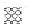
- FIG. 16 illustrates a portion of a pixel array according to the present invention.
- the pixel array include the photodiodes having the octagonal shape, the photodiodes having the square shape, and the image signal conversion circuits represented by the dotted lined circle.
Landscapes
- Engineering & Computer Science (AREA)
- Multimedia (AREA)
- Signal Processing (AREA)
- Physics & Mathematics (AREA)
- Spectroscopy & Molecular Physics (AREA)
- Solid State Image Pick-Up Elements (AREA)
- Color Television Image Signal Generators (AREA)
- Transforming Light Signals Into Electric Signals (AREA)
Abstract
Description
D({circumflex over (2)})=xA+yB
D({circumflex over (3)})=yA+xB [Equation 1]
Claims (3)
Priority Applications (1)
| Application Number | Priority Date | Filing Date | Title |
|---|---|---|---|
| US14/306,965 US8854514B1 (en) | 2007-06-18 | 2014-06-17 | Pixel array having wide dynamic range and good color reproduction and resolution and image sensor using the pixel array |
Applications Claiming Priority (6)
| Application Number | Priority Date | Filing Date | Title |
|---|---|---|---|
| KR1020070059575A KR100835894B1 (en) | 2007-06-18 | 2007-06-18 | Pixel array and image sensor with wide dynamic range and excellent color reproduction and resolution |
| KR10-2007-0059575 | 2007-06-18 | ||
| PCT/KR2007/005568 WO2008156232A1 (en) | 2007-06-18 | 2007-11-06 | Pixel array having wide dynamic range and good color reproduction and resolution and image sensor using the pixel array |
| US66354109A | 2009-12-08 | 2009-12-08 | |
| US13/875,773 US8792029B2 (en) | 2007-06-18 | 2013-05-02 | Pixel array having wide dynamic range and good color reproduction and resolution and image sensor using the pixel array |
| US14/306,965 US8854514B1 (en) | 2007-06-18 | 2014-06-17 | Pixel array having wide dynamic range and good color reproduction and resolution and image sensor using the pixel array |
Related Parent Applications (1)
| Application Number | Title | Priority Date | Filing Date |
|---|---|---|---|
| US13/875,773 Division US8792029B2 (en) | 2007-06-18 | 2013-05-02 | Pixel array having wide dynamic range and good color reproduction and resolution and image sensor using the pixel array |
Publications (2)
| Publication Number | Publication Date |
|---|---|
| US20140293099A1 US20140293099A1 (en) | 2014-10-02 |
| US8854514B1 true US8854514B1 (en) | 2014-10-07 |
Family
ID=39770329
Family Applications (3)
| Application Number | Title | Priority Date | Filing Date |
|---|---|---|---|
| US12/663,541 Abandoned US20100177221A1 (en) | 2007-06-18 | 2007-11-06 | Pixel array having wide dynamic range and good color reproduction and resolution and image sensor using the pixel array |
| US13/875,773 Active US8792029B2 (en) | 2007-06-18 | 2013-05-02 | Pixel array having wide dynamic range and good color reproduction and resolution and image sensor using the pixel array |
| US14/306,965 Active US8854514B1 (en) | 2007-06-18 | 2014-06-17 | Pixel array having wide dynamic range and good color reproduction and resolution and image sensor using the pixel array |
Family Applications Before (2)
| Application Number | Title | Priority Date | Filing Date |
|---|---|---|---|
| US12/663,541 Abandoned US20100177221A1 (en) | 2007-06-18 | 2007-11-06 | Pixel array having wide dynamic range and good color reproduction and resolution and image sensor using the pixel array |
| US13/875,773 Active US8792029B2 (en) | 2007-06-18 | 2013-05-02 | Pixel array having wide dynamic range and good color reproduction and resolution and image sensor using the pixel array |
Country Status (6)
| Country | Link |
|---|---|
| US (3) | US20100177221A1 (en) |
| EP (1) | EP2156659A4 (en) |
| JP (1) | JP2010531540A (en) |
| KR (1) | KR100835894B1 (en) |
| CN (1) | CN101682700B (en) |
| WO (1) | WO2008156232A1 (en) |
Cited By (2)
| Publication number | Priority date | Publication date | Assignee | Title |
|---|---|---|---|---|
| US11082625B2 (en) | 2019-01-18 | 2021-08-03 | Samsung Electronics Co., Ltd. | Imaging systems for generating HDR images and operating methods thereof |
| US20220137275A1 (en) * | 2020-11-02 | 2022-05-05 | Beijing Xiaomi Mobile Software Co., Ltd. | Color filter structure, related photographing method, device, terminal, and storage medium |
Families Citing this family (41)
| Publication number | Priority date | Publication date | Assignee | Title |
|---|---|---|---|---|
| US8237830B2 (en) | 2007-04-11 | 2012-08-07 | Red.Com, Inc. | Video camera |
| CN104702926B (en) | 2007-04-11 | 2017-05-17 | Red.Com 公司 | Video camera |
| US8717435B2 (en) * | 2008-04-09 | 2014-05-06 | Hbc Solutions, Inc. | Video monitoring device providing parametric signal curve display features and related methods |
| JP5574608B2 (en) * | 2009-03-10 | 2014-08-20 | キヤノン株式会社 | Color image sensor |
| KR101094246B1 (en) | 2009-03-16 | 2011-12-19 | 이재웅 | CMOS image sensor with wide dynamic range |
| JP2012015283A (en) * | 2010-06-30 | 2012-01-19 | Toshiba Corp | Solid-state imaging device manufacturing method |
| GB201011640D0 (en) * | 2010-07-12 | 2010-08-25 | Univ Sheffield | Radiation detection and method |
| KR101728713B1 (en) * | 2010-10-08 | 2017-04-21 | (주) 지안 | Wide Dynamic Range CMOS Image Sensor and Image Sensing Method |
| GB201102478D0 (en) | 2011-02-11 | 2011-03-30 | Isdi Ltd | Radiation detector and method |
| WO2013084406A1 (en) * | 2011-12-08 | 2013-06-13 | パナソニック株式会社 | Solid-state imaging device, and imaging device |
| KR101900914B1 (en) * | 2012-09-18 | 2018-11-05 | 삼성디스플레이 주식회사 | Organic light emitting display device |
| JP2016508700A (en) | 2013-02-14 | 2016-03-22 | レッド.コム,インコーポレイテッド | Video camera |
| US20140246561A1 (en) * | 2013-03-04 | 2014-09-04 | Omnivision Technologies, Inc. | High dynamic range pixel having a plurality of photodiodes with a single implant |
| US10225483B1 (en) * | 2013-05-01 | 2019-03-05 | Pierce Biotechnology, Inc. | Method and system for projecting image with differing exposure times |
| US10115034B2 (en) | 2013-05-01 | 2018-10-30 | Life Technologies Holdings Pte Limited | Method and system for projecting image with differing exposure times |
| JP2015065270A (en) * | 2013-09-25 | 2015-04-09 | ソニー株式会社 | Solid state image pickup device and manufacturing method of the same, and electronic apparatus |
| US9305949B2 (en) | 2013-11-01 | 2016-04-05 | Omnivision Technologies, Inc. | Big-small pixel scheme for image sensors |
| US20150146054A1 (en) * | 2013-11-27 | 2015-05-28 | Aptina Imaging Corporation | Image sensors with color filter elements of different sizes |
| US9324759B2 (en) | 2013-12-19 | 2016-04-26 | Omnivision Technologies, Inc. | Image sensor pixel for high dynamic range image sensor |
| CN103681721B (en) * | 2013-12-30 | 2018-10-16 | 上海集成电路研发中心有限公司 | Image sensor pixel array with high dynamic range |
| GB2525625B (en) | 2014-04-29 | 2017-05-31 | Isdi Ltd | Device and method |
| TWI625580B (en) | 2014-06-04 | 2018-06-01 | 元太科技工業股份有限公司 | Electrophoretic display device |
| JP2016054227A (en) | 2014-09-03 | 2016-04-14 | ソニー株式会社 | Solid-state image sensor, imaging apparatus and electronic apparatus |
| KR102261587B1 (en) | 2014-12-05 | 2021-06-04 | 삼성전자주식회사 | Image sensor for improving nonlinearty of low code region, method thereof, and device including the same |
| KR102210513B1 (en) | 2014-12-11 | 2021-02-02 | 삼성전자주식회사 | Image sensor for performing coupling-free readout, and device having the same |
| JP2017005111A (en) * | 2015-06-10 | 2017-01-05 | ソニー株式会社 | Solid state imaging device and electronic apparatus |
| KR102356706B1 (en) | 2015-07-07 | 2022-01-27 | 삼성전자주식회사 | Image Sensor Having Wide Dynamic Range, Pixel Circuit Of Image Sensor and Operating Method Thereof |
| US10879285B2 (en) * | 2015-09-11 | 2020-12-29 | Sony Semiconductor Solutions Corporation | Solid-state image pickup device to increase an area efficiency of a silicon interface on the transistor element side and electronic apparatus |
| US10148919B2 (en) * | 2015-10-15 | 2018-12-04 | Visera Technologies Company Limited | Image sensor having yellow filter units |
| US10110839B2 (en) | 2016-05-03 | 2018-10-23 | Semiconductor Components Industries, Llc | Dual-photodiode image pixel |
| US9843745B2 (en) | 2016-05-03 | 2017-12-12 | Semiconductor Components Industries, Llc | Image sensor pixels having separated charge storage regions |
| US10687003B2 (en) * | 2016-08-04 | 2020-06-16 | Omnivision Technologies, Inc. | Linear-logarithmic image sensor |
| US11019336B2 (en) | 2017-07-05 | 2021-05-25 | Red.Com, Llc | Video image data processing in electronic devices |
| US10312279B2 (en) | 2017-10-31 | 2019-06-04 | Semiconductor Components Industries, Llc | High dynamic range pixel with in-pixel light shield structures |
| CN108055485B (en) * | 2017-12-20 | 2020-08-25 | 思特威(上海)电子科技有限公司 | Imaging recovery method of multi-segment slope response image sensor |
| JP2019114728A (en) * | 2017-12-26 | 2019-07-11 | ソニーセミコンダクタソリューションズ株式会社 | Solid state imaging apparatus, distance measurement device, and manufacturing method |
| US10741592B2 (en) | 2018-06-07 | 2020-08-11 | Semiconductor Components Industries, Llc | Image sensors with multi-photodiode image pixels and vertical transfer gates |
| JP2020136429A (en) * | 2019-02-18 | 2020-08-31 | ソニーセミコンダクタソリューションズ株式会社 | Image sensor and image sensor |
| JP2023516410A (en) * | 2020-03-03 | 2023-04-19 | ホアウェイ・テクノロジーズ・カンパニー・リミテッド | Image sensor and image light sensing method |
| US12021105B2 (en) * | 2020-11-20 | 2024-06-25 | Taiwan Semiconductor Manufacturing Company, Ltd. | Pixel array including octagon pixel sensors |
| WO2023132137A1 (en) * | 2022-01-06 | 2023-07-13 | ソニーセミコンダクタソリューションズ株式会社 | Imaging element and electronic apparatus |
Citations (12)
| Publication number | Priority date | Publication date | Assignee | Title |
|---|---|---|---|---|
| JPH0378388A (en) * | 1989-08-22 | 1991-04-03 | Toshiba Corp | Color solid state image pickup element |
| JP2000125209A (en) * | 1998-10-12 | 2000-04-28 | Fuji Photo Film Co Ltd | Solid-state imaging device and signal reading method |
| JP2000125311A (en) * | 1998-10-12 | 2000-04-28 | Fuji Photo Film Co Ltd | Solid-state imaging device |
| JP2000350221A (en) * | 1999-06-04 | 2000-12-15 | Sanyo Electric Co Ltd | Digital camera and image pickup device |
| US20040046883A1 (en) * | 2002-09-09 | 2004-03-11 | Nobuo Suzuki | Solid-state image pick-up device |
| US20040096124A1 (en) * | 2002-11-15 | 2004-05-20 | Junichi Nakamura | Wide dynamic range pinned photodiode active pixel sensor (aps) |
| JP2004221265A (en) * | 2003-01-14 | 2004-08-05 | Fuji Photo Film Co Ltd | Solid-state image sensor and digital camera |
| JP2004228662A (en) * | 2003-01-20 | 2004-08-12 | Minolta Co Ltd | Imaging device |
| US20060119726A1 (en) * | 2004-11-19 | 2006-06-08 | Fuji Photo Film Co., Ltd. | Solid-state image sensor obviating degradation of image quality and apparatus using the same |
| JP2006190958A (en) * | 2004-12-10 | 2006-07-20 | Sony Corp | Physical information acquisition method and physical information acquisition device |
| JP2006270356A (en) * | 2005-03-23 | 2006-10-05 | Fuji Photo Film Co Ltd | Solid-state imaging device and solid-state imaging device |
| JP2006270364A (en) * | 2005-03-23 | 2006-10-05 | Fuji Photo Film Co Ltd | Solid-state imaging device, solid-state imaging device, and driving method thereof |
Family Cites Families (12)
| Publication number | Priority date | Publication date | Assignee | Title |
|---|---|---|---|---|
| US6107655A (en) * | 1997-08-15 | 2000-08-22 | Eastman Kodak Company | Active pixel image sensor with shared amplifier read-out |
| KR100308884B1 (en) | 1998-12-22 | 2001-11-22 | 박종섭 | Analog-to-Digital Converter for CMOS Image Sensors |
| JP4721380B2 (en) * | 2000-04-14 | 2011-07-13 | キヤノン株式会社 | Solid-state imaging device and imaging system |
| JP4734779B2 (en) * | 2001-06-22 | 2011-07-27 | 株式会社ニコン | Solid-state imaging device |
| JP3801126B2 (en) * | 2002-09-25 | 2006-07-26 | ソニー株式会社 | Imaging apparatus, image output method of imaging apparatus, and computer program |
| JP2004336469A (en) * | 2003-05-08 | 2004-11-25 | Fuji Film Microdevices Co Ltd | Solid-state imaging device, imaging apparatus, and image processing method |
| US7026596B2 (en) * | 2003-10-30 | 2006-04-11 | Micron Technology, Inc. | High-low sensitivity pixel |
| JP4500574B2 (en) * | 2004-03-30 | 2010-07-14 | 富士フイルム株式会社 | Wide dynamic range color solid-state imaging device and digital camera equipped with the solid-state imaging device |
| JP4469732B2 (en) * | 2004-05-07 | 2010-05-26 | 富士フイルム株式会社 | Solid-state image sensor |
| KR100674925B1 (en) * | 2004-12-07 | 2007-01-26 | 삼성전자주식회사 | Honeycomb Active Pixel Sensor |
| KR100710208B1 (en) * | 2005-09-22 | 2007-04-20 | 동부일렉트로닉스 주식회사 | CMOS image sensor and its manufacturing method |
| US7768569B2 (en) * | 2006-08-17 | 2010-08-03 | Altasens, Inc. | High sensitivity color filter array |
-
2007
- 2007-06-18 KR KR1020070059575A patent/KR100835894B1/en active Active
- 2007-11-06 JP JP2010513090A patent/JP2010531540A/en active Pending
- 2007-11-06 EP EP07833876.1A patent/EP2156659A4/en not_active Withdrawn
- 2007-11-06 CN CN2007800534149A patent/CN101682700B/en active Active
- 2007-11-06 US US12/663,541 patent/US20100177221A1/en not_active Abandoned
- 2007-11-06 WO PCT/KR2007/005568 patent/WO2008156232A1/en not_active Ceased
-
2013
- 2013-05-02 US US13/875,773 patent/US8792029B2/en active Active
-
2014
- 2014-06-17 US US14/306,965 patent/US8854514B1/en active Active
Patent Citations (13)
| Publication number | Priority date | Publication date | Assignee | Title |
|---|---|---|---|---|
| JPH0378388A (en) * | 1989-08-22 | 1991-04-03 | Toshiba Corp | Color solid state image pickup element |
| JP2000125209A (en) * | 1998-10-12 | 2000-04-28 | Fuji Photo Film Co Ltd | Solid-state imaging device and signal reading method |
| JP2000125311A (en) * | 1998-10-12 | 2000-04-28 | Fuji Photo Film Co Ltd | Solid-state imaging device |
| JP2000350221A (en) * | 1999-06-04 | 2000-12-15 | Sanyo Electric Co Ltd | Digital camera and image pickup device |
| US20040046883A1 (en) * | 2002-09-09 | 2004-03-11 | Nobuo Suzuki | Solid-state image pick-up device |
| US7489352B2 (en) * | 2002-11-15 | 2009-02-10 | Micron Technology, Inc. | Wide dynamic range pinned photodiode active pixel sensor (APS) |
| US20040096124A1 (en) * | 2002-11-15 | 2004-05-20 | Junichi Nakamura | Wide dynamic range pinned photodiode active pixel sensor (aps) |
| JP2004221265A (en) * | 2003-01-14 | 2004-08-05 | Fuji Photo Film Co Ltd | Solid-state image sensor and digital camera |
| JP2004228662A (en) * | 2003-01-20 | 2004-08-12 | Minolta Co Ltd | Imaging device |
| US20060119726A1 (en) * | 2004-11-19 | 2006-06-08 | Fuji Photo Film Co., Ltd. | Solid-state image sensor obviating degradation of image quality and apparatus using the same |
| JP2006190958A (en) * | 2004-12-10 | 2006-07-20 | Sony Corp | Physical information acquisition method and physical information acquisition device |
| JP2006270356A (en) * | 2005-03-23 | 2006-10-05 | Fuji Photo Film Co Ltd | Solid-state imaging device and solid-state imaging device |
| JP2006270364A (en) * | 2005-03-23 | 2006-10-05 | Fuji Photo Film Co Ltd | Solid-state imaging device, solid-state imaging device, and driving method thereof |
Cited By (4)
| Publication number | Priority date | Publication date | Assignee | Title |
|---|---|---|---|---|
| US11082625B2 (en) | 2019-01-18 | 2021-08-03 | Samsung Electronics Co., Ltd. | Imaging systems for generating HDR images and operating methods thereof |
| US11622081B2 (en) | 2019-01-18 | 2023-04-04 | Samsung Electronics Co., Ltd. | Imaging systems for generating HDR images and operating methods thereof |
| US20220137275A1 (en) * | 2020-11-02 | 2022-05-05 | Beijing Xiaomi Mobile Software Co., Ltd. | Color filter structure, related photographing method, device, terminal, and storage medium |
| US12196990B2 (en) * | 2020-11-02 | 2025-01-14 | Beijing Xiaomi Mobile Software Co., Ltd. | Color filter structure, related photographing method, device, terminal, and storage medium |
Also Published As
| Publication number | Publication date |
|---|---|
| WO2008156232A1 (en) | 2008-12-24 |
| KR100835894B1 (en) | 2008-06-09 |
| US20130242147A1 (en) | 2013-09-19 |
| CN101682700B (en) | 2012-02-29 |
| EP2156659A4 (en) | 2013-10-30 |
| US20140293099A1 (en) | 2014-10-02 |
| US20100177221A1 (en) | 2010-07-15 |
| JP2010531540A (en) | 2010-09-24 |
| US8792029B2 (en) | 2014-07-29 |
| EP2156659A1 (en) | 2010-02-24 |
| CN101682700A (en) | 2010-03-24 |
Similar Documents
| Publication | Publication Date | Title |
|---|---|---|
| US8854514B1 (en) | Pixel array having wide dynamic range and good color reproduction and resolution and image sensor using the pixel array | |
| JP4578797B2 (en) | Imaging device | |
| US7745779B2 (en) | Color pixel arrays having common color filters for multiple adjacent pixels for use in CMOS imagers | |
| KR100818987B1 (en) | An image pickup device and an operation method of the image pickup device | |
| US7440019B2 (en) | Solid-state image pick-up device | |
| CN205647747U (en) | Image sensor and image sensor system | |
| US20080211945A1 (en) | Image sensor with extended dynamic range | |
| US6956273B2 (en) | Photoelectric conversion element and solid-state image sensing device, camera, and image input apparatus using the same | |
| JP2006237737A (en) | Color filter array and solid-state imaging device | |
| US12136636B2 (en) | Image sensor, camera assembly and mobile terminal | |
| JP2007184904A (en) | Pixel array, imaging sensor including the pixel array and digital camera including the imaging sensor | |
| KR20110115072A (en) | Imaging device | |
| JP2012049619A (en) | Solid state image sensor and imaging apparatus | |
| JP5702895B2 (en) | Color imaging device and imaging apparatus | |
| CN104012085B (en) | Color image sensor | |
| US20150109494A1 (en) | Color imaging element and imaging device | |
| US7164444B1 (en) | Vertical color filter detector group with highlight detector | |
| KR100837454B1 (en) | Solid-state image sensing device | |
| JPH1126737A (en) | Solid-state imaging device | |
| KR20160072508A (en) | Color filter array and image sensor having the same | |
| EP2784820A1 (en) | Solid state imaging device | |
| KR100967651B1 (en) | CMOS image sensor device and its formation method | |
| US20090206241A1 (en) | Image sensor | |
| KR100746462B1 (en) | Unit pixel for color filter array | |
| KR20240041714A (en) | Image acquisition apparatus and electronic apparatus including the same, and method of controling the image acquisition apparatus |
Legal Events
| Date | Code | Title | Description |
|---|---|---|---|
| AS | Assignment |
Owner name: SILICONFILE TECHNOLOGIES INC., KOREA, REPUBLIC OF Free format text: ASSIGNMENT OF ASSIGNORS INTEREST;ASSIGNOR:LEE, DO-YOUNG;REEL/FRAME:033121/0254 Effective date: 20130425 |
|
| STCF | Information on status: patent grant |
Free format text: PATENTED CASE |
|
| FEPP | Fee payment procedure |
Free format text: PAYOR NUMBER ASSIGNED (ORIGINAL EVENT CODE: ASPN); ENTITY STATUS OF PATENT OWNER: LARGE ENTITY |
|
| AS | Assignment |
Owner name: SK HYNIX INC., KOREA, REPUBLIC OF Free format text: ASSIGNMENT OF ASSIGNORS INTEREST;ASSIGNOR:SILICONFILE TECHNOLOGIES INC.;REEL/FRAME:041023/0058 Effective date: 20161222 |
|
| MAFP | Maintenance fee payment |
Free format text: PAYMENT OF MAINTENANCE FEE, 4TH YEAR, LARGE ENTITY (ORIGINAL EVENT CODE: M1551) Year of fee payment: 4 |
|
| MAFP | Maintenance fee payment |
Free format text: PAYMENT OF MAINTENANCE FEE, 8TH YEAR, LARGE ENTITY (ORIGINAL EVENT CODE: M1552); ENTITY STATUS OF PATENT OWNER: LARGE ENTITY Year of fee payment: 8 |
|
| MAFP | Maintenance fee payment |
Free format text: PAYMENT OF MAINTENANCE FEE, 12TH YEAR, LARGE ENTITY (ORIGINAL EVENT CODE: M1553); ENTITY STATUS OF PATENT OWNER: LARGE ENTITY Year of fee payment: 12 |