US8854403B2 - Image forming apparatus with a TFT backplane for xerography without a light source - Google Patents
Image forming apparatus with a TFT backplane for xerography without a light source Download PDFInfo
- Publication number
- US8854403B2 US8854403B2 US12/366,680 US36668009A US8854403B2 US 8854403 B2 US8854403 B2 US 8854403B2 US 36668009 A US36668009 A US 36668009A US 8854403 B2 US8854403 B2 US 8854403B2
- Authority
- US
- United States
- Prior art keywords
- tfts
- tft
- latent image
- charge acceptance
- acceptance layer
- Prior art date
- Legal status (The legal status is an assumption and is not a legal conclusion. Google has not performed a legal analysis and makes no representation as to the accuracy of the status listed.)
- Active, expires
Links
Images


Classifications
-
- B—PERFORMING OPERATIONS; TRANSPORTING
- B41—PRINTING; LINING MACHINES; TYPEWRITERS; STAMPS
- B41J—TYPEWRITERS; SELECTIVE PRINTING MECHANISMS, i.e. MECHANISMS PRINTING OTHERWISE THAN FROM A FORME; CORRECTION OF TYPOGRAPHICAL ERRORS
- B41J2/00—Typewriters or selective printing mechanisms characterised by the printing or marking process for which they are designed
- B41J2/385—Typewriters or selective printing mechanisms characterised by the printing or marking process for which they are designed characterised by selective supply of electric current or selective application of magnetism to a printing or impression-transfer material
- B41J2/39—Typewriters or selective printing mechanisms characterised by the printing or marking process for which they are designed characterised by selective supply of electric current or selective application of magnetism to a printing or impression-transfer material using multi-stylus heads
-
- G—PHYSICS
- G03—PHOTOGRAPHY; CINEMATOGRAPHY; ANALOGOUS TECHNIQUES USING WAVES OTHER THAN OPTICAL WAVES; ELECTROGRAPHY; HOLOGRAPHY
- G03G—ELECTROGRAPHY; ELECTROPHOTOGRAPHY; MAGNETOGRAPHY
- G03G15/00—Apparatus for electrographic processes using a charge pattern
- G03G15/22—Apparatus for electrographic processes using a charge pattern involving the combination of more than one step according to groups G03G13/02 - G03G13/20
- G03G15/32—Apparatus for electrographic processes using a charge pattern involving the combination of more than one step according to groups G03G13/02 - G03G13/20 in which the charge pattern is formed dotwise, e.g. by a thermal head
Definitions
- the subject application relates to latent image formation in xerographic systems. While the systems and methods described herein relate to image formation in xerographic systems, it will be appreciated that the described techniques may find application in other image formation systems, other xerographic applications, and/or other imaging methods.
- Classical latent image formation in xerography consists of the following steps: charging the surface of the imaging member (e.g., a photoreceptor) with corona to create background surface potential; photo-generating free charge carriers within the areas that need to be toned; and changing surface potential in these areas by transporting photo-generated charge towards the surface.
- the imaging member e.g., a photoreceptor
- Photoreceptor-based xerography Disadvantages of photoreceptor-based xerography include low charge mobility, sensitivity to light shock, and the need of an expensive light source such as a raster output scanner (ROS) (e.g., a laser) that occupies a considerable space in the system and adds greatly to its cost. Additionally, exposure to a laser beam is associated with various parasitic effects that cause image distortion and limit resolution (see, e.g., Journal of Imaging Sci. and Tech, vol. 40, p. 327, 1996)
- ROS raster output scanner
- U.S. Pat. No. 6,100,909 (Haas and Kubby) describes an apparatus for forming an imaging member comprising an array of high voltage thin-film transistors (TFT) and capacitors.
- TFT thin-film transistors
- HVPS high-voltage power supply
- CAD charged-area detection
- a method of forming a latent image on a photoreceptor comprises charging a charge-acceptance layer coupled to a thin-film transistor (TFT) array on the photoreceptor, and selectively discharging pixels of the charge-accepting surface by adjusting a voltage across TFTs coupled to the respective pixels.
- the method further comprises performing a discharged area development (DAD) technique on the TFT array surface to develop the latent image on a print medium.
- DAD discharged area development
- a system that facilitates forming a latent image on a photoreceptor comprises a thin-film transistor (TFT) array comprising a plurality of TFTs coupled to a ground plane, and a charge acceptance layer deposited over the TFT array. Each TFT corresponds to a pixel the charge acceptance layer. The charge acceptance layer is charged with negative ion.
- the TFTs have a gate-to-source voltage (Vgs) that is adjustable to discharge respective pixels coupled to the respective TFTs to form a latent image.
- Vgs gate-to-source voltage
- Yet another feature relates to a method of forming a latent image on a photoreceptor, without a light source, comprising using thin-film transistors with an adjustable gate-to-source voltage to control electronic discharge of ions from pixel regions on a charge acceptance layer, and developing a latent image formed by discharged pixel regions on the charge acceptance layer using a discharged area development (DAD) technique.
- DAD discharged area development
- FIG. 1 illustrates a latent image forming system that facilitates latent image formation on a surface of an imaging member using a TFT backplane comprising a plurality of TFTs, which are also coupled to a charge acceptance layer.
- FIG. 2 illustrates a cross-section view of a single pixel of a TFT backplane device, which includes a TFT and a ground plane, in accordance with various aspects described herein.
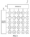
- FIG. 3 illustrates an array of pixel electrodes that uses an active matrix driving scheme in which a plurality of pixel electrodes are each connected to a switching device (TFT) as described herein.
- TFT switching device
- FIGS. 4 and 5 illustrate a latent image of surface charge using conventional row-by-row addressing of pixels to create the latent image of surface charge.
- FIG. 6 illustrates a method of latent image formation, in accordance with various aspects presented herein.
- systems and methods are described that facilitate using a TFT backplane with discharged area development (DAD) for latent image formation (e.g., whereby discharged area(s) on the imaging member surface correspond to an image on a print medium, and charged areas correspond to background).
- DAD discharged area development
- the described systems and methods facilitate forming latent images without the direct coupling of a high-voltage power source (HVPS) to the surface of the imaging member.
- HVPS high-voltage power source
- the current innovation proposes using corona charging to first create a background surface potential (Vbg) followed by selectively discharging individual pixels by using an array of TFTs to supply free charge carriers to reduce the electrostatic surface potential to nearly zero. This is followed by discharged area development to develop the latent image on a print medium (e.g., paper).
- a print medium e.g., paper.
- a latent image forming system 10 that facilitates latent image formation on a surface of an imaging member using a TFT backplane comprising a plurality of TFTs 14 , with the source electrodes connected to ground plane 12 and drain electrodes coupled to a charge acceptance layer 16 (e.g., a hole transport layer, insulator-conductive filler composite or the like).
- the system 10 uses TFT control for both electronic discharge for surface potential reduction and for latent image formation. Corona charging is employed to fully charge the charge acceptance layer 16 with charged particles 18 .
- the latent image formation via selective discharge of the surface is controlled by adjusting a voltage across one or more TFTs 14 .
- TFTs with a gate-to-source voltage (Vgs) of 0 will prevent discharging of the surface of the charge acceptance layer 16 .
- Other TFTs with a Vgs greater than a predetermined threshold voltage (Vth) for the TFT will enable a large surface charge by allowing charge of the opposite polarity to flow from the ground plane 12 to the opposite side of the charge acceptance layer 16 .
- Vgs gate-to-source voltage
- Vth threshold voltage
- the resolution of the latent image is limited only by the manufacturing capability of printed TFTs. For example, the image resolution may be 600 dpi or greater.
- the TFTs 14 may be organic or silicon-based, and a photosensitive device and a light source are not required for latent image generation.
- each TFT element corresponds to an individual pixel (e.g., an area or region of the charge acceptance layer 16 with a surface area equal to one image pixel).
- the charge acceptance layer 16 is charged using a corona device 20 .
- the corona device is a scorotron.
- a scorotron is a device that charges the charge acceptance layer 16 using one or more corona-producing wires. Between the corona-producing wires and the surface being e charged is a grid of wires. The corona emitting wires are maintained at a high voltage that maintains the wire grid at a desired surface-charging potential. Initially, the charge acceptance layer has a potential lower than desired, causing corona current to pass through the wire grid to the charge acceptance layer. When the charge acceptance layer potential and the wire grid potential are equal, corona current flow to the charge acceptance layer is terminated.
- Corona current is current that flows towards a corona wire when the wire is maintained at a high potential relative to ground (e.g., a corona threshold voltage, Vth).
- Ground e.g., a corona threshold voltage, Vth.
- Gas molecules e.g., air
- the ionized gas molecules flow away from the corona wire and form a positive current that is used to charge the charge acceptance layer 16 .
- Vth is the voltage at or above which a corona appears around the corona wire, due to gas molecule ionization.
- the charge acceptance layer 16 creates a background potential (Vbg) as well as a bias between the drain and source (ground) electrodes of the TFTs.
- Vbg background potential
- the proposed concept offers the following advantages over traditional photoreceptor xerography which are shown in Table 1: an exposure step and a need for a ROS are eliminated, therefore making the imaging process more reliable with less noise and fewer limiting factors for resolution; elimination of the ROS system allows for a more compact design; the imaging member is a digital device with a fixed resolution; the system 10 is stable to light shock; and long term cost advantage.
- Photoreceptor TFT imaging member Requires a light source Does not require a light source
- Analog device Digital device Resolution limited by Resolution is limited only dielectric thickness and by the planar integration depends on ROS density Light-sensitive Not light-sensitive, therefore easier handling Mobility 10 ⁇ 4 cm 2 /V * s Mobility 0.1-1.0 cm 2 /V * s
- the TFTs 14 have a 1:1 ratio with pixels electrodes 22 on the charge acceptance layer 16 (e.g., each pixel has a dedicated TFT to control whether it is charged or discharged). In another example, the TFTs have a ratio greater than 1:1 with the pixels 22 , for enhanced resolution.
- FIG. 2 illustrates a cross-section view of a single pixel of a TFT backplane 30 device, which includes a TFT 14 shown in FIG. 1 , in accordance with various aspects described herein.
- the TFT backplane 30 includes a TFT 14 that comprises semiconductor material 32 (e.g., organic or inorganic) and polymer-filler composite 34 that is coupled to a drain electrode 36 that serves as, or in conjunction with, a charge acceptance layer 16 for the imaging member.
- a source 38 is permanently connected to a ground electrode 12 (see FIG. 1 ).
- a voltage (Vgs) is applied to a gate electrode 40 by addressing it from the inner side of the device, supplying a current to reduce surface electrostatic potential to nearly zero.
- the gate electrode 40 is coupled to the data driver (see FIG. 3 ) and to a gate dielectric layer 42 , which in turn is coupled to the remainder of the TFT 14 (e.g., the drain 36 electrode, source or ground electrode 38 , and the semiconductor material 32 ).
- the drain 36 is electrostatically coupled to the surface of a scorotron (not shown) used to charge the charge acceptance layer of the imaging member on which the TFT backplane device 30 is employed, in order to supply charge thereto.
- a biased roll charging device (not shown) is used to charge the charge acceptance layer, such as is known by those of skill. Opening the transistor lets charge flow through the TFT to cancel charge from the scorotron, causing the expulsion of ions therefrom (e.g., discharge).
- the TFT backplane section shown in FIG. 2 is based on horizontal TFT. Additionally or alternatively, a vertical TFT design can be used. A guard electrode (not shown) may be introduced to prevent cross-talk between the TFT elements.
- substrate e.g., ground plane 16
- TFTs 14 amorphous silicon transistors are made by photolithography with a sputtered metal gate contact 40 followed by a silicon nitride gate dielectric 42 and an amorphous silicon channel, both deposited by plasma-enhanced chemical vapor deposition (CVD). This is followed by n-type doped amorphous silicon for the source contact 38 and drain contact 36 , and then a metal interconnect layer. A silicon oxynitride passivation may be formed layer over the top of the TFT.
- the source column electrodes are connected to a common ground and to gate electrodes connected to a gate driver.
- the drain electrodes 36 act as a high resolution switchable ground plane for the imaging member.
- a hole transport layer (not shown) is deposited.
- the hole transport layer may be similar or identical to the charge acceptance layer 16 of FIG. 1 .
- the hole transport layer comprises 50% N,N′-diphenyl-N,N-bis(3-methylphenyl)-1,1′-biphenyl-4,4′-diamine and 50% Makrolon and is 15% solids in CH 2 CL 2 .
- the layer is deposited using common solution web coating methods and dried in a forced air oven at, for example, 100° C. for 5 minutes.
- a scorotron device is then used to charge the surface of the device to a predetermined potential ( FIG. 4 ).
- selected TFTs under areas to be toned are switched “on” by applying Vgs>Vth to gate electrodes 38 , which causes the surface potential to drop to nearly zero in those selected areas. In this manner, a latent image is formed on the surface of the imaging member and is ready to be toned.
- the TFTs described herein operate at a threshold voltage (Vth) of approximately 40V.
- Vth threshold voltage
- TFTs are modified to withstand several hundred Volts (e.g., 200V-800V, in one example), while operating at 40V, by spacing the drain 36 and source 38 so that voltage is attenuated and the applied voltage is approximately 40V.
- FIG. 3 illustrates an array 50 of pixel electrodes 22 (also called a TFT array herein) that uses an active matrix driving scheme in which a plurality of pixel electrodes are each connected to a switching device (TFT) as described herein.
- An active substrate of an imaging device employing the array 50 contains a plurality of column (data) electrodes that are coupled to a data driver 54 (e.g., one or more integrated circuits or ICs), limited by the number of pixels 22 per row, and a plurality of row (scan) electrodes coupled to a scan driver 56 (e.g., one or more ICs), limited by the number of pixels per column.
- the scan electrodes control the gates of respective TFTs.
- Each switching TFT (coupled to the respective pixel electrodes) has a control (gate) terminal connected to the scan electrode, an input (source) terminal connected to the data electrode and an output (drain) terminal connected to a charge acceptance layer of the photoreceptor.
- two TFTs are provided per pixel, where a first TFT controls the gate of a second TFT to address a row of pixels (e.g., to hold the pixels open).
- a pattern on “ON” and/or “OFF” TFTs is written line by line.
- select voltages are applied to the gates of a first row of the TFTs while non-select voltages are applied to the TFT gates in all other pixel rows.
- Data voltages are applied at the same time to all of the column electrodes to discharge each pixel in the selected row to zero surface potential.
- the select voltage applied to the gates in the first row of TFTs is charged to a non-select voltage. This sequence is repeated for each succeeding row until all of the rows have been selected and the desired pixels have been discharged to form a latent image on the imaging device surface. After discharge area development, select voltages are applied to all row (gate) electrodes simultaneously to clear the latent image 72 .
- a dual scanning mode may be implemented.
- the array 50 is divided into two equal halves, and separate data and scan drivers are used for each of the two half-arrays.
- that half-array can be activated all at once to clear the partial latent image.
- the other half array can begin addressing its pixels to form the remainder of the latent image. This process can be repeated to obtain continuous mode printing.
- FIGS. 4 and 5 illustrate a latent image of surface charge using conventional row-by-row addressing of pixels to create the latent image of surface charge.
- an imaging member 70 having a layer of the TFT backplane described herein that is charged using a scorotron (not shown) or the like.
- a latent image 72 is formed on the imaging member by discharging areas corresponding to the latent image 72 . For instance, individual pixels are addressed row-by-row to form the latent image 72 , followed by discharge area development.
- FIG. 6 illustrates a method of latent image formation, in accordance with various aspects presented herein.
- a charge acceptance layer of a TFT array is charged using a corona device.
- the surface charge layer creates a background potential (Vbg) as well as a bias between the drain and source (ground) electrodes.
- areas to be toned e.g., to which toner is to adhere
- Vgs free charge carriers
- a discharge area development technique is performed to develop a physical image from the latent image.
- a production photoreceptor comprising a mylar substrate, a TiZr metalized layer on top of the substrate, and a N,N′-diphenyl-N,N-bis(3-methylphenyl)-1,1′-biphenyl-4,4′-diamine and 50% MakrolonTM charge transport layer (e.g., the charge acceptance layer 16 of FIG. 1 ) is overlaid on top of a photo-generating layer.
- the metalized TiZr backplane is switched between grounded and floating states. The device was then charged with, for instance, a 4200 Volt Scorotron, and surface charge may be measured with a capacitance probe.
- the charge acceptance layer shows a high level of charge acceptance when the backplane is floating.
- 90% discharge occurs.
- a TFT-switchable ground plane such as is described herein with regard to the various described embodiments, facilitates inducing selective electronic discharge of the surface potential, and latent image formation.
Landscapes
- Physics & Mathematics (AREA)
- General Physics & Mathematics (AREA)
- Printers Or Recording Devices Using Electromagnetic And Radiation Means (AREA)
Abstract
Description
| TABLE 1 |
| Advantages of the |
| photoreceptor-based technology |
| Photoreceptor | TFT imaging member | |
| Requires a light source | Does not require a light | |
| source | ||
| Analog device | Digital device | |
| Resolution limited by | Resolution is limited only | |
| dielectric thickness and | by the planar integration | |
| depends on ROS | density | |
| Light-sensitive | Not light-sensitive, | |
| therefore easier | ||
| handling | ||
| |
Mobility 0.1-1.0 cm2/V * s | |
Claims (12)
Priority Applications (1)
| Application Number | Priority Date | Filing Date | Title |
|---|---|---|---|
| US12/366,680 US8854403B2 (en) | 2009-02-06 | 2009-02-06 | Image forming apparatus with a TFT backplane for xerography without a light source |
Applications Claiming Priority (1)
| Application Number | Priority Date | Filing Date | Title |
|---|---|---|---|
| US12/366,680 US8854403B2 (en) | 2009-02-06 | 2009-02-06 | Image forming apparatus with a TFT backplane for xerography without a light source |
Publications (2)
| Publication Number | Publication Date |
|---|---|
| US20100201777A1 US20100201777A1 (en) | 2010-08-12 |
| US8854403B2 true US8854403B2 (en) | 2014-10-07 |
Family
ID=42540089
Family Applications (1)
| Application Number | Title | Priority Date | Filing Date |
|---|---|---|---|
| US12/366,680 Active 2031-04-08 US8854403B2 (en) | 2009-02-06 | 2009-02-06 | Image forming apparatus with a TFT backplane for xerography without a light source |
Country Status (1)
| Country | Link |
|---|---|
| US (1) | US8854403B2 (en) |
Families Citing this family (1)
| Publication number | Priority date | Publication date | Assignee | Title |
|---|---|---|---|---|
| US20250085648A1 (en) * | 2022-11-16 | 2025-03-13 | Beijing Boe Technology Development Co., Ltd. | Detection baseboard and control method thereof, detection device, and printing device |
Citations (5)
| Publication number | Priority date | Publication date | Assignee | Title |
|---|---|---|---|---|
| US5426488A (en) * | 1992-10-19 | 1995-06-20 | Sharp Kabushiki Kaisha | Method of charging a built-in electrophotographic charge member |
| US6100909A (en) | 1998-03-02 | 2000-08-08 | Xerox Corporation | Matrix addressable array for digital xerography |
| US6195196B1 (en) * | 1998-03-13 | 2001-02-27 | Fuji Photo Film Co., Ltd. | Array-type exposing device and flat type display incorporating light modulator and driving method thereof |
| US6780776B1 (en) * | 2001-12-20 | 2004-08-24 | Advanced Micro Devices, Inc. | Nitride offset spacer to minimize silicon recess by using poly reoxidation layer as etch stop layer |
| US20050259140A1 (en) * | 2004-05-19 | 2005-11-24 | Kim Seong-Jin | Electrostatic latent image forming medium, image forming apparatus including the electrostatic latent image forming medium and method of forming an electrostatic latent image |
-
2009
- 2009-02-06 US US12/366,680 patent/US8854403B2/en active Active
Patent Citations (5)
| Publication number | Priority date | Publication date | Assignee | Title |
|---|---|---|---|---|
| US5426488A (en) * | 1992-10-19 | 1995-06-20 | Sharp Kabushiki Kaisha | Method of charging a built-in electrophotographic charge member |
| US6100909A (en) | 1998-03-02 | 2000-08-08 | Xerox Corporation | Matrix addressable array for digital xerography |
| US6195196B1 (en) * | 1998-03-13 | 2001-02-27 | Fuji Photo Film Co., Ltd. | Array-type exposing device and flat type display incorporating light modulator and driving method thereof |
| US6780776B1 (en) * | 2001-12-20 | 2004-08-24 | Advanced Micro Devices, Inc. | Nitride offset spacer to minimize silicon recess by using poly reoxidation layer as etch stop layer |
| US20050259140A1 (en) * | 2004-05-19 | 2005-11-24 | Kim Seong-Jin | Electrostatic latent image forming medium, image forming apparatus including the electrostatic latent image forming medium and method of forming an electrostatic latent image |
Also Published As
| Publication number | Publication date |
|---|---|
| US20100201777A1 (en) | 2010-08-12 |
Similar Documents
| Publication | Publication Date | Title |
|---|---|---|
| US9167635B2 (en) | Light emitting apparatus, driving circuit of light emitting element, and driving method | |
| US6100909A (en) | Matrix addressable array for digital xerography | |
| US7948509B2 (en) | Line head and image forming device using the same | |
| US4794412A (en) | Vertical line width control ionographic system | |
| US5640189A (en) | Image forming apparatus using an electrode matrix to form a latent image | |
| US7388594B2 (en) | Electrostatic latent image forming medium, image forming apparatus including the electrostatic latent image forming medium and method of forming an electrostatic latent image | |
| US20160043345A1 (en) | Light-emitting device | |
| US8854403B2 (en) | Image forming apparatus with a TFT backplane for xerography without a light source | |
| US8643685B2 (en) | Photoreceptor with a TFT backplane for xerography without a ROS system | |
| US5581331A (en) | Color image forming apparatus | |
| KR100705427B1 (en) | Printer head and image forming apparatus having the same | |
| US20030123910A1 (en) | Image forming system in electrophotographic printer having an image charging unit and method for forming image using the same | |
| US10469693B2 (en) | Optical print head and image forming device | |
| US4719481A (en) | Electrographic ion writing head driver system | |
| JP4840304B2 (en) | Light emitting device and image forming apparatus having the same | |
| CN106886137A (en) | Optical writing device and image processing system | |
| US7995081B2 (en) | Anisotropically conductive backside addressable imaging belt for use with contact electrography | |
| JP6672937B2 (en) | Optical writing device and image forming device | |
| JP4640396B2 (en) | Exposure apparatus, exposure apparatus driving method, and image forming apparatus having the same | |
| US7411598B2 (en) | Line head and image forming apparatus | |
| Sheridon | Practical air-assisted ionographic printing | |
| US7071960B2 (en) | Image forming apparatus | |
| US20120069122A1 (en) | Electrostatic imaging member and methods for using the same | |
| JP2004106365A (en) | Image forming apparatus and copying apparatus | |
| JP6704719B2 (en) | Image forming device |
Legal Events
| Date | Code | Title | Description |
|---|---|---|---|
| AS | Assignment |
Owner name: XEROX CORPORATION, CONNECTICUT Free format text: ASSIGNMENT OF ASSIGNORS INTEREST;ASSIGNORS:SKOROKHOD, VLADISLAV;MCGUIRE, GREGORY;STREET, ROBERT A.;SIGNING DATES FROM 20090122 TO 20090126;REEL/FRAME:022216/0916 |
|
| FEPP | Fee payment procedure |
Free format text: PAYOR NUMBER ASSIGNED (ORIGINAL EVENT CODE: ASPN); ENTITY STATUS OF PATENT OWNER: LARGE ENTITY |
|
| STCF | Information on status: patent grant |
Free format text: PATENTED CASE |
|
| MAFP | Maintenance fee payment |
Free format text: PAYMENT OF MAINTENANCE FEE, 4TH YEAR, LARGE ENTITY (ORIGINAL EVENT CODE: M1551) Year of fee payment: 4 |
|
| MAFP | Maintenance fee payment |
Free format text: PAYMENT OF MAINTENANCE FEE, 8TH YEAR, LARGE ENTITY (ORIGINAL EVENT CODE: M1552); ENTITY STATUS OF PATENT OWNER: LARGE ENTITY Year of fee payment: 8 |
|
| AS | Assignment |
Owner name: CITIBANK, N.A., AS AGENT, DELAWARE Free format text: SECURITY INTEREST;ASSIGNOR:XEROX CORPORATION;REEL/FRAME:062740/0214 Effective date: 20221107 |
|
| AS | Assignment |
Owner name: XEROX CORPORATION, CONNECTICUT Free format text: RELEASE OF SECURITY INTEREST IN PATENTS AT R/F 062740/0214;ASSIGNOR:CITIBANK, N.A., AS AGENT;REEL/FRAME:063694/0122 Effective date: 20230517 |
|
| AS | Assignment |
Owner name: CITIBANK, N.A., AS COLLATERAL AGENT, NEW YORK Free format text: SECURITY INTEREST;ASSIGNOR:XEROX CORPORATION;REEL/FRAME:064760/0389 Effective date: 20230621 |
|
| AS | Assignment |
Owner name: JEFFERIES FINANCE LLC, AS COLLATERAL AGENT, NEW YORK Free format text: SECURITY INTEREST;ASSIGNOR:XEROX CORPORATION;REEL/FRAME:065628/0019 Effective date: 20231117 |
|
| AS | Assignment |
Owner name: XEROX CORPORATION, CONNECTICUT Free format text: TERMINATION AND RELEASE OF SECURITY INTEREST IN PATENTS RECORDED AT RF 064760/0389;ASSIGNOR:CITIBANK, N.A., AS COLLATERAL AGENT;REEL/FRAME:068261/0001 Effective date: 20240206 Owner name: CITIBANK, N.A., AS COLLATERAL AGENT, NEW YORK Free format text: SECURITY INTEREST;ASSIGNOR:XEROX CORPORATION;REEL/FRAME:066741/0001 Effective date: 20240206 |
|
| AS | Assignment |
Owner name: U.S. BANK TRUST COMPANY, NATIONAL ASSOCIATION, AS COLLATERAL AGENT, CONNECTICUT Free format text: FIRST LIEN NOTES PATENT SECURITY AGREEMENT;ASSIGNOR:XEROX CORPORATION;REEL/FRAME:070824/0001 Effective date: 20250411 |
|
| AS | Assignment |
Owner name: U.S. BANK TRUST COMPANY, NATIONAL ASSOCIATION, AS COLLATERAL AGENT, CONNECTICUT Free format text: SECOND LIEN NOTES PATENT SECURITY AGREEMENT;ASSIGNOR:XEROX CORPORATION;REEL/FRAME:071785/0550 Effective date: 20250701 |