US8853975B2 - Electrostatic actuator control - Google Patents
Electrostatic actuator control Download PDFInfo
- Publication number
- US8853975B2 US8853975B2 US13/247,919 US201113247919A US8853975B2 US 8853975 B2 US8853975 B2 US 8853975B2 US 201113247919 A US201113247919 A US 201113247919A US 8853975 B2 US8853975 B2 US 8853975B2
- Authority
- US
- United States
- Prior art keywords
- gaps
- actuator
- voltage
- cascaded
- gap
- Prior art date
- Legal status (The legal status is an assumption and is not a legal conclusion. Google has not performed a legal analysis and makes no representation as to the accuracy of the status listed.)
- Active, expires
Links
Images


Classifications
-
- H—ELECTRICITY
- H02—GENERATION; CONVERSION OR DISTRIBUTION OF ELECTRIC POWER
- H02N—ELECTRIC MACHINES NOT OTHERWISE PROVIDED FOR
- H02N1/00—Electrostatic generators or motors using a solid moving electrostatic charge carrier
-
- H—ELECTRICITY
- H02—GENERATION; CONVERSION OR DISTRIBUTION OF ELECTRIC POWER
- H02N—ELECTRIC MACHINES NOT OTHERWISE PROVIDED FOR
- H02N1/00—Electrostatic generators or motors using a solid moving electrostatic charge carrier
- H02N1/002—Electrostatic motors
- H02N1/006—Electrostatic motors of the gap-closing type
Definitions
- One or more embodiments relate generally to control of microelectromechanical systems (MEMS) and, more particularly, to control of MEMS electrostatic actuators.
- MEMS microelectromechanical systems
- a first type is denoted as gap-closing or parallel-plate MEMS actuators whereas a second type is denoted as an electrostatic comb actuator.
- a parallel-plate actuator includes two or more opposing plates. The plates are configured in the actuator such that a gap between them is closed as one plate is charged positively (or negatively) with respect to the opposing plate.
- Gap-closing actuators offer considerable actuation force as the electrostatic attraction between two opposite charges is inversely proportional to the square of the separation distance according to Coulomb's law. Thus as the gap separation is reduced towards zero, the electrostatic attractive force is markedly increased. Conversely, the electrostatic attractive force is markedly lowered as the gap separation is increased from zero.
- there is a relatively small range of travel for a conventional gap-closing actuator as the plates cannot be pulled too far apart from each other prior to actuation.
- an electrostatic comb actuator In contrast to gap-closing actuators, the separation between fingers in an electrostatic comb does not change. Rather than have the gap change, an electrostatic comb actuator varies the amount of overlap or interdigitation between the comb fingers. This interdigitation can occur over a relatively large range, depending upon the length of the comb fingers. Thus, comb actuators typically offer much better travel than gap-closing actuators. However, since the gap does not close, electrostatic combs are relatively weak in comparison to gap-closing actuators.
- gap-closing actuators that provide the travel advantages of a comb actuator.
- control of such improved gap-closing actuators is thus a need in the art for gap-closing actuators that provide the travel advantages of a comb actuator.
- MEMS actuators such as cascaded electrostatic actuators
- electrostatic actuators can be used to move lenses or to actuate shutters in cameras, for example.
- electrostatic actuators can be used in any desired application.
- a device in accordance with a first embodiment, includes: a cascaded electrostatic actuator defining a stack in a substrate having a plurality of gaps between parallel plate electrodes; and a controller configured to drive the cascaded electrostatic actuator to open and close selected ones of the gaps.
- a method of controlling a cascaded actuator includes: storing a plurality of first values corresponding to a plurality of gaps formed by a stack of parallel plates within a substrate; and driving a selected first one of the gaps with a voltage equaling the first value corresponding to the first one of the gaps to close the first one of the gaps.
- a method of controlling a cascaded actuator having a plurality of gaps formed by a stack of parallel plates within a substrate includes: driving the cascaded actuator with successive pulses of a first voltage to successively close the gaps.
- FIG. 1 shows a cellular telephone, in accordance with an embodiment.
- FIG. 2 is a block diagram of an actuator system, in accordance with an embodiment.
- FIG. 3 shows a cascaded electrostatic actuator, in accordance with an embodiment.
- FIG. 4 shows a cascaded electrostatic actuator in an unactuated state (with a voltage off), in accordance with an embodiment.
- FIG. 5 shows a cascaded electrostatic actuator in an actuated state (with a voltage on), in accordance with an embodiment.
- FIG. 6 shows a cascaded electrostatic actuator having two polysilicon hinges, in accordance with an embodiment.
- FIG. 7 shows a cascaded electrostatic actuator having one polysilicon hinge, in accordance with an embodiment.
- FIG. 8 shows a stack of a cascaded electrostatic actuator, in accordance with an embodiment.
- FIG. 9 shows an enlarged portion of the stack of FIG. 8 , in accordance with an embodiment.
- FIG. 10 shows a portion of the stack of FIG. 8 , in accordance with an embodiment.
- FIG. 11 shows an enlarged portion of the stack of FIG. 10 , in accordance with an embodiment.
- FIG. 12 shows a cascaded electrostatic actuator, in accordance with an embodiment.
- FIG. 13 shows a cascaded electrostatic actuator, in accordance with an embodiment.
- FIG. 14 shows a single cell of a cascaded electrostatic actuator in an unactuated state (with a voltage off), in accordance with an embodiment.
- FIG. 15 shows a single cell of a cascaded electrostatic actuator in an actuated state (with a voltage on), in accordance with an embodiment.
- FIG. 16 shows a plurality of staggered cells of a cascaded electrostatic actuator in an unactuated state (with a voltage off), in accordance with an embodiment.
- FIG. 17 shows a plurality of staggered cells of a cascaded electrostatic actuator in an actuated state (with a voltage on), in accordance with an embodiment.
- FIG. 18 shows a position versus voltage diagram for a first cascaded electrostatic actuator control method.
- FIG. 19 shows a position versus voltage diagram for a second cascaded electrostatic actuator control method.
- FIG. 20 a shows a voltage pulse waveform for controlling a cascaded electrostatic actuator.
- FIG. 20 b shows an actuator position responsive to the pulse waveform of FIG. 20 a.
- gap-closing actuators are stacked to provide what is denoted herein as a cascaded electrostatic actuator.
- Systems and methods are disclosed herein to provide control of microelectromechanical systems (MEMS) cascaded electrostatic actuators and applications therefor.
- a cascaded electrostatic actuator can comprise a plurality of alternating fingers, electrodes, plates, or layers upon which opposite charges can be placed so as to cause the alternating layers to move toward one another.
- Embodiments of the actuator can be controlled, for example, to move a shutter in a miniature camera to at least partially define an exposure and/or to move one or more lenses in a miniature camera to effect focus, zoom, or optical image stabilization (OIS).
- Embodiments of the actuator can be used to move or actuate various MEMS and non-MEMS devices.
- FIG. 1 shows a cellular telephone 100 , in accordance with an embodiment.
- the cellular telephone 100 can comprise a miniature camera 101 .
- the miniature camera 101 can comprise a cascaded electrostatic actuator 102 controlled to move at least one lens (such as lens 2801 of FIG. 28 ) of a lens assembly 103 .
- Such movement can effect focusing, zooming, and/or image stabilization, for example.
- FIG. 2 is a block diagram of a cascaded electrostatic actuator system, in accordance with an embodiment.
- the cascaded electrostatic actuator 102 can move a load 201 .
- the load 201 can be the lens 2801 of the lens assembly 103 for FIG. 1 , for example.
- the actuator 102 is controlled by a controller 203 .
- the controller 203 can be a microprocessor, such as a custom microprocessor or a general purpose microprocessor.
- the controller 203 can be dedicated to the operation of the actuator 102 or the controller 103 can also provide other functionality, such as functionally commonly associated with at least some portion of the operation of the cellular telephone 100 of FIG. 1 .
- a sensor 202 can sense the position, velocity, acceleration, and/or any other desired parameter associated with the load 201 .
- the sensor 202 can sense the position of the lens 2801 (see FIG. 28 ) of lens assembly 103 so as to facilitate focusing of the camera 101 , for example.
- the sensor 202 can provide an output representative of the sensed parameter to the controller 203 .
- the controller 203 can use the output of the sensor 202 to facilitate focusing of the camera 101 , for example, as discussed further herein.
- the controller 203 can control a display 204 .
- the display 204 can include any desired information.
- the display 204 can show the scene being photographed, can indicate whether an autofocus function is on or off and/or can indicate what portion of a scene being photographed is being used as the target for autofocusing.
- User controls 206 can affect operation of the actuator 102 , via the controller 203 .
- a user can operate the user controls 206 to zoom, turn autofocus on or off, and/or turn image stabilization on or off.
- a memory 205 can store programs for the controller 203 and/or can store other information.
- the memory 205 can store images captured by the camera 101 , parameters related to autofocus such as distance to the subject, and/or parameters for relating values sensed by the sensor 202 to positions of the lens 2801 (see FIG. 28 ).
- the cascaded electrostatic actuator control techniques disclosed herein may be applied to any stacked parallel-plate actuator.
- a particularly advantageous stacked architecture is disclosed in concurrently-filed U.S. application Ser. No. 13/247,847, entitled “Cascaded Electrostatic Actuator,” the contents of which are incorporated by reference.
- the parallel plates are defined in a semiconductor substrate.
- a series of parallel plates may be defined in a substrate with regard to a serpentine first electrode and a second electrode. Fingers in the second electrode interdigitate with folds in the serpentine first electrode to define the parallel plates in the plane of the semiconductor substrate.
- a first pair of parallel plates may defined by a first fold in the serpentine first electrode and a first finger for the second electrode.
- a second pair of parallel plates is defined by a second fold in the serpentine first electrode and a second finger for the second electrode, and so on. In this fashion, any number of parallel plate pairs may be defined by corresponding folds in the serpentine first electrode and fingers in the second electrode.
- cascaded architectures may be formed in the plane of the semiconductor substrate. For example a series of isolated plates may be formed through suitable etching of the substrate. Each isolated plate is surrounded by a circumferential gap that separates the plate from the surrounding substrate. The isolated plates and surrounding gaps form cells that may be stacked so that plates of substrate separate the cells. In this fashion, each isolated plate within the stack faces two opposing plates of substrate.
- Cascaded electrostatic actuator architectures are advantageous in that they are readily constructed using MEMS semiconductor manufacturing techniques as discussed further in the incorporated Cascaded Electrostatic Actuator application.
- a serpentine cascaded electrostatic actuator 103 includes a serpentine first electrode 301 .
- Each serpentine fold in electrode 301 corresponds to a pair of parallel plates in a series of such pairs.
- Each pair of parallel plates is formed by a fold in serpentine electrode 301 and a finger from a second electrode 302 .
- a first pair of parallel plates is defined by a first finger plate 315 for electrode 302 and a first fold plate 316 for electrode 302 .
- a second pair of parallel plates for actuator 103 corresponds to a second fold plate 326 and a second finger plate 320 .
- a third pair of parallel plates corresponds to a third finger plate 323 and a third fold plate 323 , and so on.
- each serpentine fold in electrode 301 corresponds to a pair of parallel plates in actuator 103 .
- Electrode 302 is separated from electrode 301 by a gap 303 .
- a single crystalline silicon substrate may be etched using conventional MEMS techniques to form what will become electrode 301 .
- the resulting trench surrounding electrode 301 may be partially filled with polysilicon to form electrode 302 as discussed further herein.
- electrode 301 may be polysilicon in that a serpentine trench may be etched that then partially filled with polysilicon.
- the surrounding silicon portion of the wafer will thus form fingers of electrode 302 that cooperate with folds in electrode 301 to form pairs of parallel plates.
- Electrode 302 forms opposing fingers that interdigitate with the serpentine folds of electrode 301 .
- finger 320 for electrode 302 opposes finger 315 .
- N the number of serpentine folds to define a stack 304
- N gaps 303 that may be collapsed during actuation.
- Stack 304 has an un-actuated (no voltage applied) height, Dimension L.
- Each gap 303 can have a un-actuated width, Dimension G. With N serpentine fold in stack 304 , there is thus a potential travel of N*G defining the range of motion for actuator 103 . In general, the travel of the actuator 102 can be approximately the width, Dimension G, of the gap 303 for a rest or un-actuated state for actuator 102 multiplied by the number of gaps 303 .
- a base 305 at one end of the stack 304 can define a proximal end 321 of the actuator 102 .
- the opposite end of the stack 304 can define a distal end 322 of the actuator 102 .
- the base 305 can be attached to one structure and the distal end 322 of the stack 304 can be attached to another structure such that actuation of the actuator effects relative movement of the two structures.
- the base 305 can be attached to a stationary portion (such as the lens barrel 2803 of FIG. 28 ) of the lens assembly 103 and the distal end 322 of the stack 304 can be attached to the lens 2801 (see FIG. 28 ) to effect movement of the lens 2801 for the focusing of the camera 101 .
- the base 305 can also facilitate electrical connection to the actuator 102 , as discussed herein.
- Electrical contract to the actuator 102 can be made in any desired manner.
- electrical contact can be made to a pad 311 formed of single crystalline silicon which can be in electrical communication with first electrode 301 and electrical contact can be made to the surrounding structure 312 formed of polysilicon which can be in electrical communication with the second electrode 302 .
- Actuation of the actuator 102 can result in sequential or simultaneous closure of the various gaps 303 due to the electrostatic force between the electrodes 301 and 302 .
- a gap closure is referred to as a snap-in motion.
- the distal end of the stack 304 moves quickly or snaps from its distal most or unactuated position to its proximal most or actuated position.
- substantially all the N gaps 303 corresponding to stack 304 move substantially simultaneously toward one another such that the stack 304 rapidly contracts in length, Dimension L.
- the stack 304 When unactuated, the stack 304 is expanded (has approximately the longest length, Dimension L, thereof). When actuated, the stack 304 is contracted (has approximately the shortest length, Dimension L, thereof).
- the different segments of the stack 304 can have different stiffness, such that the different segments of the stack 304 snap-in at different voltages.
- the voltage necessary for any given gap 303 to close is denoted as the pull-in voltage for that gap 303 and corresponding parallel plate pair.
- the pull-in voltage for that gap 303 and corresponding parallel plate pair is denoted as the pull-in voltage for that gap 303 and corresponding parallel plate pair.
- Different stiffnesses of the different segments of the stack 304 can be provided by fabricating the electrode 301 and/or the electrode 302 so as to have different widths within the different segments. Different stiffnesses of the different segments of the stack 304 can be provided by fabricating the electrode 301 and/or the electrode 302 so as to have different shapes within the different segments.
- Different widths, Dimension G, of the gap 303 can be used to provide different forces between given fingers of electrode 302 and corresponding surrounding serpentine folds of electrode 301 such that different gaps 303 snap in at different times (upon the application of different voltages). In this manner, smoother operation of the actuator 102 can be provided.
- the motion of the actuator 102 need not be snap-in, either as a whole or for segments thereof.
- the stiffness of the stack 304 can be substantially continuously non-linear such that the motion of the actuator 102 is substantially continuous.
- the distal end of the stack 304 can move generally continuously as the voltage applied to the actuator 102 is increased.
- the position or state of the actuator 102 (such as the position of the distal end 322 of the stack 304 ) can be determined by measuring the capacitance of the actuator 102 . That is, the capacitance between electrode 301 and electrode 302 can provide an indication of whether or not the actuator 102 is actuated and can provide an indication of the degree of actuation. The position of an portion of the actuator 102 can be determined by measuring the capacitance of that portion.
- the actuator 102 can be fabricated by etching a trench in a single crystalline substrate.
- the un-etched portions of the substrate can define electrode 301 .
- the trench can define electrode 301 .
- the trench can be filled with polysilicon to define electrode 302 or electrode 301 , depending upon which element the trench defines.
- An oxide layer can be formed to electrically isolate the electrodes during operation of the actuator 102 . The fabrication process is described in further detail herein.
- FIG. 4 shows the actuator 102 in an unactuated state (with a voltage off), in accordance with an embodiment.
- FIG. 5 shows the actuator 102 in an actuated state (with a voltage on), in accordance with an embodiment.
- electrodes 301 and 302 when no voltage is applied across electrodes 301 and 302 , then the charges on the electrodes are approximately the same. That is, electrodes 301 and 302 are at approximately the same electrical potential. Thus, there is no substantial force exerted between them. Since there is no substantial force exerted, the actuator 102 remains in an unactuated state.
- electrodes 301 and 302 when a voltage is applied across electrodes 301 and 302 , then the charges on the electrodes are substantially different with respect to one another. That is, electrodes 301 and 302 are at substantially different electrical potentials. Thus, there is a substantial attractive force exerted between electrodes 301 and 302 . Since there is a substantial force exerted, the actuator 102 moves or snaps in to an actuated state. In the actuated state, the stack 304 is compressed or contracted with respect to the unactuated state.
- An insulator such as an oxide layer 421 can be formed upon one or both of the electrodes 301 and 302 to inhibit shorting or electrical contact therebetween.
- the height, Dimension A, of the stack 304 of the unactuated actuator 102 of FIG. 4 is substantially greater than the height, Dimension B, of the stack 304 of the actuated actuator 102 of FIG. 5 .
- the distal end 322 of the stack 304 moves toward the base 305 of the actuator 102 .
- the amount of such movement can be approximately equal to the sum of the gaps 303 of the stack 304 .
- the amount of such movement can be greater than the width of a single gap 303 .
- An advantage of this cascaded configuration of the actuator 102 can be that more travel can be obtained by making the stack 304 thereof longer. That is, as more gaps 303 are added to stack 304 , the total amount of travel of the distal end 322 of the stack 304 obtained when the actuator 102 is actuated is proportionally increased.
- Another advantage of this cascaded configuration of the actuator 102 can be that more force can be provided.
- the electrostatic force provided by such an actuator is proportional to the cross-sectional area of the electrodes 301 and 302 .
- increased force can be obtained by making the thickness, Dimension T of FIG. 8 and/or the width, Dimension W of FIG. 8 , greater.
- Substantial forces can be provided by the cascaded configuration. For example, a 1 mm wide, 150 ⁇ m thick actuator 102 can produce approximately 10 grams of force.
- a first electrical contact 401 and a second electrical contact 402 can be formed from or upon the base 305 .
- the first electrical contact 401 can be formed from the material of the first electrode 301 , e.g., single crystalline silicon
- the second electrical contact 402 can be formed from the material of the electrode 302 , e.g., polysilicon.
- the first electrical contact 401 can be formed along with the first electrode 301 during the fabrication process and can thus be in electrical contact with electrode 301 .
- the second electrical contact 402 can be formed upon the base 305 after the first electrode and the second electrode have been fabricated, as discussed herein.
- the second electrical contact 402 can be electrically insulated from the base 305 , such as via an oxide layer (not shown) formed therebetween.
- the second electrical contact 402 can be in electrical contact with the second electrode 302 , such as where the second electrical contact 402 is formed thereover.
- Electrical connection can be made to the first electrical contact 401 and the second electrical contact 402 in the manner that electrical connection is commonly made to the pads or electrical contacts of integrated circuits.
- electrical connection can be made via wire bonding.
- FIG. 6 shows a cascaded electrostatic actuator 102 having a first polysilicon hinge 601 and a second polysilicon hinge 602 , in accordance with an embodiment.
- the first polysilicon hinge 601 and the second polysilicon hinge 602 cooperate to cause the distal end 322 of the stack 304 to flex or bend downwardly, out of the plane of the actuator 102 during actuation. In this manner, a more complex, non-linear motion can be obtained.
- the motion of the distal end of the stack 304 can depend, at least partially, upon the stiffness of the first polysilicon hinge 601 and the second polysilicon hinge 602 .
- the stiffness of the first polysilicon hinge 601 and the second polysilicon hinge 602 can depend upon the width and thickness (e.g., the cross-sectional area) thereof.
- the motion of the distal end of the stack 304 can have both translational (linear) and rotational (non-linear) components.
- the stiffer the first polysilicon hinge 601 and the second polysilicon hinge 602 the less the translational component will be and the greater the rotational component will be.
- the first polysilicon hinge 601 and the second polysilicon hinge 602 can have different stiffnesses, such that more complex motion of the distal end of the stack 304 can be provided.
- the first polysilicon hinge 601 and the second polysilicon hinge 602 inhibit or prevent the upper surface 603 of the stack 304 from contracting when the actuator 102 is actuated. As the lower surface of the actuator contracts, generally along the centerline or movement axis 611 , the distal end of the stack 304 curls down along an arc, approximately about an axis 612 .
- the distal end of the stack 304 can have a rotational component, and can have some linear component as well (depending upon the stiffness of the first polysilicon hinge 601 and the second polysilicon hinge 602 ). Such motion can be desirable in those instances where linear motion is inadequate.
- the use of an actuator that directly provides motion with such a rotational component has the advantage of not requiring additional structure to convert the motion from a linear actuator into a desired non-linear motion.
- FIG. 7 shows a cascaded electrostatic actuator having one polysilicon hinge, i.e., the first 601 polysilicon hinge, in accordance with an embodiment.
- the first polysilicon hinge 601 can cause the distal end of the stack 304 to flex or bend downwardly, out of the plane of the actuator 102 , and to twist at the same time. Such twisting can result in some lateral movement of the distal end of the stack 304 . In this manner, a more complex, non-linear motion can be obtained.
- the motion of the distal end of the stack 304 can depend, at least partially, upon the stiffness of the first polysilicon hinge 601 .
- the stiffness of the first polysilicon hinge 601 can depend upon the width and thickness (e.g., the cross-sectional area) thereof.
- the motion of the distal end of the stack 304 can have both translational (linear) and rotational (non-linear) components.
- the rotational components can be about two or more separate axes. Generally, the stiffer the first polysilicon hinge 601 , the less the translational component will be and the greater the rotational components will be.
- the use of only the first polysilicon hinge 601 adds stiffness to the stack 304 asymmetrically. Such asymmetric stiffness result in the more complex bending and twisting motion of the stack 304 during actuation and de-actuation.
- the first polysilicon hinge 601 can inhibit or prevent the one side (the left side as shown in FIG. 7 ) of the upper surface 603 of the stack 304 from contracting when the actuator 102 is actuated. As the lower surface and right side of the actuator contract generally along the centerline or movement axis 611 , the distal end of the stack 304 curls down along an arc, such as about axis 612 , and also twists, such as about a centerline or axis 611 .
- the distal end 322 of the stack 304 can have two rotational components (bending and twisting), and can have some linear component as well (depending upon the stiffness of the first polysilicon hinge 601 and/or the second polysilicon hinge 602 .
- Such motion can be desirable in those instances where linear motion is inadequate.
- the use of an actuator that directly provides motion with such a rotational component has the advantage of not requiring additional structure to convert the motion from a linear actuator into a desired non-linear motion.
- FIG. 8 shows the stack 304 (or a portion of the stack 304 ) in perspective, in accordance with an embodiment.
- the stack 304 can have a thickness, Dimension T; a width, Dimension W; and a length, Dimension L.
- the stack 304 is made up of the first electrode 301 and the second electrode 302 . Consequently, each of the electrodes have approximately the same thickness, Dimension T and approximately the same width, Dimension W.
- electrodes 301 and 302 have opposing faces of thickness T and width W.
- the area of these opposing surfaces determines the electrostatic force generated across gap 303 .
- the greater this area is, the greater the electrostatic force is across each gap 303 .
- FIG. 9 shows an enlarged portion of the stack 304 of FIG. 8 , in accordance with an embodiment.
- the serpentine fold plates for electrode 301 can have a thickness, Dimension D, which can be approximately 6 ⁇ m, for example.
- the finger plates formed by electrode 302 can have a thickness, Dimension E, which can be approximately 6 ⁇ m, for example.
- the thickness, Dimension D, of the serpentine structure for the first electrode can be the same as the thickness, Dimension E, of the fingers for the second electrode. Alternatively, these thicknesses may differ.
- the gap 303 can have a thickness, Dimension G, which can be approximately 1 ⁇ m, for example.
- Dimension G determines the electrostatic force generated across the gaps. Generally, the smaller the gap 303 is, the greater the electrostatic force is between opposing faces for electrodes 301 and 302 .
- the widths of the gaps, Dimension G can all be the same.
- the widths of the gaps, Dimension G can be different with respect to one another.
- FIG. 10 shows a cross-section of the stack 304 taken alone line 10 of FIG. 8 , in accordance with an embodiment.
- the relationship between the enclosing serpentine folds for first electrode 301 , the fingers for second electrode 302 , and the gaps 303 can clearly be seen.
- FIG. 11 shows an enlarged portion of the stack 304 of FIG. 10 , in accordance with an embodiment.
- the gap 303 can be an air gap.
- the gap 303 can be filled or partially filled with a readily compressible material.
- the gap 303 can contain a substantial vacuum or an inert gas.
- the width, Dimension G, of for a given gap 303 can be reduced to substantially zero, at which point the adjacent faces for electrodes 301 and 302 can contact one another.
- a oxide layer can be formed upon the first layers 301 and/or the second layers 302 to prevent shorting of the charges thereon.
- a cascaded electrostatic actuator may be formed using isolated plates as discussed above.
- a plurality of isolated plates form the core of a series of cells.
- Each cell includes an isolated plate electrode surrounded or partially surrounded by a circumferential gap.
- Successive isolated plates are separated by plates of substrate such that a given isolated plate has a first face facing a first substrate plate and a second face facing a second substrate plate.
- FIG. 12 shows a cascaded electrostatic actuator 1200 using such isolated plates, in accordance with an embodiment.
- a plurality of isolated plate electrodes 1201 are circumferentially surrounded by a corresponding substrate plate electrodes 1202 .
- the isolated plates 1201 are surrounded by circumferential gaps 1207 .
- plates 1201 are circumferentially surrounded by gap 1202 , they are supported by at their ends by surface polysilicon flexures, such as a first surface flexure 1203 and a second surface flexure 1204 .
- the first surface flexure 1203 and the second surface flexure 1204 can secure plates 1201 from plate electrodes 1202 so as to inhibit relative motion therebetween in the vicinity of the surface flexures.
- Each isolated plate electrode and corresponding substrate plate electrodes form a cell (shown as element 1400 in FIG. 14 ).
- Cells 1400 are stacked to form a stack 1205 .
- Flexures 1203 and 1204 secure the ends of each isolated plate within a cell with respect to the corresponding loop electrode. The flexures prevent closure of gap 1207 in the vicinity of the flexures.
- the first surface flexure 1203 and the second surface flexure 1204 can inhibit or prevent the stack 1205 from contracting along edges 1221 and 1222 thereof while allowing the stack 1205 to contract in a central portion 1223 thereof.
- Electrical contract to the actuator 1200 can be made via a pad or electrical connection 1211 formed of polysilicon that can be in electrical communication with isolated plates 1201 and which can be electrically isolated from the substrate and thus from substrate plate electrodes 1202 .
- each cell may be selectively activated or groups of cells may be selectively activated. Alternatively, the entire ensemble of the cells may all be selectively activated.
- substrate plate electrodes 1202 may be made via a substrate or electrical connection 1212 formed of single crystalline silicon, which can be electrically isolated from the isolate plate electrodes 1201 .
- Substrate plate electrodes 1202 and isolated plate electrodes 1201 form pairs of opposing plates across each gap 1207 .
- FIG. 13 shows a cascaded electrostatic actuator 1300 , in accordance with an embodiment.
- isolated plate electrodes 1301 alternate with substrate plate electrodes 1302 .
- a cell 1400 is thus formed by as single isolated plate electrode 1301 and a surrounding substrate plate electrodes 1302 .
- the isolated plates 1301 are separated from the surrounding substrate plate electrodes by gaps 1307 .
- the isolated plate electrodes 1301 and the substrate plate electrodes 1302 can be supported by surface polysilicon flexures, such as a first surface flexure 1303 and a second surface flexure 1304 .
- the first surface flexure 1303 and the second surface flexure 1304 can secure the isolated plate electrodes 1301 and the substrate plate electrodes 1302 to one another so as to inhibit relative motion therebetween.
- non-contractable portions of a stack 1305 can be defined. That is, the first surface flexure 1303 and the second surface flexure 1304 can inhibit or prevent the stack 1305 from contracting along edges 1321 and 1322 thereof while allowing the stack 1305 to collapse in a central portion 1323 thereof.
- Electrical contract to the actuator 1300 can be made via the first surface flexure 1303 formed of polysilicon, which can be in electrical communication with the isolated plates 1301 and which can be electrically isolated from the substrate plates 1302 .
- Electrical contact 1312 may be formed of single crystalline silicon, which can be in electrical communication with the substrate plates 1302 and which can be electrically isolated from the isolated plates 1301 .
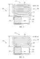
- FIGS. 14 and 15 show a single cell 1400 , such as from the cascaded electrostatic actuators for FIGS. 12 , 13 , 16 , and 17 .
- Each of the cells 1400 of the actuators of FIGS. 12 , 13 , 16 , and 17 can have an un-actuated configuration and an actuated configuration, as discussed below.
- Each cell can be approximately 200 ⁇ m long by approximately 20 ⁇ m wide, for example.
- Each cell can have any desired dimensions.
- Each cell can be generally oval or elongated in shape. Each cell can have any desired shape.
- a single cell 1400 of an actuator is in an un-actuated state (with a voltage off), in accordance with an embodiment.
- the single cell 1400 can comprise a flexure (not illustrated), an isolated plate 1301 , and a pair of surrounding substrate plates 1302 .
- the circumferential gap 1307 can have a substantially uniform width.
- a single cell 1400 of a cascaded electrostatic actuator is in an actuated state (with a voltage on), in accordance with an embodiment.
- the cell 1400 has contracted such that central portions 1405 of the substrate plates 1302 are closer to, e.g. touching or almost touching, the isolated plate 1301 .
- the gap 1307 is still defined, however, at end portions 1403 .
- the isolated plate 1301 and/or the surrounding substrate plates 1302 can have an insulator, e.g., an oxide layer (not shown) formed thereon to electrically insulate the isolated plate 1301 from the surrounding plates 1302 and thus prevent shorting of the electrostatic actuator.
- an insulator e.g., an oxide layer (not shown) formed thereon to electrically insulate the isolated plate 1301 from the surrounding plates 1302 and thus prevent shorting of the electrostatic actuator.
- FIGS. 16 and 17 show a plurality of cells 1400 that are fabricated together so as to define a stack 1600 for a cascaded electrostatic actuator. Any desired number of cells 1400 in any desired configuration can be used to define the stack 1600 .
- the stack 1600 can have any desired number of cells 1400 in a row and can have any desired width.
- the stack 1600 can have any desired number of cells 1400 in a column and can have any desired height.
- FIG. 16 shows a plurality of cells 1400 of a stack 1600 of a cascaded electrostatic actuator in an unactuated state (with a voltage off), in accordance with an embodiment.
- the isolated plates 1301 and the corresponding substrate plates 1302 of each of the cells 1400 are substantially straight and parallel with respect to one another.
- the plates 1301 and 1302 can be crooked and/or non-parallel with respect to one another.
- the cells 1400 of the stack 1600 can be somewhat analogous to the cells of a muscle. Providing more cells can provide more travel and/or more force. Generally, providing more cells 1400 in each column will provide more travel and providing more cells 1400 in each row will provide more force.
- the cells 1400 are in a staggered configuration. That is, adjacent columns of cells 1400 overlap substantially with respect to one another. Alternatively, the cells 1400 can have a non-staggered configuration.
- the cells 1400 are staggered so as to have approximately 50% overlap.
- the cells 1400 can be staggered in a different fashion, so as to have any desired amount of overlap.
- the cells 1400 can have 20% overlap, 25% overlap, 33.3% overlap, or any other amount of overlap.
- the stack 1600 is at approximately its full height, e.g., is approximately fully extended. Since the voltage is off and no charge is being applied to plates 1301 and 1302 , the stack has not contracted.
- FIG. 17 shows a plurality of cells 1400 of a stack 1600 of a cascaded electrostatic actuator in an actuated state (with a voltage on), in accordance with an embodiment.
- the surrounding plates 1302 for each of the cells 1400 is substantially curved inwardly toward the isolated plate 1301 (as shown also in FIG. 15 ).
- Each of the cells 1400 is fully contracted.
- the stack 1600 is at approximately its shortest height, e.g., is approximately fully contracted. Note that as compared to the serpentine embodiments discussed earlier, stack 1600 has just one-half the travel since the overlapped ends of each cell cannot contract.
- cells 1400 may be made electrically independent of each other by having paths of polysilicon of other conductive leads patterned to define conductors to just certain ones or groups of cells.
- an isolated plate embodiment offers attractive selective actuation capabilities as compared to a serpentine embodiment.
- FIG. 17 shows all of the cells 1400 in an actuated or fully contracted state, some of the cells 1400 can alternatively remain in an unactuated state due to the selective capability of an isolated plate embodiment. In this manner, the height of the stack 1600 can be more precisely controlled. For example, every other row of the cells 1400 can be actuated to provide approximately one half of the total travel of the actuator.
- the stack can be made to curve by actuating some cells 1400 while not actuating other cells 1400 .
- the cells 1400 on the left side of the stack 1600 can be actuated while the cells 1400 on the right side of the stack 1600 are not actuated to cause the stack 1600 to bend to the left. Additional details regarding cascaded actuators are disclosed in the incorporated-by-reference Cascaded Electrostatic Actuator U.S. patent application.
- controller 203 may be configured to command an application of a sufficiently high voltage such as 30 V across the various gaps in the cascaded electrostatic stack to snap-in all the gaps and collapse cascaded electrostatic actuator 102 to it fully actuated state. Conversely, should controller 203 apply a voltage of 0 V across all gaps, actuator 102 may relax to its un-actuated height. Actuator 102 in such an embodiment would be essentially a two-position actuator.
- the serpentine folds may be of varying length such that the stack forms a trapezoidal shape.
- An analogous length variation may be implemented in an isolated plate cascaded electrostatic actuator embodiment. Regardless of the actuator type, the varying lengths of the resulting plate pairs thus have varying resistances to snap-in. Once a given gap has closed, the resulting greatly increased electrostatic attraction will maintain the gap closed at voltages lower than that required for the initial snap-in. There is thus hysteresis with respect to the voltages for snap-in versus the voltage at which closed gaps open.
- the resulting serpentine cascaded actuator may thus be selectively actuated across various intermediate positions between closure of all gaps and having all gaps completely relaxed. Each gap will snap-in at differing voltages. The more flexible plates will snap-in at lower voltages whereas the stiffer plates will snap-in at higher voltages. The gaps will then open at correspondingly lower voltages according to the actuator's hysteresis. The resulting actuator could then be controlled responsive to this hysteresis.
- controller 203 may control a variable serpentine cascaded actuator as shown by FIG. 18 .
- the actuator can be selectively actuated over a range of intermediate positions to contract from a relaxed position (O ⁇ m) to a fully actuated position (100 ⁇ m).
- the various voltage may be stored in a memory or look-up table within controller 203 .
- an initial gap closes at the initial snap-in voltage.
- the actuator travel is thus approximately 5 ⁇ m for that initial gap closure.
- additional gaps are closed such that the full travel of 100 ⁇ m is achieved at 30 V.
- the look-up table For example, to relax the initial gap closure, the voltage would be decreased as shown by path A to place the actuator back into the completely un-actuated state.
- the serpentine cascaded electrostatic actuator may be configured to have the travel versus voltage behavior shown in FIG. 19 .
- the initial snap-out voltage After the actuator has been completely actuated, there is a voltage at which the actuator will relax an initial gap, which is designated herein as the initial snap-out voltage.
- the initial snap-out voltage In the embodiment of FIG. 19 , there is a gap between the initial snap-in voltage and the initial snap-out voltage.
- the voltage control behavior shown in FIG. 18 has no such gap. Because of the gap, a controller could use a voltage within the gap (e.g., 15V) to maintain a given position.
- controller 203 controls the cascaded actuator analogously to a linear stepper motor.
- controller 203 commands high voltage pulses (e.g., 30V) to close gaps sequentially.
- high voltage pulses e.g., 30V
- a gap closes corresponding to each high pulse in FIG. 20 a .
- controller 203 commands low voltage pulses (e.g, 0V) to open gaps sequentially.
Landscapes
- Micromachines (AREA)
Abstract
Description
Claims (18)
Priority Applications (1)
| Application Number | Priority Date | Filing Date | Title |
|---|---|---|---|
| US13/247,919 US8853975B2 (en) | 2011-09-28 | 2011-09-28 | Electrostatic actuator control |
Applications Claiming Priority (1)
| Application Number | Priority Date | Filing Date | Title |
|---|---|---|---|
| US13/247,919 US8853975B2 (en) | 2011-09-28 | 2011-09-28 | Electrostatic actuator control |
Publications (2)
| Publication Number | Publication Date |
|---|---|
| US20130076274A1 US20130076274A1 (en) | 2013-03-28 |
| US8853975B2 true US8853975B2 (en) | 2014-10-07 |
Family
ID=47910557
Family Applications (1)
| Application Number | Title | Priority Date | Filing Date |
|---|---|---|---|
| US13/247,919 Active 2032-05-31 US8853975B2 (en) | 2011-09-28 | 2011-09-28 | Electrostatic actuator control |
Country Status (1)
| Country | Link |
|---|---|
| US (1) | US8853975B2 (en) |
Cited By (1)
| Publication number | Priority date | Publication date | Assignee | Title |
|---|---|---|---|---|
| US9817206B2 (en) | 2012-03-10 | 2017-11-14 | Digitaloptics Corporation | MEMS auto focus miniature camera module with fixed and movable lens groups |
Citations (89)
| Publication number | Priority date | Publication date | Assignee | Title |
|---|---|---|---|---|
| US4333722A (en) | 1980-12-22 | 1982-06-08 | Eastman Kodak Company | Method of controlling electromagnetic actuator in a camera, and actuator controllable thereby |
| US4384778A (en) | 1981-11-09 | 1983-05-24 | Eastman Kodak Company | Integral, planar electromagnetic camera element/actuator |
| US4408857A (en) | 1982-03-22 | 1983-10-11 | Eastman Kodak Company | Method and circuit for controlling an electromagnetic actuator in photographic apparatus |
| US4496217A (en) | 1980-11-28 | 1985-01-29 | Canon Kabushiki Kaisha | Actuating device for photographic lens assembly |
| US4716432A (en) | 1986-04-24 | 1987-12-29 | Eastman Kodak Company | Exposure control apparatus |
| US4860040A (en) | 1987-06-19 | 1989-08-22 | Canon Kabushiki Kaisha | Camera |
| US5150260A (en) | 1990-10-02 | 1992-09-22 | Canon Kabushiki Kaisha | Optical apparatus |
| US5386294A (en) | 1990-07-05 | 1995-01-31 | Nikon Corporation | Pattern position measuring apparatus |
| US5699621A (en) | 1996-02-21 | 1997-12-23 | Massachusetts Institute Of Technology | Positioner with long travel in two dimensions |
| US5825560A (en) | 1995-02-28 | 1998-10-20 | Canon Kabushiki Xaisha | Optical apparatus |
| US5986826A (en) | 1996-12-17 | 1999-11-16 | Minolta Co., Ltd. | Drive device using electromechanical conversion element |
| US6033131A (en) | 1998-09-30 | 2000-03-07 | Eastman Kodak Company | Hybrid silicon-based micro-electromagnetic light shutter |
| US6068801A (en) | 1996-12-19 | 2000-05-30 | Telefonaktiebolaget Lm Ericsson | Method for making elastic bumps from a wafer mold having grooves |
| US6205267B1 (en) | 1998-11-20 | 2001-03-20 | Lucent Technologies | Optical switch |
| US20010004420A1 (en) | 1999-12-17 | 2001-06-21 | Minolta Co., Ltd. | Driving system with elastically supporting units |
| US6262827B1 (en) | 1999-06-29 | 2001-07-17 | Fujitsu Limited | Galvano-mirror |
| US20020006687A1 (en) | 2000-05-23 | 2002-01-17 | Lam Ken M. | Integrated IC chip package for electronic image sensor die |
| US6392703B1 (en) | 1995-02-28 | 2002-05-21 | Canon Kabushiki Kaisha | Optical apparatus for forming an object image on a sensing element |
| US20020070634A1 (en) | 2000-09-25 | 2002-06-13 | Yu-Chong Tai | Freestanding polymer MEMS structures with anti stiction |
| US6426777B1 (en) | 1997-04-03 | 2002-07-30 | Asahi Kogaku Kogyo Kabushiki Kaisha | Hybrid camera selectively using either silver-halide-type photographic film or photoelectric-conversion-type image sensor |
| US20020105699A1 (en) * | 2001-02-02 | 2002-08-08 | Teravicta Technologies, Inc | Integrated optical micro-electromechanical systems and methods of fabricating and operating the same |
| US20020125789A1 (en) | 2001-03-07 | 2002-09-12 | Jobst Brandt | Micro-mover with balanced dynamics |
| US6497141B1 (en) | 1999-06-07 | 2002-12-24 | Cornell Research Foundation Inc. | Parametric resonance in microelectromechanical structures |
| US20030048036A1 (en) | 2001-08-31 | 2003-03-13 | Lemkin Mark Alan | MEMS comb-finger actuator |
| US6535311B1 (en) | 1999-12-09 | 2003-03-18 | Corning Incorporated | Wavelength selective cross-connect switch using a MEMS shutter array |
| US20030062422A1 (en) | 2001-09-10 | 2003-04-03 | Fateley William G. | System and method for encoded spatio-spectral information processing |
| US20030076421A1 (en) | 2001-10-19 | 2003-04-24 | Nokia Corporation | Image stabilizer for a microcamera module of a handheld device, and method for stabilizing a microcamera module of a handheld device |
| US20030086751A1 (en) | 2001-11-08 | 2003-05-08 | Culpepper Martin L | Multiple degree of freedom compliant mechanism |
| US6621134B1 (en) * | 2002-02-07 | 2003-09-16 | Shayne Zurn | Vacuum sealed RF/microwave microresonator |
| US20030210116A1 (en) | 2002-05-08 | 2003-11-13 | Motorola, Inc. | Micro electro-mechanical system with one or more moving parts method and apparatus |
| US6674383B2 (en) | 2000-11-01 | 2004-01-06 | Onix Microsystems, Inc. | PWM-based measurement interface for a micro-machined electrostatic actuator |
| US6675671B1 (en) | 2002-05-22 | 2004-01-13 | Sandia Corporation | Planar-constructed spatial micro-stage |
| US20040048410A1 (en) | 2002-09-09 | 2004-03-11 | Motorola Inc. | SOI polysilicon trench refill perimeter oxide anchor scheme |
| US20040066494A1 (en) | 2002-08-30 | 2004-04-08 | Samsung Electronics, Co., Ltd. | Highly efficient scrolling projection system and method |
| US20040142509A1 (en) * | 2002-09-24 | 2004-07-22 | Seiko Epson Corporation | Semiconductor device and method of manufacturing the same, circuit board, and electronic instrument |
| US20040183936A1 (en) | 2003-03-18 | 2004-09-23 | Young-Jun Kim | Digital camera module, apparatus and method of assembling the same |
| US20040189969A1 (en) | 2003-03-14 | 2004-09-30 | Makoto Mizuno | Drive mechanism, exposure device, optical equipment, and device manufacturing method |
| US20040201773A1 (en) | 2001-02-08 | 2004-10-14 | Toni Ostergard | Microminiature zoom system for digital camera |
| US20050002086A1 (en) | 2000-10-31 | 2005-01-06 | Microsoft Corporation | Microelectrical mechanical structure (MEMS) optical modulator and optical display system |
| US20050002008A1 (en) | 2003-05-06 | 2005-01-06 | Asml Netherlands B.V. | Lithographic apparatus, device manufacturing method and device manufactured thereby |
| US20050007489A1 (en) | 2003-07-08 | 2005-01-13 | Lg Electronics Inc. | Rotary camera assembly of mobile communication device |
| US6847907B1 (en) | 2002-12-31 | 2005-01-25 | Active Optical Networks, Inc. | Defect detection and repair of micro-electro-mechanical systems (MEMS) devices |
| US6850675B1 (en) | 2002-02-04 | 2005-02-01 | Siwave, Inc. | Base, payload and connecting structure and methods of making the same |
| US20050095813A1 (en) | 2003-11-05 | 2005-05-05 | Xu Zhu | Ultrathin form factor MEMS microphones and microspeakers |
| US20050139542A1 (en) | 2001-10-22 | 2005-06-30 | Dickensheets David L. | Stiffened surface micromachined structures and process for fabricating the same |
| US20050148433A1 (en) | 2003-12-31 | 2005-07-07 | Shen-Tai Industry Co., Ltd. | Water trampoline |
| US20050219399A1 (en) | 2004-03-30 | 2005-10-06 | Fuji Photo Film Co., Ltd | Image capture apparatus |
| US6958777B1 (en) | 2000-09-29 | 2005-10-25 | Ess Technology, Inc. | Exposure control in electromechanical imaging devices |
| US20050249487A1 (en) | 2004-03-12 | 2005-11-10 | Gutierrez Roman C | Miniature camera |
| US20060028320A1 (en) | 2004-08-09 | 2006-02-09 | Mitsumi Electric Co., Ltd. | Autofocus actuator |
| US20060033938A1 (en) | 2004-08-12 | 2006-02-16 | Kopf Dale R | Image-forming apparatus |
| US7027206B2 (en) | 2004-01-26 | 2006-04-11 | Fuji Photo Film Co., Ltd. | Spatial light modulator, spatial light modulator array, and image formation apparatus |
| US7038150B1 (en) | 2004-07-06 | 2006-05-02 | Sandia Corporation | Micro environmental sensing device |
| US20060183332A1 (en) | 2005-02-14 | 2006-08-17 | Samsung Electronics Co., Ltd. | Method of manufacturing floating structure |
| US20060192858A1 (en) | 2005-02-28 | 2006-08-31 | Calvet Robert J | Oil damping for camera optical assembly |
| US20060193618A1 (en) | 2005-02-28 | 2006-08-31 | Calvet Robert J | Axial snubbers for camera |
| US20060204242A1 (en) | 2005-02-28 | 2006-09-14 | Gutierrez Roman C | Autofocus camera |
| US20060209012A1 (en) | 2005-02-23 | 2006-09-21 | Pixtronix, Incorporated | Devices having MEMS displays |
| US20060219006A1 (en) | 2003-10-20 | 2006-10-05 | Nasiri Steven S | Method of making an X-Y axis dual-mass tuning fork gyroscope with vertically integrated electronics and wafer-scale hermetic packaging |
| US20060250325A1 (en) | 2005-02-23 | 2006-11-09 | Pixtronix, Incorporated | Display methods and apparatus |
| US7154199B2 (en) | 2004-12-24 | 2006-12-26 | Canon Kabushiki Kaisha | Driving apparatus for moving member to be moved |
| US7185542B2 (en) * | 2001-12-06 | 2007-03-06 | Microfabrica Inc. | Complex microdevices and apparatus and methods for fabricating such devices |
| US7203552B2 (en) * | 2000-07-14 | 2007-04-10 | Solvisions Technologies International Inc. | Method and apparatus for controlling a deformable mirror |
| US20070133976A1 (en) | 2005-02-28 | 2007-06-14 | Gutierrez Roman C | Shutter for miniature camera |
| US20080020573A1 (en) | 2004-10-21 | 2008-01-24 | Jeffrey Birkmeyer | Sacrificial substrate for etching |
| US20080044172A1 (en) | 2005-02-28 | 2008-02-21 | Tang Tony K | Lens barrel assembly |
| US7368846B2 (en) * | 2002-11-06 | 2008-05-06 | Matsushita Electric Industrial Co., Ltd. | Microactuator with displacement sensing function and deformable mirror including the microactuator |
| US7372074B2 (en) | 2005-10-11 | 2008-05-13 | Honeywell International, Inc. | Surface preparation for selective silicon fusion bonding |
| US7372616B2 (en) * | 2001-12-06 | 2008-05-13 | Microfabrica, Inc. | Complex microdevices and apparatus and methods for fabricating such devices |
| US7389021B2 (en) * | 2004-04-27 | 2008-06-17 | Marc Epitaux | Movable lens beam steerer |
| US20080239455A1 (en) * | 2007-03-28 | 2008-10-02 | Lior Kogut | Microelectromechanical device and method utilizing conducting layers separated by stops |
| US7545591B1 (en) | 2006-10-17 | 2009-06-09 | Siimpel Corporation | Uniform wall thickness lens barrel |
| US7646969B2 (en) | 2005-02-28 | 2010-01-12 | Siimpel Corporation | Camera snubber assembly |
| US7705909B2 (en) | 2006-08-31 | 2010-04-27 | Mitsumi Electric Co., Ltd. | Camera module with improved leaf spring attachment |
| US7720366B2 (en) | 2006-05-08 | 2010-05-18 | Tamron Co., Ltd | Actuator, and lens unit and camera with the same |
| US7749792B2 (en) * | 2004-06-02 | 2010-07-06 | Carnegie Mellon University | Self-assembling MEMS devices having thermal actuation |
| US20100232777A1 (en) | 2009-03-13 | 2010-09-16 | Largan Precision Co., Ltd. | Photographing module |
| US20100284081A1 (en) | 2009-05-08 | 2010-11-11 | Gutierrez Roman C | Integrated lens barrel |
| US7838322B1 (en) | 2005-02-28 | 2010-11-23 | Tessera MEMS Technologies, Inc. | Method of enhancing an etch system |
| US20110026148A1 (en) | 2008-04-08 | 2011-02-03 | Konica Minolta Holdings, Inc. | Actuator array sheet |
| US20110177745A1 (en) * | 2006-01-13 | 2011-07-21 | Qualcomm Mems Technologies, Inc. | Interconnect structure for mems device |
| US7990628B1 (en) | 2007-08-29 | 2011-08-02 | Tessera MEMS Technologies, Inc. | Planar flexure system with high pitch stiffness |
| US8068521B2 (en) * | 2008-01-17 | 2011-11-29 | Daylight Solutions, Inc. | Laser source that generates a plurality of alternative wavelength output beams |
| US8138859B2 (en) * | 2008-04-21 | 2012-03-20 | Formfactor, Inc. | Switch for use in microelectromechanical systems (MEMS) and MEMS devices incorporating same |
| US8337103B2 (en) * | 2010-11-15 | 2012-12-25 | DigitalOptics Corporation MEMS | Long hinge actuator snubbing |
| US8358925B2 (en) * | 2010-11-15 | 2013-01-22 | DigitalOptics Corporation MEMS | Lens barrel with MEMS actuators |
| US8430580B2 (en) * | 2010-11-15 | 2013-04-30 | DigitalOptics Corporation MEMS | Rotationally deployed actuators |
| US8521017B2 (en) * | 2010-11-15 | 2013-08-27 | DigitalOptics Corporation MEMS | MEMS actuator alignment |
| US8547627B2 (en) * | 2010-11-15 | 2013-10-01 | DigitalOptics Corporation MEMS | Electrical routing |
-
2011
- 2011-09-28 US US13/247,919 patent/US8853975B2/en active Active
Patent Citations (97)
| Publication number | Priority date | Publication date | Assignee | Title |
|---|---|---|---|---|
| US4496217A (en) | 1980-11-28 | 1985-01-29 | Canon Kabushiki Kaisha | Actuating device for photographic lens assembly |
| US4333722A (en) | 1980-12-22 | 1982-06-08 | Eastman Kodak Company | Method of controlling electromagnetic actuator in a camera, and actuator controllable thereby |
| US4384778A (en) | 1981-11-09 | 1983-05-24 | Eastman Kodak Company | Integral, planar electromagnetic camera element/actuator |
| US4408857A (en) | 1982-03-22 | 1983-10-11 | Eastman Kodak Company | Method and circuit for controlling an electromagnetic actuator in photographic apparatus |
| US4716432A (en) | 1986-04-24 | 1987-12-29 | Eastman Kodak Company | Exposure control apparatus |
| US4860040A (en) | 1987-06-19 | 1989-08-22 | Canon Kabushiki Kaisha | Camera |
| US5386294A (en) | 1990-07-05 | 1995-01-31 | Nikon Corporation | Pattern position measuring apparatus |
| US5150260A (en) | 1990-10-02 | 1992-09-22 | Canon Kabushiki Kaisha | Optical apparatus |
| US6392703B1 (en) | 1995-02-28 | 2002-05-21 | Canon Kabushiki Kaisha | Optical apparatus for forming an object image on a sensing element |
| US5825560A (en) | 1995-02-28 | 1998-10-20 | Canon Kabushiki Xaisha | Optical apparatus |
| US5699621A (en) | 1996-02-21 | 1997-12-23 | Massachusetts Institute Of Technology | Positioner with long travel in two dimensions |
| US5986826A (en) | 1996-12-17 | 1999-11-16 | Minolta Co., Ltd. | Drive device using electromechanical conversion element |
| US6068801A (en) | 1996-12-19 | 2000-05-30 | Telefonaktiebolaget Lm Ericsson | Method for making elastic bumps from a wafer mold having grooves |
| US6426777B1 (en) | 1997-04-03 | 2002-07-30 | Asahi Kogaku Kogyo Kabushiki Kaisha | Hybrid camera selectively using either silver-halide-type photographic film or photoelectric-conversion-type image sensor |
| US6033131A (en) | 1998-09-30 | 2000-03-07 | Eastman Kodak Company | Hybrid silicon-based micro-electromagnetic light shutter |
| US6205267B1 (en) | 1998-11-20 | 2001-03-20 | Lucent Technologies | Optical switch |
| US6497141B1 (en) | 1999-06-07 | 2002-12-24 | Cornell Research Foundation Inc. | Parametric resonance in microelectromechanical structures |
| US6262827B1 (en) | 1999-06-29 | 2001-07-17 | Fujitsu Limited | Galvano-mirror |
| US6535311B1 (en) | 1999-12-09 | 2003-03-18 | Corning Incorporated | Wavelength selective cross-connect switch using a MEMS shutter array |
| US20010004420A1 (en) | 1999-12-17 | 2001-06-21 | Minolta Co., Ltd. | Driving system with elastically supporting units |
| US20020006687A1 (en) | 2000-05-23 | 2002-01-17 | Lam Ken M. | Integrated IC chip package for electronic image sensor die |
| US7203552B2 (en) * | 2000-07-14 | 2007-04-10 | Solvisions Technologies International Inc. | Method and apparatus for controlling a deformable mirror |
| US20020070634A1 (en) | 2000-09-25 | 2002-06-13 | Yu-Chong Tai | Freestanding polymer MEMS structures with anti stiction |
| US6958777B1 (en) | 2000-09-29 | 2005-10-25 | Ess Technology, Inc. | Exposure control in electromechanical imaging devices |
| US20050002086A1 (en) | 2000-10-31 | 2005-01-06 | Microsoft Corporation | Microelectrical mechanical structure (MEMS) optical modulator and optical display system |
| US6674383B2 (en) | 2000-11-01 | 2004-01-06 | Onix Microsystems, Inc. | PWM-based measurement interface for a micro-machined electrostatic actuator |
| US20020105699A1 (en) * | 2001-02-02 | 2002-08-08 | Teravicta Technologies, Inc | Integrated optical micro-electromechanical systems and methods of fabricating and operating the same |
| US6914635B2 (en) | 2001-02-08 | 2005-07-05 | Nokia Mobile Phones, Ltd. | Microminiature zoom system for digital camera |
| US20040201773A1 (en) | 2001-02-08 | 2004-10-14 | Toni Ostergard | Microminiature zoom system for digital camera |
| US20020125789A1 (en) | 2001-03-07 | 2002-09-12 | Jobst Brandt | Micro-mover with balanced dynamics |
| US20030048036A1 (en) | 2001-08-31 | 2003-03-13 | Lemkin Mark Alan | MEMS comb-finger actuator |
| US20030062422A1 (en) | 2001-09-10 | 2003-04-03 | Fateley William G. | System and method for encoded spatio-spectral information processing |
| US20030076421A1 (en) | 2001-10-19 | 2003-04-24 | Nokia Corporation | Image stabilizer for a microcamera module of a handheld device, and method for stabilizing a microcamera module of a handheld device |
| US20050139542A1 (en) | 2001-10-22 | 2005-06-30 | Dickensheets David L. | Stiffened surface micromachined structures and process for fabricating the same |
| US20030086751A1 (en) | 2001-11-08 | 2003-05-08 | Culpepper Martin L | Multiple degree of freedom compliant mechanism |
| US7185542B2 (en) * | 2001-12-06 | 2007-03-06 | Microfabrica Inc. | Complex microdevices and apparatus and methods for fabricating such devices |
| US20090015903A1 (en) * | 2001-12-06 | 2009-01-15 | Microfabrica Inc. | Complex Microdevices and Apparatus and Methods for Fabricating Such Devices |
| US7372616B2 (en) * | 2001-12-06 | 2008-05-13 | Microfabrica, Inc. | Complex microdevices and apparatus and methods for fabricating such devices |
| US7266272B1 (en) | 2002-02-04 | 2007-09-04 | Siimpel Corporation | Motion control stages and methods of making the same |
| US6850675B1 (en) | 2002-02-04 | 2005-02-01 | Siwave, Inc. | Base, payload and connecting structure and methods of making the same |
| US7113688B2 (en) | 2002-02-04 | 2006-09-26 | Siimpel Corporation | Base, payload and connecting structure and methods of making the same |
| US6621134B1 (en) * | 2002-02-07 | 2003-09-16 | Shayne Zurn | Vacuum sealed RF/microwave microresonator |
| US20030210116A1 (en) | 2002-05-08 | 2003-11-13 | Motorola, Inc. | Micro electro-mechanical system with one or more moving parts method and apparatus |
| US6675671B1 (en) | 2002-05-22 | 2004-01-13 | Sandia Corporation | Planar-constructed spatial micro-stage |
| US20040066494A1 (en) | 2002-08-30 | 2004-04-08 | Samsung Electronics, Co., Ltd. | Highly efficient scrolling projection system and method |
| US20040048410A1 (en) | 2002-09-09 | 2004-03-11 | Motorola Inc. | SOI polysilicon trench refill perimeter oxide anchor scheme |
| US20040142509A1 (en) * | 2002-09-24 | 2004-07-22 | Seiko Epson Corporation | Semiconductor device and method of manufacturing the same, circuit board, and electronic instrument |
| US7635939B2 (en) * | 2002-11-06 | 2009-12-22 | Panasonic Corporation | Microactuator with displacement sensing function and deformable mirror including the microactuator |
| US7368846B2 (en) * | 2002-11-06 | 2008-05-06 | Matsushita Electric Industrial Co., Ltd. | Microactuator with displacement sensing function and deformable mirror including the microactuator |
| US6847907B1 (en) | 2002-12-31 | 2005-01-25 | Active Optical Networks, Inc. | Defect detection and repair of micro-electro-mechanical systems (MEMS) devices |
| US20040189969A1 (en) | 2003-03-14 | 2004-09-30 | Makoto Mizuno | Drive mechanism, exposure device, optical equipment, and device manufacturing method |
| US20040183936A1 (en) | 2003-03-18 | 2004-09-23 | Young-Jun Kim | Digital camera module, apparatus and method of assembling the same |
| US20050002008A1 (en) | 2003-05-06 | 2005-01-06 | Asml Netherlands B.V. | Lithographic apparatus, device manufacturing method and device manufactured thereby |
| US20050007489A1 (en) | 2003-07-08 | 2005-01-13 | Lg Electronics Inc. | Rotary camera assembly of mobile communication device |
| US20060219006A1 (en) | 2003-10-20 | 2006-10-05 | Nasiri Steven S | Method of making an X-Y axis dual-mass tuning fork gyroscope with vertically integrated electronics and wafer-scale hermetic packaging |
| US20050095813A1 (en) | 2003-11-05 | 2005-05-05 | Xu Zhu | Ultrathin form factor MEMS microphones and microspeakers |
| US20050148433A1 (en) | 2003-12-31 | 2005-07-07 | Shen-Tai Industry Co., Ltd. | Water trampoline |
| US7027206B2 (en) | 2004-01-26 | 2006-04-11 | Fuji Photo Film Co., Ltd. | Spatial light modulator, spatial light modulator array, and image formation apparatus |
| US20050249487A1 (en) | 2004-03-12 | 2005-11-10 | Gutierrez Roman C | Miniature camera |
| US20050219399A1 (en) | 2004-03-30 | 2005-10-06 | Fuji Photo Film Co., Ltd | Image capture apparatus |
| US7389021B2 (en) * | 2004-04-27 | 2008-06-17 | Marc Epitaux | Movable lens beam steerer |
| US7749792B2 (en) * | 2004-06-02 | 2010-07-06 | Carnegie Mellon University | Self-assembling MEMS devices having thermal actuation |
| US7038150B1 (en) | 2004-07-06 | 2006-05-02 | Sandia Corporation | Micro environmental sensing device |
| US20060028320A1 (en) | 2004-08-09 | 2006-02-09 | Mitsumi Electric Co., Ltd. | Autofocus actuator |
| US7285879B2 (en) | 2004-08-09 | 2007-10-23 | Mitsumi Electric Co., Ltd. | Autofocus actuator |
| US20060033938A1 (en) | 2004-08-12 | 2006-02-16 | Kopf Dale R | Image-forming apparatus |
| US20080020573A1 (en) | 2004-10-21 | 2008-01-24 | Jeffrey Birkmeyer | Sacrificial substrate for etching |
| US7154199B2 (en) | 2004-12-24 | 2006-12-26 | Canon Kabushiki Kaisha | Driving apparatus for moving member to be moved |
| US20060183332A1 (en) | 2005-02-14 | 2006-08-17 | Samsung Electronics Co., Ltd. | Method of manufacturing floating structure |
| US20060250325A1 (en) | 2005-02-23 | 2006-11-09 | Pixtronix, Incorporated | Display methods and apparatus |
| US20060209012A1 (en) | 2005-02-23 | 2006-09-21 | Pixtronix, Incorporated | Devices having MEMS displays |
| US7555210B2 (en) | 2005-02-28 | 2009-06-30 | Siimpel, Inc. | Axial snubbers for camera |
| US20060193618A1 (en) | 2005-02-28 | 2006-08-31 | Calvet Robert J | Axial snubbers for camera |
| US20080044172A1 (en) | 2005-02-28 | 2008-02-21 | Tang Tony K | Lens barrel assembly |
| US7838322B1 (en) | 2005-02-28 | 2010-11-23 | Tessera MEMS Technologies, Inc. | Method of enhancing an etch system |
| US20070133976A1 (en) | 2005-02-28 | 2007-06-14 | Gutierrez Roman C | Shutter for miniature camera |
| US20060204242A1 (en) | 2005-02-28 | 2006-09-14 | Gutierrez Roman C | Autofocus camera |
| US20060192858A1 (en) | 2005-02-28 | 2006-08-31 | Calvet Robert J | Oil damping for camera optical assembly |
| US7646969B2 (en) | 2005-02-28 | 2010-01-12 | Siimpel Corporation | Camera snubber assembly |
| US7372074B2 (en) | 2005-10-11 | 2008-05-13 | Honeywell International, Inc. | Surface preparation for selective silicon fusion bonding |
| US20110177745A1 (en) * | 2006-01-13 | 2011-07-21 | Qualcomm Mems Technologies, Inc. | Interconnect structure for mems device |
| US7720366B2 (en) | 2006-05-08 | 2010-05-18 | Tamron Co., Ltd | Actuator, and lens unit and camera with the same |
| US7705909B2 (en) | 2006-08-31 | 2010-04-27 | Mitsumi Electric Co., Ltd. | Camera module with improved leaf spring attachment |
| US7545591B1 (en) | 2006-10-17 | 2009-06-09 | Siimpel Corporation | Uniform wall thickness lens barrel |
| US7742220B2 (en) * | 2007-03-28 | 2010-06-22 | Qualcomm Mems Technologies, Inc. | Microelectromechanical device and method utilizing conducting layers separated by stops |
| US20080239455A1 (en) * | 2007-03-28 | 2008-10-02 | Lior Kogut | Microelectromechanical device and method utilizing conducting layers separated by stops |
| US7990628B1 (en) | 2007-08-29 | 2011-08-02 | Tessera MEMS Technologies, Inc. | Planar flexure system with high pitch stiffness |
| US8068521B2 (en) * | 2008-01-17 | 2011-11-29 | Daylight Solutions, Inc. | Laser source that generates a plurality of alternative wavelength output beams |
| US20110026148A1 (en) | 2008-04-08 | 2011-02-03 | Konica Minolta Holdings, Inc. | Actuator array sheet |
| US8138859B2 (en) * | 2008-04-21 | 2012-03-20 | Formfactor, Inc. | Switch for use in microelectromechanical systems (MEMS) and MEMS devices incorporating same |
| US20100232777A1 (en) | 2009-03-13 | 2010-09-16 | Largan Precision Co., Ltd. | Photographing module |
| US20100284081A1 (en) | 2009-05-08 | 2010-11-11 | Gutierrez Roman C | Integrated lens barrel |
| US8337103B2 (en) * | 2010-11-15 | 2012-12-25 | DigitalOptics Corporation MEMS | Long hinge actuator snubbing |
| US8358925B2 (en) * | 2010-11-15 | 2013-01-22 | DigitalOptics Corporation MEMS | Lens barrel with MEMS actuators |
| US8430580B2 (en) * | 2010-11-15 | 2013-04-30 | DigitalOptics Corporation MEMS | Rotationally deployed actuators |
| US8521017B2 (en) * | 2010-11-15 | 2013-08-27 | DigitalOptics Corporation MEMS | MEMS actuator alignment |
| US8547627B2 (en) * | 2010-11-15 | 2013-10-01 | DigitalOptics Corporation MEMS | Electrical routing |
Non-Patent Citations (7)
| Title |
|---|
| Akihiro Koga et al. "Electrostatic Linear Microactuator Mechanism for Focusing a CCD Camera"; Journal of Lightwave Technology, vol. 17, No. 1: p. 43-47; Jan. 1999. |
| Chapter 2: Electrical Microactuators, Apr. 11, 2005. |
| Fernandez, Daniel, et al., Pulse-Drive and Capacitive Measurement Circuit for MEMS Electrostatic Actuators, Stresa, Italy, Apr. 25-27, 2007. |
| Improving Test Efficiency of MEMS Electrostatic Actuators Using the Agilent E4980A Precision LCR Meter, Agilent Technologies, Inc., Apr. 12, 2007. |
| Measuring Capacitance: Methods (fwd); Apr. 26, 1998 http://www.pupman.com/listarchives/1998/April/msg00625.html. |
| PCT/US 06/07024 Search Report of Nov. 28, 2007. |
| Polymems Actuator: A Polymer-Based Microelectromechanical (MEMS) Actuator with Macroscopic Action, Honeywell International Incorporated, Final Technical Report, Sep. 2002. |
Cited By (1)
| Publication number | Priority date | Publication date | Assignee | Title |
|---|---|---|---|---|
| US9817206B2 (en) | 2012-03-10 | 2017-11-14 | Digitaloptics Corporation | MEMS auto focus miniature camera module with fixed and movable lens groups |
Also Published As
| Publication number | Publication date |
|---|---|
| US20130076274A1 (en) | 2013-03-28 |
Similar Documents
| Publication | Publication Date | Title |
|---|---|---|
| US8869625B2 (en) | MEMS actuator/sensor | |
| KR100941403B1 (en) | Micro rocking device and micro rocking device driving method | |
| US7619349B2 (en) | Piezoelectric driven MEMS device | |
| US6841899B2 (en) | Actuator, actuator driving method, and atcuator system | |
| US10476404B2 (en) | Row and column actuator control | |
| JP2009536015A (en) | Electrostatic actuator | |
| WO2003096388A9 (en) | Micro-mechanical system employing electrostatic actuator and fabrication methods of same | |
| JP2004530172A (en) | Camera / lens positioning device using electro-active element | |
| JP5418317B2 (en) | Electrostatic actuator and driving method thereof | |
| JP4550578B2 (en) | Micro movable element with torsion bar | |
| US7705514B2 (en) | Bi-directional actuator utilizing both attractive and repulsive electrostatic forces | |
| JP2003185406A (en) | Position detecting device | |
| US20200144935A1 (en) | Comb drive with non-parallel overlapping comb fingers | |
| US20190157988A1 (en) | Multi-directional actuator | |
| US8853975B2 (en) | Electrostatic actuator control | |
| US9350271B2 (en) | Cascaded electrostatic actuator | |
| EP2017949A1 (en) | Stepping actuator and method of fabrication | |
| KR100559079B1 (en) | Optical switch and driving method thereof | |
| EP1798195A2 (en) | Comb-type electrode structure capable of large linear-displacement motion | |
| JP5161006B2 (en) | Method for manufacturing electrostatic actuator | |
| CA2485153C (en) | Bi-directional actuator utilizing both attractive and repulsive electrostatic forces | |
| JP5243932B2 (en) | Electrostrictive actuator system | |
| JPH05267741A (en) | Piezoelectric actuator |
Legal Events
| Date | Code | Title | Description |
|---|---|---|---|
| AS | Assignment |
Owner name: DIGITALOPTICS CORPORATION MEMS, CALIFORNIA Free format text: ASSIGNMENT OF ASSIGNORS INTEREST;ASSIGNOR:GUTIERREZ, ROMAN C.;REEL/FRAME:026986/0168 Effective date: 20110922 |
|
| STCF | Information on status: patent grant |
Free format text: PATENTED CASE |
|
| AS | Assignment |
Owner name: ROYAL BANK OF CANADA, AS COLLATERAL AGENT, CANADA Free format text: SECURITY INTEREST;ASSIGNORS:INVENSAS CORPORATION;TESSERA, INC.;TESSERA ADVANCED TECHNOLOGIES, INC.;AND OTHERS;REEL/FRAME:040797/0001 Effective date: 20161201 |
|
| MAFP | Maintenance fee payment |
Free format text: PAYMENT OF MAINTENANCE FEE, 4TH YEAR, LARGE ENTITY (ORIGINAL EVENT CODE: M1551) Year of fee payment: 4 |
|
| AS | Assignment |
Owner name: INVENSAS BONDING TECHNOLOGIES, INC. (F/K/A ZIPTRONIX, INC.), CALIFORNIA Free format text: RELEASE BY SECURED PARTY;ASSIGNOR:ROYAL BANK OF CANADA;REEL/FRAME:052920/0001 Effective date: 20200601 Owner name: DTS, INC., CALIFORNIA Free format text: RELEASE BY SECURED PARTY;ASSIGNOR:ROYAL BANK OF CANADA;REEL/FRAME:052920/0001 Effective date: 20200601 Owner name: DTS LLC, CALIFORNIA Free format text: RELEASE BY SECURED PARTY;ASSIGNOR:ROYAL BANK OF CANADA;REEL/FRAME:052920/0001 Effective date: 20200601 Owner name: INVENSAS CORPORATION, CALIFORNIA Free format text: RELEASE BY SECURED PARTY;ASSIGNOR:ROYAL BANK OF CANADA;REEL/FRAME:052920/0001 Effective date: 20200601 Owner name: FOTONATION CORPORATION (F/K/A DIGITALOPTICS CORPORATION AND F/K/A DIGITALOPTICS CORPORATION MEMS), CALIFORNIA Free format text: RELEASE BY SECURED PARTY;ASSIGNOR:ROYAL BANK OF CANADA;REEL/FRAME:052920/0001 Effective date: 20200601 Owner name: TESSERA ADVANCED TECHNOLOGIES, INC, CALIFORNIA Free format text: RELEASE BY SECURED PARTY;ASSIGNOR:ROYAL BANK OF CANADA;REEL/FRAME:052920/0001 Effective date: 20200601 Owner name: TESSERA, INC., CALIFORNIA Free format text: RELEASE BY SECURED PARTY;ASSIGNOR:ROYAL BANK OF CANADA;REEL/FRAME:052920/0001 Effective date: 20200601 Owner name: IBIQUITY DIGITAL CORPORATION, MARYLAND Free format text: RELEASE BY SECURED PARTY;ASSIGNOR:ROYAL BANK OF CANADA;REEL/FRAME:052920/0001 Effective date: 20200601 Owner name: PHORUS, INC., CALIFORNIA Free format text: RELEASE BY SECURED PARTY;ASSIGNOR:ROYAL BANK OF CANADA;REEL/FRAME:052920/0001 Effective date: 20200601 |
|
| MAFP | Maintenance fee payment |
Free format text: PAYMENT OF MAINTENANCE FEE, 8TH YEAR, LARGE ENTITY (ORIGINAL EVENT CODE: M1552); ENTITY STATUS OF PATENT OWNER: LARGE ENTITY Year of fee payment: 8 |
|
| AS | Assignment |
Owner name: BANK OF AMERICA, N.A., AS COLLATERAL AGENT, NORTH CAROLINA Free format text: SECURITY INTEREST;ASSIGNORS:ADEIA GUIDES INC.;ADEIA IMAGING LLC;ADEIA MEDIA HOLDINGS LLC;AND OTHERS;REEL/FRAME:063529/0272 Effective date: 20230501 |