US8852999B2 - System-in-a-package based flash memory card - Google Patents
System-in-a-package based flash memory card Download PDFInfo
- Publication number
- US8852999B2 US8852999B2 US13/235,852 US201113235852A US8852999B2 US 8852999 B2 US8852999 B2 US 8852999B2 US 201113235852 A US201113235852 A US 201113235852A US 8852999 B2 US8852999 B2 US 8852999B2
- Authority
- US
- United States
- Prior art keywords
- integrated circuit
- package
- chamfer
- card
- flash memory
- Prior art date
- Legal status (The legal status is an assumption and is not a legal conclusion. Google has not performed a legal analysis and makes no representation as to the accuracy of the status listed.)
- Active, expires
Links
Images


Classifications
-
- G—PHYSICS
- G06—COMPUTING OR CALCULATING; COUNTING
- G06K—GRAPHICAL DATA READING; PRESENTATION OF DATA; RECORD CARRIERS; HANDLING RECORD CARRIERS
- G06K19/00—Record carriers for use with machines and with at least a part designed to carry digital markings
- G06K19/06—Record carriers for use with machines and with at least a part designed to carry digital markings characterised by the kind of the digital marking, e.g. shape, nature, code
- G06K19/067—Record carriers with conductive marks, printed circuits or semiconductor circuit elements, e.g. credit or identity cards also with resonating or responding marks without active components
- G06K19/07—Record carriers with conductive marks, printed circuits or semiconductor circuit elements, e.g. credit or identity cards also with resonating or responding marks without active components with integrated circuit chips
- G06K19/077—Constructional details, e.g. mounting of circuits in the carrier
- G06K19/07745—Mounting details of integrated circuit chips
-
- G—PHYSICS
- G06—COMPUTING OR CALCULATING; COUNTING
- G06K—GRAPHICAL DATA READING; PRESENTATION OF DATA; RECORD CARRIERS; HANDLING RECORD CARRIERS
- G06K19/00—Record carriers for use with machines and with at least a part designed to carry digital markings
- G06K19/06—Record carriers for use with machines and with at least a part designed to carry digital markings characterised by the kind of the digital marking, e.g. shape, nature, code
- G06K19/067—Record carriers with conductive marks, printed circuits or semiconductor circuit elements, e.g. credit or identity cards also with resonating or responding marks without active components
- G06K19/07—Record carriers with conductive marks, printed circuits or semiconductor circuit elements, e.g. credit or identity cards also with resonating or responding marks without active components with integrated circuit chips
- G06K19/077—Constructional details, e.g. mounting of circuits in the carrier
- G06K19/0772—Physical layout of the record carrier
- G06K19/07732—Physical layout of the record carrier the record carrier having a housing or construction similar to well-known portable memory devices, such as SD cards, USB or memory sticks
-
- G—PHYSICS
- G11—INFORMATION STORAGE
- G11C—STATIC STORES
- G11C5/00—Details of stores covered by group G11C11/00
- G11C5/02—Disposition of storage elements, e.g. in the form of a matrix array
- G11C5/04—Supports for storage elements, e.g. memory modules; Mounting or fixing of storage elements on such supports
-
- H01L21/565—
-
- H01L23/3107—
-
- H01L25/0657—
-
- H01L25/16—
-
- H—ELECTRICITY
- H10—SEMICONDUCTOR DEVICES; ELECTRIC SOLID-STATE DEVICES NOT OTHERWISE PROVIDED FOR
- H10W—GENERIC PACKAGES, INTERCONNECTIONS, CONNECTORS OR OTHER CONSTRUCTIONAL DETAILS OF DEVICES COVERED BY CLASS H10
- H10W74/00—Encapsulations, e.g. protective coatings
- H10W74/01—Manufacture or treatment
- H10W74/016—Manufacture or treatment using moulds
-
- H—ELECTRICITY
- H10—SEMICONDUCTOR DEVICES; ELECTRIC SOLID-STATE DEVICES NOT OTHERWISE PROVIDED FOR
- H10W—GENERIC PACKAGES, INTERCONNECTIONS, CONNECTORS OR OTHER CONSTRUCTIONAL DETAILS OF DEVICES COVERED BY CLASS H10
- H10W74/00—Encapsulations, e.g. protective coatings
- H10W74/10—Encapsulations, e.g. protective coatings characterised by their shape or disposition
- H10W74/111—Encapsulations, e.g. protective coatings characterised by their shape or disposition the semiconductor body being completely enclosed
-
- H—ELECTRICITY
- H10—SEMICONDUCTOR DEVICES; ELECTRIC SOLID-STATE DEVICES NOT OTHERWISE PROVIDED FOR
- H10W—GENERIC PACKAGES, INTERCONNECTIONS, CONNECTORS OR OTHER CONSTRUCTIONAL DETAILS OF DEVICES COVERED BY CLASS H10
- H10W90/00—Package configurations
-
- H01L2223/5442—
-
- H01L2223/54433—
-
- H01L2223/54473—
-
- H01L2223/54486—
-
- H01L2224/32145—
-
- H01L2224/48225—
-
- H01L2224/97—
-
- H01L2225/0651—
-
- H01L2225/06568—
-
- H01L24/48—
-
- H01L2924/01322—
-
- H01L2924/12041—
-
- H01L2924/14—
-
- H01L2924/1433—
-
- H01L2924/15311—
-
- H01L2924/15312—
-
- H01L2924/15313—
-
- H01L2924/19041—
-
- H01L2924/19043—
-
- H01L2924/19105—
-
- H—ELECTRICITY
- H05—ELECTRIC TECHNIQUES NOT OTHERWISE PROVIDED FOR
- H05K—PRINTED CIRCUITS; CASINGS OR CONSTRUCTIONAL DETAILS OF ELECTRIC APPARATUS; MANUFACTURE OF ASSEMBLAGES OF ELECTRICAL COMPONENTS
- H05K1/00—Printed circuits
- H05K1/18—Printed circuits structurally associated with non-printed electric components
- H05K1/181—Printed circuits structurally associated with non-printed electric components associated with surface mounted components
-
- H—ELECTRICITY
- H05—ELECTRIC TECHNIQUES NOT OTHERWISE PROVIDED FOR
- H05K—PRINTED CIRCUITS; CASINGS OR CONSTRUCTIONAL DETAILS OF ELECTRIC APPARATUS; MANUFACTURE OF ASSEMBLAGES OF ELECTRICAL COMPONENTS
- H05K3/00—Apparatus or processes for manufacturing printed circuits
- H05K3/0011—Working of insulating substrates or insulating layers
- H05K3/0044—Mechanical working of the substrate, e.g. drilling or punching
- H05K3/0052—Depaneling, i.e. dividing a panel into circuit boards; Working of the edges of circuit boards
-
- H—ELECTRICITY
- H10—SEMICONDUCTOR DEVICES; ELECTRIC SOLID-STATE DEVICES NOT OTHERWISE PROVIDED FOR
- H10W—GENERIC PACKAGES, INTERCONNECTIONS, CONNECTORS OR OTHER CONSTRUCTIONAL DETAILS OF DEVICES COVERED BY CLASS H10
- H10W46/00—Marks applied to devices, e.g. for alignment or identification
- H10W46/101—Marks applied to devices, e.g. for alignment or identification characterised by the type of information, e.g. logos or symbols
-
- H—ELECTRICITY
- H10—SEMICONDUCTOR DEVICES; ELECTRIC SOLID-STATE DEVICES NOT OTHERWISE PROVIDED FOR
- H10W—GENERIC PACKAGES, INTERCONNECTIONS, CONNECTORS OR OTHER CONSTRUCTIONAL DETAILS OF DEVICES COVERED BY CLASS H10
- H10W46/00—Marks applied to devices, e.g. for alignment or identification
- H10W46/401—Marks applied to devices, e.g. for alignment or identification for identification or tracking
-
- H—ELECTRICITY
- H10—SEMICONDUCTOR DEVICES; ELECTRIC SOLID-STATE DEVICES NOT OTHERWISE PROVIDED FOR
- H10W—GENERIC PACKAGES, INTERCONNECTIONS, CONNECTORS OR OTHER CONSTRUCTIONAL DETAILS OF DEVICES COVERED BY CLASS H10
- H10W46/00—Marks applied to devices, e.g. for alignment or identification
- H10W46/601—Marks applied to devices, e.g. for alignment or identification for use after dicing
- H10W46/607—Located on parts of packages, e.g. on encapsulations or on package substrates
-
- H—ELECTRICITY
- H10—SEMICONDUCTOR DEVICES; ELECTRIC SOLID-STATE DEVICES NOT OTHERWISE PROVIDED FOR
- H10W—GENERIC PACKAGES, INTERCONNECTIONS, CONNECTORS OR OTHER CONSTRUCTIONAL DETAILS OF DEVICES COVERED BY CLASS H10
- H10W72/00—Interconnections or connectors in packages
- H10W72/01—Manufacture or treatment
- H10W72/0198—Manufacture or treatment batch processes
-
- H—ELECTRICITY
- H10—SEMICONDUCTOR DEVICES; ELECTRIC SOLID-STATE DEVICES NOT OTHERWISE PROVIDED FOR
- H10W—GENERIC PACKAGES, INTERCONNECTIONS, CONNECTORS OR OTHER CONSTRUCTIONAL DETAILS OF DEVICES COVERED BY CLASS H10
- H10W74/00—Encapsulations, e.g. protective coatings
-
- H—ELECTRICITY
- H10—SEMICONDUCTOR DEVICES; ELECTRIC SOLID-STATE DEVICES NOT OTHERWISE PROVIDED FOR
- H10W—GENERIC PACKAGES, INTERCONNECTIONS, CONNECTORS OR OTHER CONSTRUCTIONAL DETAILS OF DEVICES COVERED BY CLASS H10
- H10W90/00—Package configurations
- H10W90/20—Configurations of stacked chips
- H10W90/28—Configurations of stacked chips the stacked chips having different sizes, e.g. chip stacks having a pyramidal shape
-
- H—ELECTRICITY
- H10—SEMICONDUCTOR DEVICES; ELECTRIC SOLID-STATE DEVICES NOT OTHERWISE PROVIDED FOR
- H10W—GENERIC PACKAGES, INTERCONNECTIONS, CONNECTORS OR OTHER CONSTRUCTIONAL DETAILS OF DEVICES COVERED BY CLASS H10
- H10W90/00—Package configurations
- H10W90/701—Package configurations characterised by the relative positions of pads or connectors relative to package parts
- H10W90/731—Package configurations characterised by the relative positions of pads or connectors relative to package parts of die-attach connectors
- H10W90/732—Package configurations characterised by the relative positions of pads or connectors relative to package parts of die-attach connectors between stacked chips
-
- H—ELECTRICITY
- H10—SEMICONDUCTOR DEVICES; ELECTRIC SOLID-STATE DEVICES NOT OTHERWISE PROVIDED FOR
- H10W—GENERIC PACKAGES, INTERCONNECTIONS, CONNECTORS OR OTHER CONSTRUCTIONAL DETAILS OF DEVICES COVERED BY CLASS H10
- H10W90/00—Package configurations
- H10W90/701—Package configurations characterised by the relative positions of pads or connectors relative to package parts
- H10W90/751—Package configurations characterised by the relative positions of pads or connectors relative to package parts of bond wires
- H10W90/754—Package configurations characterised by the relative positions of pads or connectors relative to package parts of bond wires between a chip and a stacked insulating package substrate, interposer or RDL
Definitions
- Embodiments of the present invention relate to a system-in-a-package based flash memory card including an integrated circuit package occupying a small overall area within the card and cut to conform to the shape of a lid for the card.
- Non-volatile semiconductor memory devices such as flash memory storage cards
- flash memory storage cards are becoming widely used to meet the ever-growing demands on digital information storage and exchange.
- Their portability, versatility and rugged design, along with their high reliability and large capacity, have made such memory devices ideal for use in a wide variety of electronic devices.
- SD flash memory card One exemplary standard for flash memory cards is the so-called SD flash memory card.
- the SD (Secure Digital) Card is a secure flash memory about the size of a postage stamp. Jointly developed by SanDisk, Toshiba and Matsushita Electronic (which makes Panasonic products), the SD Card weighs approximately two grams and is used for memory storage in a wide variety of digital products, including for example digital music players, cellular phones, handheld PCs (HPCs), digital cameras, digital video camcorders, smart phones, car navigation systems and electronic books.
- IC integrated circuit
- the individually packaged ICs have been mounted separately on a substrate such as a printed circuit board to form the IC system.
- the printed circuit board took up all or almost all of the available space within the card. The printed circuit board was formed to that size in order to contain all of the individually packaged components.
- SiP system-in-a-package
- MCM multichip modules
- Embodiments of the present invention relate to a system-in-a-package based flash memory card including an integrated circuit (“IC”) package occupying a small overall area within the card and cut to conform to the shape of a lid for the card.
- An integrated circuit may be cut from a panel into a shape that fits within and conforms to the shape of lids for a finished memory card, such as for example an SD Card.
- the integrated circuit package may be a system-in-a-package, a multi-chip module, or other arrangement where a complete electronic system is formed in a single package.
- the IC package is cut with a chamfer that matches up with and conforms to the size and shape of a chamfer formed in a lid for an SD flash memory card.
- the IC package is also cut with a notch that is sized and positioned so as to define a space in which a read/write switch in the SD flash memory card may operate.
- forming all of the IC components within an SiP or similar package provides a significant savings of space within the finished flash memory card in comparison to conventional printed circuit boards including individually packaged components. Whereas the printed circuit board with individually packaged components took up all or substantially all of the available space within a standard SD Card, the IC package takes up less than one-half of the available space in the flash memory card of the present invention.
- FIG. 1 is a flowchart of the method of fabricating a flash memory card according to embodiments of the present invention.
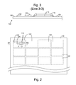
- FIG. 2 is a top view of a panel of integrated circuits during the fabrication process according to the present invention.
- FIG. 3 is a cross-sectional view through line 3 - 3 in FIG. 2 .
- FIG. 4 is a top view of a panel of molded integrated circuits according to embodiments of the present invention prior to being cut into individual integrated circuit packages.
- FIG. 5 is an enlarged view of a pair of integrated circuits with the internal components and cut lines shown.
- FIG. 6 is a top view of an integrated circuit package according to embodiments of the present invention.
- FIG. 7 is an edge view of a first edge of the integrated circuit package according to embodiments of the present invention.
- FIG. 8 is an edge view of a second edge of the integrated circuit package according to embodiments of the present invention.
- FIG. 9 is an edge view of a third edge of the integrated circuit package according to embodiments of the present invention.
- FIG. 10 is an edge view of a fourth edge of the integrated circuit package according to embodiments of the present invention.
- FIG. 11 is a bottom view of an integrated circuit package according to embodiments of the present invention.
- FIG. 12 is a perspective view of a flash memory card including the integrated circuit package of FIG. 6 mounted in a top and bottom lid.
- FIG. 13 is a top view of a flash memory card including the integrated circuit package of FIG. 6 mounted in a top and bottom lid.
- FIG. 14 is a bottom view of a flash memory card including the integrated circuit package of FIG. 6 mounted in a top and bottom lid.
- FIGS. 1 through 14 relate to a system-in-a-package based flash memory card including an integrated circuit package fitting within the footprint of a lid for the package.
- FIGS. 1 through 14 relate to a system-in-a-package based flash memory card including an integrated circuit package fitting within the footprint of a lid for the package.
- the present invention may be embodied in many different forms and should not be construed as being limited to the embodiments set forth herein. Rather, these embodiments are provided so that this disclosure will be thorough and complete and will fully convey the invention to those skilled in the art. Indeed, the invention is intended to cover alternatives, modifications and equivalents of these embodiments, which are included within the scope and spirit of the invention as defined by the appended claims.
- numerous specific details are set forth in order to provide a thorough understanding of the present invention. However, it will be clear to those of ordinary skill in the art that the present invention may be practiced without such specific details.
- panel 100 FIGS. 2 and 3
- the type of panel 100 used in the present invention is not critical and may for example be a substrate in the form of a printed circuit board (“PCB”), a lead frame, a tab automated bonding (“TAB”) tape or other known base on which integrated circuits may be assembled and encapsulated.
- panel 100 may be a PCB substrate formed of a dielectric core having a conductive layer formed on the top and/or bottom surface of the core.
- a conductance pattern may be formed on one or both conductive layers of panel 100 to establish an electrical connection between the components mounted on panel 100 .
- the conductance pattern may further include contact pads, lead fingers or other external connectors for electrical connection between the integrated circuit components and external electronic devices.
- a plurality of discrete integrated circuits 102 may be batch processed on panel 100 to achieve economies of scale. Each of these integrated circuits 102 may then be encapsulated and singulated to form a plurality of integrated circuit packages as explained hereinafter.
- Each integrated circuit 102 being formed on panel 100 may include one or more passive components 104 surface mounted to panel 100 in step 54 .
- the type and number of passive components 104 is not critical to the present invention and may vary widely in alternative embodiments.
- the passive components 104 may include capacitors and/or resistors physically and electrically coupled to panel 100 as is known in the art.
- Embodiments of the present invention may further include a light emitting diode (“LED”) 108 surface mounted to panel 100 in a step 56 .
- the LED 108 may be embedded within the finished package and have an active end emitting light out of an edge of the finished package.
- a package including such an LED is described in U.S. Utility patent application Ser. No. 11/129,637,, entitled “Method Of Assembling Semiconductor Devices With LEDs,” by Takiar et al., filed May 13, 2005, which application has been incorporated by reference herein in its entirety.
- LED 108 may be omitted in embodiments of the invention.
- Each integrated circuit 102 may further include one or more semiconductor die 114 mounted to panel 100 in step 58 in a known adhesive or eutectic die bond process, using a known die-attach compound.
- the number and type of semiconductor die 114 may vary greatly in alternative embodiments of the invention.
- the one or more die 114 may include a flash memory array (e.g., NOR, NAND or other), S-RAM or DDT, and/or a controller chip such as an ASIC. Other semiconductor die are contemplated.
- the one or more die 114 may be electrically connected to panel 100 by wire bonds 116 in step 60 in a known wire-bond process.
- each of the integrated circuits 102 may be encapsulated with a molding compound 120 in step 62 and as shown in FIGS. 3 and 4 .
- Molding compound 120 may be an epoxy available for example, from Nitto Denko Corporation, Osaka, Japan.
- the molding compound may be applied according to various processes, including by transfer molding or flood molding techniques, to form a unitary encapsulation on panel 100 encompassing all of the integrated circuits 102 .
- a marking can be applied to the molding compound 120 in step 64 .
- the marking may for example be a logo or other information printed on the surface of the molding compound for each integrated circuit 102 .
- the marking may for example indicate manufacturer and/or type of device. Marking step 64 may be omitted in alternative embodiments of the present invention.
- Singulation step 66 involves cutting integrated circuits 102 on panel 100 into a plurality of individual integrated circuit packages.
- cutting is used to refer to cutting, sawing, punching or other methods used to separate the integrated circuits 102 into individual integrated circuit packages.
- Known cutting devices include, for example, water jet cutting, laser cutting, water guided laser cutting, dry media cutting, and diamond coated wire.
- Water jet cutting may be the preferred cutting device given its small cutting width (e.g., 50, microns), its ability to shape small features, and its rapid cutting rate. Water can also be used together with laser cutting to help complement or focus its effects.
- each of the integrated circuits may be cut from panel 100 into a shape that fits within and conforms to the shape of lids for a finished memory card as explained in greater detail hereinafter.
- An outline of the cutting shape in one embodiment is shown in dashed lines 118 on the top view of the encapsulated panel in FIG. 4 .
- the integrated circuits 102 are cut from panel 100 so that the one or more die 114 and passive components 106 are entirely contained and enclosed within each singularized package.
- Such a package may form a system-in-a-package (“SiP”).
- the package may alternatively form a multi-chip module (“MCM”) configuration, or other arrangement where a complete electronic system is formed in a single package.
- MCM multi-chip module
- FIG. 6 is a top view of an IC package 126 cut from panel 100 and including integrated circuit 102 encapsulated within molding compound 124 as described above.
- IC package 126 may include a top surface 132 , a first edge 134 , a second edge 136 , a third edge 138 and a fourth edge 140 around a periphery of the package.
- FIGS. 7 through 10 are edge views of the first through fourth edges, respectively, of package 126 .
- IC package 126 may be built as a land grid array (LGA) package.
- LGA land grid array
- Other types of packages, such as pin grid array (PGA) and ball grid array (BGA) packages are contemplated.
- a chamfer 144 is formed in a corner between first edge 134 and fourth edge 140 for conforming to a chamfer in a flash memory card lid as explained in greater detail below.
- a notch 146 may be formed in a corner between second edge 136 and third edge 138 for location of a switch in a flash memory card lid as explained in greater detail below.
- a completed IC package 126 may further be enclosed within an external package or lid (or pair of lids) 150 in step 68 .
- a lid would provide an external covering for the IC package 126 and establish external product features.
- IC package 126 may be shaped for use within an SD Card 152 having a standard SD Card lid configuration and footprint.
- the lid 150 includes a chamfer 154 between a first pair of edges to prevent the card from being improperly inserted into a standard SD card slot on a host device.
- each card slot would include an angled corner which mates with chamfer 154 when card 152 is properly inserted, but would prevent the card 152 from being fully inserted if some other corner of the card 152 was inserted against the angled corner within the host slot.
- IC package 126 includes the chamfer 144 .
- the IC package 126 is cut so that chamfer 144 matches up with and conforms to the size and shape of chamfer 154 .
- standard SD cards are formed with a switch 156 which cooperates with mechanisms in the host device to enable and disable read/write operations from/to the card.
- the IC package 126 is cut so that the notch 146 in package 126 is sized and positioned to not interfere with the switch 156 as it moves between its enable and disable positions.
- IC package 126 provides a significant savings of space within the lids 150 in comparison to conventional printed circuit boards including individually packaged components. Whereas the printed circuit board with individually packaged components took up all or substantially all of the available space within a standard SD Card, the IC package 126 occupies only a fraction of the available space. In an embodiment, IC package 126 may have a maximum length (between the second edge 136 and fourth edge 140 ) of approximately 2, cm, and a maximum width (between the first edge 134 and third edge 138 ) of approximately 1, cm. With these dimensions, the IC package takes up less than one-half of the available space in card 152 . It is understood that the IC package 126 may occupy more than one-half of the available space within card 152 , such as for example three-fourths of the available space in card 152 .
- Embodiments of the present invention have been described including an IC package which fits within the footprint of a standard SD card. However, it is understood that embodiments of the present invention may alternatively shape an SiP, MCM, or other arrangement where a complete electronic system is formed in a single package to fit within an outer lid or enclosure in a number of other flash memory standards. Such standards include but are not limited to a Compact Flash, a Smart Media, a Mini SD Card, an MMC, an xD Card, a Transflash or a Memory Stick. Other devices are contemplated.
- an example of the present technology relates to a method of forming an integrated circuit for a flash memory, the flash memory including one or more lids, the method comprising the steps of: (a) mounting a plurality of integrated circuit components on a base; (b) encapsulating the plurality of integrated circuit components in a molding compound; (c) cutting the encapsulated integrated circuit to a shape to fit within the one or more lids; and (d) cutting the encapsulated integrated circuit to have one or more sides conforming to a shape of the one or more lids.
- the present technology relates to a method of forming an integrated circuit for a flash memory, the flash memory including one or more external lids, the method comprising the steps of: (a) mounting a plurality of integrated circuit components on a substrate; (b) encapsulating the plurality of integrated circuit components in a molding compound; and (c) cutting the encapsulated integrated circuit to include a notch, the notch cut to conform in shape to a notch in the one or more external lids.
- the present technology relates to a method of forming a flash memory, the method comprising the steps of: (a) mounting a plurality of integrated circuit components on a substrate; (b) encapsulating the plurality of integrated circuit components in a molding compound; (c) cutting the encapsulated integrated circuit to include a notch; and (d) encasing the encapsulated integrated circuit within one or more external lids, the one or more external lids including a notch for receiving a reciprocating switch, wherein the notch cut in said step (c) removes a portion of the molding compound that would otherwise interfere with reciprocation of the switch in the notch in the one or more external lids.
Landscapes
- Engineering & Computer Science (AREA)
- Computer Hardware Design (AREA)
- Microelectronics & Electronic Packaging (AREA)
- Physics & Mathematics (AREA)
- General Physics & Mathematics (AREA)
- Theoretical Computer Science (AREA)
- Credit Cards Or The Like (AREA)
Abstract
Description
Claims (9)
Priority Applications (1)
| Application Number | Priority Date | Filing Date | Title |
|---|---|---|---|
| US13/235,852 US8852999B2 (en) | 2005-05-19 | 2011-09-19 | System-in-a-package based flash memory card |
Applications Claiming Priority (2)
| Application Number | Priority Date | Filing Date | Title |
|---|---|---|---|
| US11/133,576 US8022519B2 (en) | 2005-05-19 | 2005-05-19 | System-in-a-package based flash memory card |
| US13/235,852 US8852999B2 (en) | 2005-05-19 | 2011-09-19 | System-in-a-package based flash memory card |
Related Parent Applications (1)
| Application Number | Title | Priority Date | Filing Date |
|---|---|---|---|
| US11/133,576 Division US8022519B2 (en) | 2005-05-19 | 2005-05-19 | System-in-a-package based flash memory card |
Publications (2)
| Publication Number | Publication Date |
|---|---|
| US20120009732A1 US20120009732A1 (en) | 2012-01-12 |
| US8852999B2 true US8852999B2 (en) | 2014-10-07 |
Family
ID=37447587
Family Applications (3)
| Application Number | Title | Priority Date | Filing Date |
|---|---|---|---|
| US11/133,576 Active 2027-03-21 US8022519B2 (en) | 2005-05-19 | 2005-05-19 | System-in-a-package based flash memory card |
| US13/235,852 Active 2026-07-09 US8852999B2 (en) | 2005-05-19 | 2011-09-19 | System-in-a-package based flash memory card |
| US13/235,781 Expired - Fee Related US8637978B2 (en) | 2005-05-19 | 2011-09-19 | System-in-a-package based flash memory card |
Family Applications Before (1)
| Application Number | Title | Priority Date | Filing Date |
|---|---|---|---|
| US11/133,576 Active 2027-03-21 US8022519B2 (en) | 2005-05-19 | 2005-05-19 | System-in-a-package based flash memory card |
Family Applications After (1)
| Application Number | Title | Priority Date | Filing Date |
|---|---|---|---|
| US13/235,781 Expired - Fee Related US8637978B2 (en) | 2005-05-19 | 2011-09-19 | System-in-a-package based flash memory card |
Country Status (1)
| Country | Link |
|---|---|
| US (3) | US8022519B2 (en) |
Cited By (1)
| Publication number | Priority date | Publication date | Assignee | Title |
|---|---|---|---|---|
| US10910233B2 (en) * | 2018-04-11 | 2021-02-02 | Advanced Semiconductor Engineering, Inc. | Semiconductor device package and method of manufacturing the same |
Families Citing this family (19)
| Publication number | Priority date | Publication date | Assignee | Title |
|---|---|---|---|---|
| US8022519B2 (en) * | 2005-05-19 | 2011-09-20 | Sandisk Technologies Inc. | System-in-a-package based flash memory card |
| US20070168566A1 (en) * | 2005-11-07 | 2007-07-19 | Chip Hope Co., Ltd. | Memory card with an indicator light |
| GB0805780D0 (en) * | 2008-03-31 | 2008-04-30 | Royal Bank Of Scotland Plc The | Processor card arrangement |
| CN102074559B (en) * | 2010-11-26 | 2012-11-21 | 天水华天科技股份有限公司 | SiP (Session Initiation Protocol) system integrated-level IC (Integrated Circuit) chip packaging part and manufacturing method thereof |
| US9462705B2 (en) | 2012-10-10 | 2016-10-04 | Sandisk Technologies Llc | USB device with preassembled lid |
| US9888283B2 (en) | 2013-03-13 | 2018-02-06 | Nagrastar Llc | Systems and methods for performing transport I/O |
| USD758372S1 (en) * | 2013-03-13 | 2016-06-07 | Nagrastar Llc | Smart card interface |
| EP2982225A4 (en) | 2013-04-05 | 2017-05-17 | PNY Technologies, Inc. | Reduced length memory card |
| US20160065419A1 (en) * | 2013-04-09 | 2016-03-03 | Nokia Solutions And Networks Oy | Method and apparatus for generating insight into the customer experience of web based applications |
| USD726189S1 (en) * | 2014-04-03 | 2015-04-07 | Transcend Information, Inc. | Secure digital card |
| USD734756S1 (en) * | 2014-04-04 | 2015-07-21 | Pny Technologies, Inc. | Reduced length memory card |
| US20150357280A1 (en) * | 2014-06-06 | 2015-12-10 | Kabushiki Kaisha Toshiba | Memory card and method for manufacturing the same |
| USD864968S1 (en) | 2015-04-30 | 2019-10-29 | Echostar Technologies L.L.C. | Smart card interface |
| JP2017123389A (en) * | 2016-01-06 | 2017-07-13 | 富士通株式会社 | Rigid flexible substrate and manufacturing method thereof |
| US10923462B2 (en) | 2018-05-01 | 2021-02-16 | Western Digital Technologies, Inc. | Bifurcated memory die module semiconductor device |
| US10522489B1 (en) | 2018-06-28 | 2019-12-31 | Western Digital Technologies, Inc. | Manufacturing process for separating logic and memory array |
| KR102834549B1 (en) * | 2020-08-14 | 2025-07-14 | 삼성전자주식회사 | memory card |
| KR102834551B1 (en) * | 2020-12-15 | 2025-07-14 | 삼성전자주식회사 | memory card |
| US20250307593A1 (en) * | 2024-03-28 | 2025-10-02 | Sentrycard Technologies, Inc. | Core layer comprising system-in-package, resulting information carrying card, and methods of making the same |
Citations (28)
| Publication number | Priority date | Publication date | Assignee | Title |
|---|---|---|---|---|
| USD267009S (en) | 1979-04-12 | 1982-11-23 | Sharp Corporation | Magnetic card for microwave oven |
| US5285107A (en) | 1989-04-20 | 1994-02-08 | Sanyo Electric Co., Ltd. | Hybrid integrated circuit device |
| US5808322A (en) | 1997-04-01 | 1998-09-15 | Hewlett-Packard Company | Faster switching GaAs FET switches by illumination with high intensity light |
| USD452690S1 (en) | 1998-04-01 | 2002-01-01 | Sandisk Corporation | Removable memory card for use with portable electronic devices |
| USD452864S1 (en) | 2000-06-12 | 2002-01-08 | Sandisk Corporation | Electronic memory card |
| USD453338S1 (en) | 2001-05-11 | 2002-02-05 | Bank Of America Corporation | Data card |
| US6462273B1 (en) | 2001-03-16 | 2002-10-08 | Micron Technology, Inc. | Semiconductor card and method of fabrication |
| US6567273B1 (en) | 2002-02-06 | 2003-05-20 | Carry Computer Eng. Co., Ltd. | Small silicon disk card with a USB plug |
| USD492314S1 (en) | 2003-10-21 | 2004-06-29 | Siliconware Precision Industries Co., Ltd. | IC card type circuit module |
| USD492688S1 (en) | 2002-12-09 | 2004-07-06 | Sandisk Corporation | Memory card |
| US20040266267A1 (en) | 2002-08-08 | 2004-12-30 | Takeshi Inaba | Adapter device |
| US6858470B1 (en) | 2003-10-08 | 2005-02-22 | St Assembly Test Services Ltd. | Method for fabricating semiconductor packages, and leadframe assemblies for the fabrication thereof |
| USD504433S1 (en) | 2003-10-20 | 2005-04-26 | Renesas Technology Corp. | Memory card |
| US20050093143A1 (en) * | 2003-11-03 | 2005-05-05 | Siliconware Precision Industries Co.. Ltd. | Semiconductor package for memory chips |
| US20050279838A1 (en) * | 2004-06-18 | 2005-12-22 | Super Talent Electronics, Inc. | Combination SD/MMC flash memory card with thirteen contact pads |
| US6988668B2 (en) | 2002-10-08 | 2006-01-24 | Renesas Technology Corp. | IC card and method of manufacturing the same |
| US7009846B1 (en) | 2004-07-30 | 2006-03-07 | Super Talent Electronics, Inc. | 13-Pin socket for combination SD/MMC flash memory system |
| USD517559S1 (en) | 2004-12-30 | 2006-03-21 | C-One Technology Corporation | Mixed interface integrated circuit card |
| USD518483S1 (en) | 2004-12-30 | 2006-04-04 | C-One Technology Corporation | Mixed interface integrated circuit card |
| USD525978S1 (en) | 2003-07-17 | 2006-08-01 | Sandisk Corporation | Memory card |
| USD529031S1 (en) | 2004-07-27 | 2006-09-26 | Siliconware Precision Industries Co., Ltd. | IC card type circuit module |
| USD529030S1 (en) | 2004-09-17 | 2006-09-26 | Brother Industries, Ltd. | Tape cartridge |
| US7120029B2 (en) | 2002-09-30 | 2006-10-10 | Renesas Technology Corp. | IC card and method of manufacturing the same |
| USD534169S1 (en) | 2004-09-17 | 2006-12-26 | Brother Industries, Ltd. | Tape cartridge |
| USD537081S1 (en) | 2003-07-17 | 2007-02-20 | Sandisk Corporation | Memory card |
| USD538286S1 (en) | 2003-07-17 | 2007-03-13 | Sandisk Corporation | Memory card |
| USD548740S1 (en) | 2005-05-19 | 2007-08-14 | Sandisk Corporation | SIP based flash memory card |
| US7264992B2 (en) | 2004-08-06 | 2007-09-04 | Paul Hsueh | Removable flash integrated memory module card and method of manufacture |
Family Cites Families (1)
| Publication number | Priority date | Publication date | Assignee | Title |
|---|---|---|---|---|
| US8022519B2 (en) * | 2005-05-19 | 2011-09-20 | Sandisk Technologies Inc. | System-in-a-package based flash memory card |
-
2005
- 2005-05-19 US US11/133,576 patent/US8022519B2/en active Active
-
2011
- 2011-09-19 US US13/235,852 patent/US8852999B2/en active Active
- 2011-09-19 US US13/235,781 patent/US8637978B2/en not_active Expired - Fee Related
Patent Citations (30)
| Publication number | Priority date | Publication date | Assignee | Title |
|---|---|---|---|---|
| USD267009S (en) | 1979-04-12 | 1982-11-23 | Sharp Corporation | Magnetic card for microwave oven |
| US5285107A (en) | 1989-04-20 | 1994-02-08 | Sanyo Electric Co., Ltd. | Hybrid integrated circuit device |
| US5808322A (en) | 1997-04-01 | 1998-09-15 | Hewlett-Packard Company | Faster switching GaAs FET switches by illumination with high intensity light |
| USD453934S1 (en) | 1998-04-01 | 2002-02-26 | Sandisk Corporation | Removable memory card for use with portable electronic devices |
| USD452690S1 (en) | 1998-04-01 | 2002-01-01 | Sandisk Corporation | Removable memory card for use with portable electronic devices |
| USD452864S1 (en) | 2000-06-12 | 2002-01-08 | Sandisk Corporation | Electronic memory card |
| US6462273B1 (en) | 2001-03-16 | 2002-10-08 | Micron Technology, Inc. | Semiconductor card and method of fabrication |
| USD453338S1 (en) | 2001-05-11 | 2002-02-05 | Bank Of America Corporation | Data card |
| US6567273B1 (en) | 2002-02-06 | 2003-05-20 | Carry Computer Eng. Co., Ltd. | Small silicon disk card with a USB plug |
| US20040266267A1 (en) | 2002-08-08 | 2004-12-30 | Takeshi Inaba | Adapter device |
| US7120029B2 (en) | 2002-09-30 | 2006-10-10 | Renesas Technology Corp. | IC card and method of manufacturing the same |
| US20060220202A1 (en) | 2002-10-08 | 2006-10-05 | Junichiro Osako | Ic card and method of manufacturing the same |
| US6988668B2 (en) | 2002-10-08 | 2006-01-24 | Renesas Technology Corp. | IC card and method of manufacturing the same |
| USD492688S1 (en) | 2002-12-09 | 2004-07-06 | Sandisk Corporation | Memory card |
| USD538286S1 (en) | 2003-07-17 | 2007-03-13 | Sandisk Corporation | Memory card |
| USD537081S1 (en) | 2003-07-17 | 2007-02-20 | Sandisk Corporation | Memory card |
| USD525978S1 (en) | 2003-07-17 | 2006-08-01 | Sandisk Corporation | Memory card |
| US6858470B1 (en) | 2003-10-08 | 2005-02-22 | St Assembly Test Services Ltd. | Method for fabricating semiconductor packages, and leadframe assemblies for the fabrication thereof |
| USD504433S1 (en) | 2003-10-20 | 2005-04-26 | Renesas Technology Corp. | Memory card |
| USD492314S1 (en) | 2003-10-21 | 2004-06-29 | Siliconware Precision Industries Co., Ltd. | IC card type circuit module |
| US20050093143A1 (en) * | 2003-11-03 | 2005-05-05 | Siliconware Precision Industries Co.. Ltd. | Semiconductor package for memory chips |
| US20050279838A1 (en) * | 2004-06-18 | 2005-12-22 | Super Talent Electronics, Inc. | Combination SD/MMC flash memory card with thirteen contact pads |
| USD529031S1 (en) | 2004-07-27 | 2006-09-26 | Siliconware Precision Industries Co., Ltd. | IC card type circuit module |
| US7009846B1 (en) | 2004-07-30 | 2006-03-07 | Super Talent Electronics, Inc. | 13-Pin socket for combination SD/MMC flash memory system |
| US7264992B2 (en) | 2004-08-06 | 2007-09-04 | Paul Hsueh | Removable flash integrated memory module card and method of manufacture |
| USD529030S1 (en) | 2004-09-17 | 2006-09-26 | Brother Industries, Ltd. | Tape cartridge |
| USD534169S1 (en) | 2004-09-17 | 2006-12-26 | Brother Industries, Ltd. | Tape cartridge |
| USD518483S1 (en) | 2004-12-30 | 2006-04-04 | C-One Technology Corporation | Mixed interface integrated circuit card |
| USD517559S1 (en) | 2004-12-30 | 2006-03-21 | C-One Technology Corporation | Mixed interface integrated circuit card |
| USD548740S1 (en) | 2005-05-19 | 2007-08-14 | Sandisk Corporation | SIP based flash memory card |
Non-Patent Citations (20)
| Title |
|---|
| Appeal Brief filed Apr. 1, 2009, U.S. Appl. No. 11/133,576. |
| Ex Parte Quayle Office Action dated Dec. 28, 2010, U.S. Appl. No. 11/133,576. |
| Final Office Action dated Nov. 19, 2007, U.S. Appl. No. 11/133,576. |
| Notice of Allowance and Fee(s) Due dated Apr. 4, 2007, U.S. Appl. No. 29/230,382. |
| Notice of Allowance and Fee(s) Due dated May 16, 2011, U.S. Appl. No. 11/133,576. |
| Notice of Allowance and Fee(s) Due dated Sep. 23, 2013 in U.S. Appl. No. 13/235,781. |
| Notice of Non-Compliant Amendment dated Jul. 31, 2007, U.S. Appl. No. 11/133,576. |
| Office Action dated Mar. 13, 2013 in U.S. Appl. No. 13/235,781. |
| Office Action dated Mar. 16, 2012, U.S. Appl. No. 11/133,576. |
| Office Action dated Mar. 17, 2008, U.S. Appl. No. 11/133,576. |
| Office Action dated Mar. 27, 2007, U.S. Appl. No. 11/133,576. |
| Office Action dated Nov. 30, 2006, U.S. Appl. No. 11/133,576. |
| Response to Ex Parte Quayle Office Action dated Feb. 28, 2011, U.S. Appl. No. 11/133,576. |
| Response to Final Office Action filed Feb. 19, 2008, U.S. Appl. No. 11/133,576. |
| Response to Notice of Non-Compliant Amendment filed Aug. 30, 2007, U.S. Appl. No. 11/133,576. |
| Response to Office Action filed Aug. 13, 2013 in U.S. Appl. No. 13/235,781. |
| Response to Office Action filed Aug. 16, 2010, U.S. Appl. No. 11/133,576. |
| Response to Office Action filed Dec. 29, 2006, U.S. Appl. No. 11/133,576. |
| Response to Office Action filed Jul. 26, 2007, U.S. Appl. No. 11/133,576. |
| Response to Office Action filed Jun. 17, 2008, U.S. Appl. No. 11/133,576. |
Cited By (2)
| Publication number | Priority date | Publication date | Assignee | Title |
|---|---|---|---|---|
| US10910233B2 (en) * | 2018-04-11 | 2021-02-02 | Advanced Semiconductor Engineering, Inc. | Semiconductor device package and method of manufacturing the same |
| US12205829B2 (en) | 2018-04-11 | 2025-01-21 | Advanced Semiconductor Engineering, Inc. | Semiconductor device package and method of manufacturing the same |
Also Published As
| Publication number | Publication date |
|---|---|
| US20060261454A1 (en) | 2006-11-23 |
| US20120009732A1 (en) | 2012-01-12 |
| US8022519B2 (en) | 2011-09-20 |
| US20120007226A1 (en) | 2012-01-12 |
| US8637978B2 (en) | 2014-01-28 |
Similar Documents
| Publication | Publication Date | Title |
|---|---|---|
| US8852999B2 (en) | System-in-a-package based flash memory card | |
| US7812356B2 (en) | Method of assembling semiconductor devices with LEDS | |
| KR101842093B1 (en) | Semiconductor device with die stack arrangement including staggered die and wire bonding | |
| US7193161B1 (en) | SiP module with a single sided lid | |
| KR102305390B1 (en) | Stacked Semiconductor Die Assemblies With Die Substrate Extensions | |
| US8164172B2 (en) | Integrated circuit package in package system | |
| US7485501B2 (en) | Method of manufacturing flash memory cards | |
| US6984881B2 (en) | Stackable integrated circuit package and method therefor | |
| US7679169B2 (en) | Stacked integrated circuit leadframe package system | |
| US20070209834A1 (en) | Integrated circuit leaded stacked package system | |
| US6943438B2 (en) | Memory card having a control chip | |
| US8836143B2 (en) | Chip package with coplanarity controlling feature |
Legal Events
| Date | Code | Title | Description |
|---|---|---|---|
| AS | Assignment |
Owner name: SANDISK TECHNOLOGIES INC., TEXAS Free format text: ASSIGNMENT OF ASSIGNORS INTEREST;ASSIGNOR:SANDISK CORPORATION;REEL/FRAME:026927/0430 Effective date: 20110404 Owner name: SANDISK CORPORATION, CALIFORNIA Free format text: ASSIGNMENT OF ASSIGNORS INTEREST;ASSIGNORS:TAKIAR, HEM;MILLER, ROBERT C.;MIDDLEKAUFF, WARREN;AND OTHERS;SIGNING DATES FROM 20050825 TO 20050830;REEL/FRAME:026927/0324 |
|
| STCF | Information on status: patent grant |
Free format text: PATENTED CASE |
|
| AS | Assignment |
Owner name: SANDISK TECHNOLOGIES LLC, TEXAS Free format text: CHANGE OF NAME;ASSIGNOR:SANDISK TECHNOLOGIES INC;REEL/FRAME:038807/0850 Effective date: 20160516 |
|
| MAFP | Maintenance fee payment |
Free format text: PAYMENT OF MAINTENANCE FEE, 4TH YEAR, LARGE ENTITY (ORIGINAL EVENT CODE: M1551) Year of fee payment: 4 |
|
| MAFP | Maintenance fee payment |
Free format text: PAYMENT OF MAINTENANCE FEE, 8TH YEAR, LARGE ENTITY (ORIGINAL EVENT CODE: M1552); ENTITY STATUS OF PATENT OWNER: LARGE ENTITY Year of fee payment: 8 |
|
| AS | Assignment |
Owner name: SANDISK TECHNOLOGIES, INC., CALIFORNIA Free format text: ASSIGNMENT OF ASSIGNORS INTEREST;ASSIGNOR:SANDISK TECHNOLOGIES LLC;REEL/FRAME:069796/0423 Effective date: 20241227 |
|
| AS | Assignment |
Owner name: SANDISK TECHNOLOGIES, INC., CALIFORNIA Free format text: PARTIAL RELEASE OF SECURITY INTERESTS;ASSIGNOR:JPMORGAN CHASE BANK, N.A., AS AGENT;REEL/FRAME:071382/0001 Effective date: 20250424 Owner name: JPMORGAN CHASE BANK, N.A., AS COLLATERAL AGENT, ILLINOIS Free format text: SECURITY AGREEMENT;ASSIGNOR:SANDISK TECHNOLOGIES, INC.;REEL/FRAME:071050/0001 Effective date: 20250424 |