US8842704B2 - Multiple phase-locked loops for high-power RF-power combiners - Google Patents
Multiple phase-locked loops for high-power RF-power combiners Download PDFInfo
- Publication number
- US8842704B2 US8842704B2 US13/338,574 US201113338574A US8842704B2 US 8842704 B2 US8842704 B2 US 8842704B2 US 201113338574 A US201113338574 A US 201113338574A US 8842704 B2 US8842704 B2 US 8842704B2
- Authority
- US
- United States
- Prior art keywords
- power
- oscillators
- phase
- frequency
- output
- Prior art date
- Legal status (The legal status is an assumption and is not a legal conclusion. Google has not performed a legal analysis and makes no representation as to the accuracy of the status listed.)
- Active, expires
Links
Images


Classifications
-
- H—ELECTRICITY
- H01—ELECTRIC ELEMENTS
- H01S—DEVICES USING THE PROCESS OF LIGHT AMPLIFICATION BY STIMULATED EMISSION OF RADIATION [LASER] TO AMPLIFY OR GENERATE LIGHT; DEVICES USING STIMULATED EMISSION OF ELECTROMAGNETIC RADIATION IN WAVE RANGES OTHER THAN OPTICAL
- H01S3/00—Lasers, i.e. devices using stimulated emission of electromagnetic radiation in the infrared, visible or ultraviolet wave range
- H01S3/09—Processes or apparatus for excitation, e.g. pumping
- H01S3/097—Processes or apparatus for excitation, e.g. pumping by gas discharge of a gas laser
- H01S3/09702—Details of the driver electronics and electric discharge circuits
-
- H—ELECTRICITY
- H01—ELECTRIC ELEMENTS
- H01S—DEVICES USING THE PROCESS OF LIGHT AMPLIFICATION BY STIMULATED EMISSION OF RADIATION [LASER] TO AMPLIFY OR GENERATE LIGHT; DEVICES USING STIMULATED EMISSION OF ELECTROMAGNETIC RADIATION IN WAVE RANGES OTHER THAN OPTICAL
- H01S3/00—Lasers, i.e. devices using stimulated emission of electromagnetic radiation in the infrared, visible or ultraviolet wave range
- H01S3/09—Processes or apparatus for excitation, e.g. pumping
- H01S3/097—Processes or apparatus for excitation, e.g. pumping by gas discharge of a gas laser
- H01S3/09705—Processes or apparatus for excitation, e.g. pumping by gas discharge of a gas laser with particular means for stabilising the discharge
-
- H—ELECTRICITY
- H01—ELECTRIC ELEMENTS
- H01S—DEVICES USING THE PROCESS OF LIGHT AMPLIFICATION BY STIMULATED EMISSION OF RADIATION [LASER] TO AMPLIFY OR GENERATE LIGHT; DEVICES USING STIMULATED EMISSION OF ELECTROMAGNETIC RADIATION IN WAVE RANGES OTHER THAN OPTICAL
- H01S3/00—Lasers, i.e. devices using stimulated emission of electromagnetic radiation in the infrared, visible or ultraviolet wave range
- H01S3/09—Processes or apparatus for excitation, e.g. pumping
- H01S3/097—Processes or apparatus for excitation, e.g. pumping by gas discharge of a gas laser
- H01S3/0975—Processes or apparatus for excitation, e.g. pumping by gas discharge of a gas laser using inductive or capacitive excitation
-
- H—ELECTRICITY
- H03—ELECTRONIC CIRCUITRY
- H03F—AMPLIFIERS
- H03F3/00—Amplifiers with only discharge tubes or only semiconductor devices as amplifying elements
- H03F3/60—Amplifiers in which coupling networks have distributed constants, e.g. with waveguide resonators
- H03F3/602—Combinations of several amplifiers
-
- H—ELECTRICITY
- H03—ELECTRONIC CIRCUITRY
- H03L—AUTOMATIC CONTROL, STARTING, SYNCHRONISATION OR STABILISATION OF GENERATORS OF ELECTRONIC OSCILLATIONS OR PULSES
- H03L7/00—Automatic control of frequency or phase; Synchronisation
- H03L7/06—Automatic control of frequency or phase; Synchronisation using a reference signal applied to a frequency- or phase-locked loop
- H03L7/08—Details of the phase-locked loop
- H03L7/099—Details of the phase-locked loop concerning mainly the controlled oscillator of the loop
- H03L7/0991—Details of the phase-locked loop concerning mainly the controlled oscillator of the loop the oscillator being a digital oscillator, e.g. composed of a fixed oscillator followed by a variable frequency divider
- H03L7/0994—Details of the phase-locked loop concerning mainly the controlled oscillator of the loop the oscillator being a digital oscillator, e.g. composed of a fixed oscillator followed by a variable frequency divider comprising an accumulator
-
- H—ELECTRICITY
- H03—ELECTRONIC CIRCUITRY
- H03L—AUTOMATIC CONTROL, STARTING, SYNCHRONISATION OR STABILISATION OF GENERATORS OF ELECTRONIC OSCILLATIONS OR PULSES
- H03L7/00—Automatic control of frequency or phase; Synchronisation
- H03L7/06—Automatic control of frequency or phase; Synchronisation using a reference signal applied to a frequency- or phase-locked loop
- H03L7/16—Indirect frequency synthesis, i.e. generating a desired one of a number of predetermined frequencies using a frequency- or phase-locked loop
- H03L7/22—Indirect frequency synthesis, i.e. generating a desired one of a number of predetermined frequencies using a frequency- or phase-locked loop using more than one loop
- H03L7/23—Indirect frequency synthesis, i.e. generating a desired one of a number of predetermined frequencies using a frequency- or phase-locked loop using more than one loop with pulse counters or frequency dividers
Definitions
- the present invention relates in general to radio-frequency (RF) power-supplies for carbon-dioxide (CO 2 ) gas-discharge lasers.
- RF radio-frequency
- CO 2 carbon-dioxide
- the invention relates in particular to such an RF power-supply including multiple RF-amplifiers, individual outputs of which are combined into a common output of the RF-power-supply.
- a lasing gas mixture within a laser-housing is energized by a radio-frequency (RF) discharge in the gas mixture.
- the discharge is struck between a pair of parallel spaced-apart electrodes.
- RF radio-frequency
- the gas mixture typically includes CO 2 , nitrogen (N 2 ), and helium (He), and is at a pressure between about 50 and 150 Torr.
- RF power for energizing the gas discharge is provided by the combined output of a plurality of RF power-amplifiers. These amplifiers are supplied by a single RF oscillator, the output of which is optionally pre-amplified.
- an RF voltage of about 225 Volts (V) at a drive-frequency between about 80 and 100 megahertz (MHz) is required.
- Current in the discharge for a constant voltage applied to the electrodes increases linearly with power delivered into the discharge.
- the impedance of the discharge decreases as the RF power into the discharge is increased.
- a CO 2 slab laser has an efficiency of about 10% for converting RF power into the discharge to laser-output power.
- a CO 2 laser having 250 W output requires about 2500 W of RF power at a current of about 11 Amps (A) to be delivered into the discharge.
- the impedance of the discharge is about 20 Ohms ( ⁇ ).
- RF power-amplifiers are typically power transistor (MOSFET) modules, such as BLF278 modules available from Philips Corporation of Eindhoven, Holland. In order to provide 2500 W of RF power, a minimum of six BLF278 modules would be required. The outputs of the modules would need to be combined to form a single output that is provided to the discharge electrodes.
- MOSFET power transistor
- FIG. 1 schematically illustrates a prior-art RF-power combining arrangement 10 for driving a CO 2 gas discharge laser. This arrangement is described in detail in U.S. Pat. No. 7,755,452, assigned to the assignee of the present invention, and the complete disclosure of which is hereby incorporated by reference. Only a brief description of the arrangement is presented here.
- Arrangement 10 includes a stable RF oscillator 11 , usually having a frequency between about 80 and 100 MHz as noted above.
- the oscillator output is pre-amplified by an amplifier 12 .
- RF-output of the pre-amplifier is split by an N-way splitter 14 , here, into three parts. Each part is connected to a corresponding power-amplifier 16 .
- the amplifiers are designated PA 1 , PA 2 and PA 3 .
- the choice of a three-way split with three power-amplifiers, here, is for convenience of description.
- the arrangement is effective with less than three power-amplifiers, or more than three power-amplifiers. Typically there would be an impedance-matching network between each splitter output and the corresponding power amplifier. These are not shown in FIG. 1 for convenience of illustration.
- the number of parallel power amplifiers 16 is determined by the amount of RF power P L desired to be delivered to the load, divided by the power output rating of the power-amplifiers.
- the load in this instance, is a discharge generated between a live or “hot” electrode 24 and a spaced-apart parallel ground electrode 26 .
- the electrodes are located in a hermetically sealed laser housing 28 containing a lasing gas mixture, as discussed above.
- the load-impedance is determined, inter alia, by the length (L) and width (W) of the electrodes; the spacing (D) between the electrodes; and the pressure of the gas mixture. The impedance is higher when there is no lasing discharge struck between the electrodes.
- the outputs of the power-amplifiers 16 are each connected to the inner conductor of a corresponding one of three co-axial transmission lines (cables) 20 having characteristic impedance Z 0 , with the outer conductor grounded at each end of the line as shown in FIG. 1 .
- Strip line technology can be substituted for the co-axial cable for better compatibility with modern printed circuited board (PCB) technology.
- the center conductors of the cables are connected to a common node 21 .
- the characteristic impedance at node 21 is Z 0 /3, i.e., Z 0 divided by the number of amplifier outputs being combined.
- An impedance matching network (IMN) 22 is located between node 21 of power combiner 18 to match the impedance at the common node to the impedance of the laser discharge generated in the gap D between electrodes 24 and 26 .
- a problem that needs to be addressed in combining the outputs of multiple transistor power-amplifier modules is current-balancing and phase-adjustment of the outputs of each of the individual amplifiers. This is required in order to transfer maximum power into the load with maximum overall efficiency. If not efficiently combined, the transistor power amplifiers will experience additional losses which will manifest themselves as heat dissipation.
- Current balancing and phase adjustment is a tedious iterative procedure that is typically carried out manually. This current (amplitude) and phase balancing involves providing a variable reactance, such as a shunt variable capacitor, at the input of each of the power amplifiers to be balanced. This current and phase balancing procedure is complicated by cross-talk between the power-amplifier modules.
- a current (amplitude) and phase-balancing method and apparatus that speeds the iterative process somewhat, by reducing the cross-talk problem, is described in U.S. patent application Ser. No. 13/216,091, filed Aug. 23, 2011, assigned to the assignee of the present invention, and the complete disclosure of which is hereby incorporated by reference.
- the cross-talk problem is limited by providing switches or removable links, which allow current and phase balancing to be performed sequentially on an amplifier pair with others temporarily disconnected.
- the amplitude and phase of any amplifier is adjusted by means of the variable reactance shunt at the amplifier input as discussed above.
- the procedure is still an iterative, manual procedure but is somewhat shortened by the pair-wise execution. It would be advantageous, however, if at least one aspect of the current and phase-balancing could be made automatic.
- apparatus in accordance with the present invention comprises a reference oscillator having RF output at a first frequency.
- a plurality of power-oscillators is provided. Each power-oscillator has an output at a second frequency, and is phase-locked to the output frequency of the reference oscillator.
- a power combiner is arranged to combine the outputs of the power oscillators into a single combined output for driving the gas-discharge laser.
- FIG. 1 schematically illustrates a prior-art arrangement for driving a CO 2 gas discharge laser using combined outputs of a plurality of RF power-amplifiers, including a RF oscillator, a pre-amplifier for amplifying the output of the RF oscillator, a splitter dividing the pre-amplified output into three parts with each part amplified by a corresponding power-amplifier, and a power-combiner for combining the outputs of the three RF power amplifiers, with the combined connected to discharge electrodes via an impedance matching network.
- a RF oscillator including a RF oscillator, a pre-amplifier for amplifying the output of the RF oscillator, a splitter dividing the pre-amplified output into three parts with each part amplified by a corresponding power-amplifier, and a power-combiner for combining the outputs of the three RF power amplifiers, with the combined connected to discharge electrodes via an impedance matching network.
- FIG. 2 schematically illustrates one preferred embodiment of a RF driving arrangement in accordance with the present invention for a CO 2 gas-discharge laser, the arrangement including a plurality of analog power-oscillators, each thereof including a voltage controlled oscillator, the power-oscillators being phase-locked to a common reference oscillator with outputs of the phase-locked power-oscillators being combined by a power combiner for delivery via an impedance matching network to discharge-electrodes of the laser.
- FIG. 2A schematically illustrates details of the voltage controlled oscillator in a power-oscillator of FIG. 2 .
- FIG. 2B schematically illustrates the arrangement of FIG. 2 adapted for driving in either a CW or pulsed mode.
- FIG. 3 schematically illustrates another preferred embodiment of a RF driving arrangement in accordance with the present invention for a CO 2 gas-discharge laser, similar to the embodiment of FIG. 2 but wherein the outputs of the plurality of analog power-oscillators are further amplified by a corresponding plurality of power amplifiers before being combined, and wherein the arrangement can be operated in a pulsed mode by simultaneously switching on and off the plurality of power amplifiers.
- FIG. 4 schematically illustrates one unit of yet another embodiment of a RF driving arrangement in accordance with the present invention for a CO 2 gas-discharge laser, the unit being a digital power-oscillator phase-locked to a common reference oscillator with the oscillator being a direct digital synthesizer, power amplification being provided by a parallel amplifier array, and the arrangement being controlled by a microprocessor.
- FIG. 5 schematically illustrates two of the units of the driving arrangement shown in FIG. 4 , phase-locked to a common reference oscillator with the outputs of the power amplifier arrays of the units combined by a power combiner for delivery to discharge electrodes of the CO 2 gas-discharge laser.
- FIG. 2 schematically illustrates one preferred embodiment 30 of a CO 2 gas-discharge laser driving arrangement (RF power-supply (RFPS) arrangement) in accordance with the present invention.
- arrangement 30 the plurality (here, three) of power-amplifiers 16 of the prior-art arrangement of FIG. 1 are replaced by three high-power variable-frequency voltage controlled oscillators (power-oscillators) 32 arranged as components of a corresponding three analog phase-locked power-oscillator loops PL 1 , PL 2 and PL 3 , hereinafter referred to simply as phase-locked loops.
- power-oscillators high-power variable-frequency voltage controlled oscillators
- each of the phase-locked loops there is a variable frequency power-oscillator 32 and a phase-detector 34 .
- One suitable phase detector is a model 4106 or 4102, available from Analog Devices Corporation of Norwood, Mass.
- Power-oscillator 32 can be referred to as a voltage controlled oscillator (VCO).
- VCO voltage controlled oscillator
- RF oscillator 11 and driver amplifier (DA) 12 of the arrangement of FIG. 1 here provide an input reference signal f R which is communicated to each of the three phase-locked loops as an input reference signal.
- driver amplifier is a Model AD9523-1 also available from Analog Devices Corporation. The operation of the phase-locked loops is described with reference to PL 1 , and is the same for loops PL 2 and PL 3 .
- Phase-detector 34 compares the phase of input reference signal f R with the phase of a signal derived from the VCO output, which has frequency f.
- An error signal from phase detector 34 adjusts the frequency of the VCO output signal to be in phase with the input reference oscillator signal.
- the reference frequency f R is an Nth sub-harmonic of frequency f.
- Frequency f is in the usual frequency-range of RF power-supplies for CO 2 lasers, for example, about 100 MHz.
- a frequency divider 38 divides frequency f by the integer sub-harmonic number N, for example about ten or more, to bring the frequency fed to the phase-detector close to the lower reference frequency f R .
- a frequency divider is an integral component thereof.
- Frequency f R is selected to be efficiently transmitted around a PCB using strip line technology.
- FIG. 2A schematically illustrates, in block diagram form, components of a VCO or power-oscillator 32 .
- VCO 32 includes a phase-shifter 42 ; a driver amplifier 44 ; a band-pass filter 46 having a center frequency at frequency f; and a power amplifier 48 .
- Power amplifier 48 while represented by a single amplifier symbol may include one or more transistor amplifier modules.
- One suitable phase-shifter that utilizes a varactor diode is a model MV104 phase-shifter available from ON Semiconductor Corporation of Phoenix, Ariz.
- One suitable power amplifier is a model BLF278 available from Philips of Eindhoven, Holland.
- the VCO including the driver amplifier and the power amplifier can be referred to simply as an analog power-oscillator.
- Phase-shifter 42 receives a phase-error signal from low pass filter 40 of FIG. 2 . There is a feed-back path from band-pass filter 46 to phase-shifter 42 this cooperative with the gain of the driver amplifier, causes the VCO circuit to resonate, i.e., oscillate, locked to the frequency f, which is Nth harmonic of the reference frequency f R .
- phase-locked loop As frequency is the derivative of phase, keeping the input and output phase of the amplifier and band-pass filter combination in lock-step keeps the input and output frequency of the VCO locked at a frequency f which is an integer multiple of the reference frequency f R . This is the purpose of the phase-locked loop.
- the phases of the outputs of the three phase-locked loops PL 1 , PL 2 , PL 3 of FIG. 2 may be slightly different but will be within about one percent variation, which has been found to be adequate for efficient power transfer to the discharge electrodes.
- the output phase of the power combiner will be about the average of the output phases of the individual phase-locked loops.
- phase-error signal passed by low-pass filter 40 is used to vary the phase of the feedback signal propagated through phase-shifter 42 of FIG. 2A .
- a reversed biased varactor diode (not shown) is at the heart of phase-shifter 42 .
- Variation of the varactor diode DC bias voltage by the phase-error signal from low-pass filter 40 changes the capacitance of the varactor diode, which in turn varies the phase of the frequency f.
- the varactor diode is part of an inductive-capacitive circuit (not shown) constituting the phase-shifter.
- the output frequency of the VCO 32 can be adjusted within a small frequency range of about a few MHz around the peak frequency of the band-pass filter 46 by the phase-error signal of the low-pass filter 40 of FIG. 2 and applied to phase-shifter 42 .
- the other input to the phase-detector is the reference frequency f r provided by the output of driver amplifier 12 .
- the feedback loops provide a quick self-readjustment so that the frequencies of the two input signals provided to the phase-detector become identical.
- the phase detector requires two inputs at all times to perform the phase-locking task, and since one of these two inputs is the output of the frequency-divider 38 , the signal from divider 38 goes to zero when the output from the power-oscillator goes to zero. Because of this, the arrangement of FIG.
- FIG. 2 is suitable only for CW operation of a laser driven thereby.
- an appropriate sample and hold circuit, or other suitable circuit, to the VCO 32 input the general approach of FIG. 2 can be applied to certain pulsed operating conditions. This is discussed further hereinbelow.
- phase-detector 34 is a voltage providing a phase-error signal, the amplitude of which is linearly proportional to the phase difference between the two input signals to the phase detector.
- This voltage provided to phase-shifter 42 of FIG. 2A is zero when the phase between the two input signals to the phase-detector is the same, and increases proportionally as the phase-difference increases.
- the purpose of frequency divider 38 is to enable the reference signal f R to be low enough so it can be transmitted around a printed circuit board (PCB) via strip-line transmission line technology with low losses, thereby providing a reference signal to all of the phase-locked loops with low loss.
- PCB printed circuit board
- directional coupler 36 of FIG. 2 The purpose of directional coupler 36 of FIG. 2 is to sample a small amount of the VCO output and provide this sampled output to frequency divider 38 .
- Such a directional coupler may consist of two coupled parallel strip-lines deposited on a PCB surface.
- the purpose of low-pass filter 40 is to suppress any high-frequency fluctuations in the phase-error output from the phase-detector, thereby obtaining finer control of the VCO output frequency.
- phase-balancing is not required.
- Some amplitude balancing of the outputs of the phase-locked loops may be necessary to improve the power-transfer, for example by varying input signal amplitudes to the phase-locked loops with a variable shunt capacitor or the like. This, however, can now be done independent of phase-balancing which reduces the time required for balancing by 2 hours per RFPS for a 1000 W laser.
- the analog RFPS arrangement of FIG. 2 is suitable only for CW operation, because phase-detector 34 will go to an unknown state if VCO 32 is turned off. There will be a large transient voltage spike at the phase-detector output when the VCO is turned on to initiate a pulse. There will also be a start-up time necessary to achieve phase-lock each time the RF output transitions from an off to an on state.
- Arrangement 30 A is essentially arrangement 30 of FIG. 2 with a sample and hold (S/H) circuit 33 between low pass filter 40 and VCO 32 .
- Sample and hold circuits are well known in the electronic arts and, accordingly a detailed description thereof is not presented herein. An equally well-known track-and-hold circuit or an analog-to-digital converter circuit could also be substituted for sample and hold circuit 33 .
- Pulse commands for pulsed operation are communicated to sample and hold circuit 33 and VCO 32 .
- an S/H circuit includes an inverter such that the pulse command (modulating) signal effectively applied to the S/H circuit is the inverse of the modulating signal applied to VCO 32 .
- the commands turn VCO 32 on or off by turning on or off amplifier (HPA) 48 of the VCO (see FIG. 2A ).
- HPA off amplifier
- the modulating signal applied to the sample and hold circuit maintains the control voltage applied to phase-shifter 34 of VCO 32 whenever the RF is commanded off.
- the voltage provided by the sample and hold circuit prevents a large transient frequency-shift and large voltage spikes from occurring at the RFPS output after the RF modulated signal transitions from an “off” to an “on” state. This approach may not eliminate the transient signal completely so it may be necessary to make fine adjustments to the sample and hold circuit to minimize the transient signal.
- phase-locked loop can be implemented using either an analog or digital approach, using commercially available components, or components such a low-pass filters or band-pass filters built using well-known reactive circuits. Accordingly, the preferred embodiment of the presentation discussed above, and other preferred embodiments described herein below, are described primarily with reference to components at high level.
- FIG. 3 schematically illustrates another preferred embodiment 50 of a CO 2 gas-laser driving arrangement (RFPS arrangement) in accordance with the present invention which permits pulsed operation, albeit at the expense of somewhat compromising the automatic phase balancing feature of arrangement 10 of FIG. 2 .
- Arrangement 50 is similar to arrangement 10 of FIG. 2 , with an exception that a high power amplifier is added to the output of each of phase-locked loops PL 1 , PL 2 , and PL 3 , following the directional couplers thereof.
- These amplifiers are designated HPA 1 , HPA 2 , and HPA 3 , respectively.
- These are preferably LD-MOSFET (transistor module) amplifiers.
- phase-locked loops run in a CW mode as described above, so there are always two finite signals input into phase-detectors 34 of the phase-locked loops.
- Pulsed operation in arrangement 50 is obtained by providing pulsed command signals to the gates high power transistor modules (not shown) in the high power amplifiers (HPAs).
- a first function of each HPA 52 is as a power amplifier, the output of which is combined into a single output by RF power combiner 18 , and connected via impedance matching network 22 to discharge electrodes 24 and 26 in laser enclosure 28 .
- a second function of each HPA is to serve as a fast RF switch for chopping the continuous RF output of the corresponding phase-locked loop into RF pulses when commanded by the user.
- the user commands are in the form of DC-voltage pulse signals, applied for a duration T, simultaneously to the (transistor gates) of the HPAs.
- the DC voltage signal results in an RF-pulse being delivered by each HPA.
- the RF pulse has a duration T and a frequency f.
- any differences in reactance between the HPAs will cause variations in between the amplifier outputs to be combined by power combiner 18 .
- This will somewhat compromise the self phase-balancing arrangement of the CW arrangement of FIG. 2 .
- An adjustable reactance circuit such as a variable shunt capacitor, can be provided at the input of each HPA to allow manual phase-balancing as described above.
- FIG. 4 schematically illustrates yet another preferred embodiment 60 of one phase-locked loop oscillator-amplifier unit of a RFPS arrangement in accordance with the present invention for driving a CO 2 gas-discharge laser.
- the phase-locked loop is a digital arrangement based on a direct digital synthesizer (DDS) 62 instead of the analog VCO of the arrangement of FIG. 2 .
- DDS direct digital synthesizer
- This digital phase-locked loop oscillator-amplifier unit would be substituted for one VCO-based analog phase-locked loop in the arrangement 30 of FIG. 2 .
- Components of arrangement 30 common to arrangement 60 are designated by like reference numerals.
- DDS 62 includes a frequency-control register (FCR) 64 , a numerically controlled oscillator (NCO) 66 , a digital-to-analog converter (DAC) 68 , and a low-pass filter (LPF) 70 .
- FCR frequency-control register
- NCO numerically controlled oscillator
- DAC digital-to-analog converter
- LPF low-pass filter
- a direct digital synthesizer including the referenced components therein is available such as a model AD9913 from Analog Devices Corporation.
- a reference frequency f R signal is provided by a RF oscillator 11 the output of which is amplified by a driver amplifier 12 , as in other above-described arrangements.
- the (amplified) reference-frequency signal f R provides a stable time-base for the arrangement and determines the frequency accuracy of DDS 62 .
- Signal f R provides a clock signal for NCO 66 which outputs a discrete-time, quantized (digital) version (a digital waveform) of a system-frequency (discharge-driving frequency) f.
- the period of the digital signal f is controlled by a digital word contained in FCR 64 .
- the digital waveform from NCO 66 is converted to an analog waveform by DAC 68 .
- LPF 70 provides smoothing of the analog signal from DAC 68 and forwards the analog signal to an RF switch S.
- One suitable RF switch is a model AD901 from Analog device Corporation.
- a user commands the switch S to open or close by providing voltage pulses to the switch. Opening or closing switch S respectively prevents or allows RF signal f from DDS 62 from reaching a driver amplifier 72 which provides input to an amplifier array 74 .
- Amplifier array 74 includes an even plurality, here six, of power-transistor amplifier-modules (MOSFETS) designated AM 1 , AM 2 , AM 3 , AM 4 , AM 5 , and AM 6 , with pairs thereof in a push-pull arrangement. Each of these can be modules can be the above-referenced model BLF278 transistor modules.
- driver amplifier 72 preferably amplifies the signal received from DDS 62 to a level sufficient to drive the amplifier modules of array 74 into saturation, i.e., into class C operation, for maximum efficiency of operation.
- Amplifier array 74 can be compared with what is depicted by a single amplifier symbol 48 in FIG. 2A where it is arbitrarily regarded as being a part of VCO 32 of FIG. 2 .
- amplifier 48 can include one of more transistor modules. In either case, the invention is not limited to any particular combination of transistor-amplifier modules in a power amplifier arrangement.
- the combination of DDS 62 , driver amplifier 72 and amplifier array 74 can be referred to simply as a digital power-oscillator.
- Transistor amplifier modules AM 1-6 depicted in FIG. 4 are only current-balanced before being placed in arrangement 60 . Due to the above-discussed reactance variation that is encountered between nominally identical, commercially available transistor amplifier modules, it is not unusual for each of the frequency signals emitted by each module to have a slightly different phase.
- the outputs of all the amplifier modules in array 74 are combined at a common node L C .
- a directional coupler 36 samples the combined outputs for the phase-locked loop. The combined outputs will have a phase that is the average of the phases of the individual modules in the array. Additional loops (not shown) are configured as in arrangement 60 and phase-locked to the reference frequency f R as indicated in FIG. 4 .
- the amplifier arrays arrangement 60 and additional similar phase-locked loops are combined by a power combiner such as power combiner 18 in the arrangement of FIG. 2 .
- the average phases of each of the loops combined are automatically equalized, thus providing the automatic phase-balancing advantage of arrangement 30 of FIG. 2 .
- the single combined output from node L C is sampled by directional coupler 36 .
- the sampled signal from coupler 36 having a frequency f
- the output of divider 38 A, having a frequency f N is connected to one of the inputs of a phase-detector 34 in module 76 .
- a signal from DA 12 having frequency f R is input to module 76 and frequency divided by an integer M by another frequency divider 38 B.
- the output of divider 38 B, having a frequency f M is connected to the other input of phase-detector 34 .
- phase-detector If the phases are not equal, the phase-detector generates a phase-error signal which is passed through a low-pass filter 78 to smooth out any noise on the phase-error signal.
- the smoothed signal is passed to an analog-to-digital converter (A/D) 80 then in digital form to a microprocessor ( ⁇ P) 82 .
- A/D analog-to-digital converter
- ⁇ P microprocessor
- One suitable microprocessor is a model PIC18F4685 available from Microchip Technology Inc. of Chandler, Ariz. This microprocessor has an A/D converter as an integral feature.
- the microprocessor processes the phase-error signal and transmits the processed signal to FCR 64 in DDS 62 to adjust the phase off-set word within the FCR functionality, such that output of array 74 sampled by directional coupler 36 is in phase with the common reference signal 30 .
- the microprocessor accordingly, includes the equivalent of the phase-shifter 42 function in VCO 32 of FIG. 2 .
- Digital information is transmitted from microprocessor 82 to the FCR in the DDS by means of data and control serial peripherals interface (SPI) links, depicted in FIG. 4 as a single connection, for convenience of illustration.
- SPI serial peripherals interface
- Microprocessor 82 can be programmed in a manner such that when the RFPS arrangement of arrangement 60 is operated in a pulsed mode by opening and closing switch S, when no signal is detected by directional coupler 36 , i.e., in a period between pulses, the last phase-error signal can be used to set the phase of the DDS until switch S is closed. Then another phase-error signal can be generated from the output of amplifier array 74 sampled by directional coupler 36 . Arrangement 60 , of course, can also be operated in a CW mode. Simply stated, the microprocessor causes DDS 62 to function like a VCO that remembers its phase when it is switched off.
- Microprocessor 82 can also be programmed to turn off phase-detector 34 via the data and control links depicted in FIG. 4 . This might be done, for example, during start up of a laser, with the phase-detector, and the phase-locking function being turned back on by the microprocessor after a time sufficient to allow the laser output to become nominally stabilized.
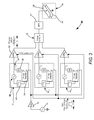
- FIG. 5 schematically illustrates an RFPS 90 in accordance with the present invention, wherein two arrangements 60 , here, designated 60 A and 60 B, have outputs thereof combined by a power combiner 18 .
- the combined output from the power combiner is transmitted via an impedance matching network (IMN) to discharge electrodes (not shown).
- INN impedance matching network
- Certain components of arrangement 60 are depicted at high level for convenience of illustration.
- Arrangements 60 A and 60 B are phase-locked to common reference oscillator 11 as discussed above.
- User pulse commands are delivered simultaneously to the RF switch S in each of arrangements 60 A and 60 B.
- 3 or more arrangements 60 can be combined in the same manner as the two arrangements depicted in FIG. 5 .
Landscapes
- Physics & Mathematics (AREA)
- Electromagnetism (AREA)
- Engineering & Computer Science (AREA)
- Plasma & Fusion (AREA)
- Optics & Photonics (AREA)
- Microelectronics & Electronic Packaging (AREA)
- Power Engineering (AREA)
- Lasers (AREA)
- Stabilization Of Oscillater, Synchronisation, Frequency Synthesizers (AREA)
Abstract
Description
Claims (15)
Priority Applications (2)
| Application Number | Priority Date | Filing Date | Title |
|---|---|---|---|
| US13/338,574 US8842704B2 (en) | 2011-12-28 | 2011-12-28 | Multiple phase-locked loops for high-power RF-power combiners |
| PCT/US2012/070737 WO2013101609A1 (en) | 2011-12-28 | 2012-12-19 | Multiple phase-locked loops for high-power rf-power combiners |
Applications Claiming Priority (1)
| Application Number | Priority Date | Filing Date | Title |
|---|---|---|---|
| US13/338,574 US8842704B2 (en) | 2011-12-28 | 2011-12-28 | Multiple phase-locked loops for high-power RF-power combiners |
Publications (2)
| Publication Number | Publication Date |
|---|---|
| US20130170512A1 US20130170512A1 (en) | 2013-07-04 |
| US8842704B2 true US8842704B2 (en) | 2014-09-23 |
Family
ID=47594998
Family Applications (1)
| Application Number | Title | Priority Date | Filing Date |
|---|---|---|---|
| US13/338,574 Active 2032-09-24 US8842704B2 (en) | 2011-12-28 | 2011-12-28 | Multiple phase-locked loops for high-power RF-power combiners |
Country Status (2)
| Country | Link |
|---|---|
| US (1) | US8842704B2 (en) |
| WO (1) | WO2013101609A1 (en) |
Cited By (3)
| Publication number | Priority date | Publication date | Assignee | Title |
|---|---|---|---|---|
| US20150287576A1 (en) * | 2012-12-18 | 2015-10-08 | Trumpf Huettinger Gmbh + Co. Kg | Extinguishing Arcs in a Plasma Chamber |
| US9276456B2 (en) | 2012-12-18 | 2016-03-01 | Trumpf Huettinger Gmbh + Co. Kg | Generating high-frequency power for a load |
| US20220199366A1 (en) * | 2018-09-28 | 2022-06-23 | Lam Research Corporation | Systems and methods for optimizing power delivery to an electrode of a plasma chamber |
Families Citing this family (6)
| Publication number | Priority date | Publication date | Assignee | Title |
|---|---|---|---|---|
| US9171843B2 (en) * | 2013-08-02 | 2015-10-27 | Taiwan Semiconductor Manufacturing Company, Ltd. | Semiconductor device and fabricating the same |
| JP6391706B2 (en) | 2013-12-24 | 2018-09-19 | オブシェストヴォ エス オグラニチェノイ オトヴェツトヴェノスティユ シーメンスOOO Siemens | Apparatus and method for RF high power generation |
| US9209964B2 (en) * | 2014-02-19 | 2015-12-08 | Cornet Technology, Inc. | Systems and methods for DTE/DCE CESoP timing |
| CN105846301B (en) * | 2016-06-04 | 2018-08-14 | 清华大学深圳研究生院 | A kind of high-power small size radio-frequency power supply |
| EP3758235B1 (en) * | 2019-06-25 | 2025-03-19 | Comet AG | Device and method for synchronizing a high frequency power signal and an external reference signal |
| EP3952113B1 (en) * | 2020-08-07 | 2026-04-08 | Comet AG | Control unit, radio frequency power generator, and method for generating synchronized radio frequency output signals |
Citations (13)
| Publication number | Priority date | Publication date | Assignee | Title |
|---|---|---|---|---|
| US4420723A (en) | 1980-04-01 | 1983-12-13 | U.S. Philips Corporation | Phase locked loop amplifier for variable amplitude radio waves |
| US4807232A (en) | 1987-12-28 | 1989-02-21 | United Technologies Corporation | Phase locked staggered dielectric ridge array waveguide gas laser |
| US5150372A (en) | 1991-09-13 | 1992-09-22 | Hughes Aircraft Company | Frequency sweeping phase-locked-loop synthesizer power supply for CO2 waveguide laser |
| US5625324A (en) | 1995-06-07 | 1997-04-29 | Hughes Electronics | Ultra low noise frequency generator producing the sum of plural signal sources |
| US5790942A (en) | 1995-05-31 | 1998-08-04 | Matra Communication | Frequency modulation radio transmission device |
| WO2000017969A1 (en) | 1998-09-21 | 2000-03-30 | Peter Vitruk | Truncated ridge waveguide for all-metal slab gas laser excitation |
| US20050186918A1 (en) | 2004-01-16 | 2005-08-25 | Stmicroelectronics Sa | RF integrated circuit comprising a frequency synthesizer not very sensitive to injection locking |
| US7157942B2 (en) * | 2004-12-08 | 2007-01-02 | Seiko Epson Corporation | Digital frequency difference detector with inherent low pass filtering and lock detection |
| US7372202B2 (en) | 2004-04-22 | 2008-05-13 | The Board Of Trustees Of The University Of Illinois | Phase locked microdischarge array and AC, RF or pulse excited microdischarge |
| US7579916B1 (en) | 2007-06-04 | 2009-08-25 | Rockwell Collins, Inc. | Low noise frequency synthesizer |
| US7755452B2 (en) | 2007-02-27 | 2010-07-13 | Coherent, Inc. | Power combiner |
| US20130051416A1 (en) * | 2011-08-23 | 2013-02-28 | Coherent, Inc. | Apparatus and method for balancing combined rf power- supplies for driving a co2 gas-discharge laser |
| US20130202004A1 (en) * | 2012-02-02 | 2013-08-08 | Coherent, Inc. | Output-power control apparatus for a co2 gas-discharge laser |
-
2011
- 2011-12-28 US US13/338,574 patent/US8842704B2/en active Active
-
2012
- 2012-12-19 WO PCT/US2012/070737 patent/WO2013101609A1/en not_active Ceased
Patent Citations (13)
| Publication number | Priority date | Publication date | Assignee | Title |
|---|---|---|---|---|
| US4420723A (en) | 1980-04-01 | 1983-12-13 | U.S. Philips Corporation | Phase locked loop amplifier for variable amplitude radio waves |
| US4807232A (en) | 1987-12-28 | 1989-02-21 | United Technologies Corporation | Phase locked staggered dielectric ridge array waveguide gas laser |
| US5150372A (en) | 1991-09-13 | 1992-09-22 | Hughes Aircraft Company | Frequency sweeping phase-locked-loop synthesizer power supply for CO2 waveguide laser |
| US5790942A (en) | 1995-05-31 | 1998-08-04 | Matra Communication | Frequency modulation radio transmission device |
| US5625324A (en) | 1995-06-07 | 1997-04-29 | Hughes Electronics | Ultra low noise frequency generator producing the sum of plural signal sources |
| WO2000017969A1 (en) | 1998-09-21 | 2000-03-30 | Peter Vitruk | Truncated ridge waveguide for all-metal slab gas laser excitation |
| US20050186918A1 (en) | 2004-01-16 | 2005-08-25 | Stmicroelectronics Sa | RF integrated circuit comprising a frequency synthesizer not very sensitive to injection locking |
| US7372202B2 (en) | 2004-04-22 | 2008-05-13 | The Board Of Trustees Of The University Of Illinois | Phase locked microdischarge array and AC, RF or pulse excited microdischarge |
| US7157942B2 (en) * | 2004-12-08 | 2007-01-02 | Seiko Epson Corporation | Digital frequency difference detector with inherent low pass filtering and lock detection |
| US7755452B2 (en) | 2007-02-27 | 2010-07-13 | Coherent, Inc. | Power combiner |
| US7579916B1 (en) | 2007-06-04 | 2009-08-25 | Rockwell Collins, Inc. | Low noise frequency synthesizer |
| US20130051416A1 (en) * | 2011-08-23 | 2013-02-28 | Coherent, Inc. | Apparatus and method for balancing combined rf power- supplies for driving a co2 gas-discharge laser |
| US20130202004A1 (en) * | 2012-02-02 | 2013-08-08 | Coherent, Inc. | Output-power control apparatus for a co2 gas-discharge laser |
Non-Patent Citations (6)
| Title |
|---|
| International Search Report and Written Opinion received for PCT Patent Application No. PCT/US2012/070737, mailed on May 10, 2013, 12 pages. |
| Razavi, Behzad, "RF Microelectronics: Chapter 8-Frequency Synthesizers", Prentice Hall Communications Engineering and Emerging Technologies Series, 1998, pp. 249-267. |
| Razavi, Behzad, "RF Microelectronics: Chapter 8-Frequency Synthesizers", Prentice Hall Communications Engineering and Emerging Technologies Series, 1998, pp. 285-289. |
| Razavi, Behzad, "RF Microelectronics: Chapter 8—Frequency Synthesizers", Prentice Hall Communications Engineering and Emerging Technologies Series, 1998, pp. 249-267. |
| Razavi, Behzad, "RF Microelectronics: Chapter 8—Frequency Synthesizers", Prentice Hall Communications Engineering and Emerging Technologies Series, 1998, pp. 285-289. |
| Schmelzer et al., U. S. Appl. No. 13/216,091, filed on Aug. 23, 2011, titled "Apparatus and Method for Balancing Combined RF Power Power Supplies for Driving A CO2 Gas-Discharge Laser", 22 pages. |
Cited By (9)
| Publication number | Priority date | Publication date | Assignee | Title |
|---|---|---|---|---|
| US20150287576A1 (en) * | 2012-12-18 | 2015-10-08 | Trumpf Huettinger Gmbh + Co. Kg | Extinguishing Arcs in a Plasma Chamber |
| US9276456B2 (en) | 2012-12-18 | 2016-03-01 | Trumpf Huettinger Gmbh + Co. Kg | Generating high-frequency power for a load |
| US10002749B2 (en) * | 2012-12-18 | 2018-06-19 | Trumpf Huettinger Gmbh + Co. Kg | Extinguishing arcs in a plasma chamber |
| US20180301323A1 (en) * | 2012-12-18 | 2018-10-18 | Trumpf Huettinger Gmbh + Co. Kg | Extinguishing Arcs in a Plasma Chamber |
| US10312064B2 (en) * | 2012-12-18 | 2019-06-04 | Trumpf Huettinger Gmbh + Co. Kg | Extinguishing arcs in a plasma chamber |
| US20220199366A1 (en) * | 2018-09-28 | 2022-06-23 | Lam Research Corporation | Systems and methods for optimizing power delivery to an electrode of a plasma chamber |
| US11908660B2 (en) * | 2018-09-28 | 2024-02-20 | Lam Research Corporation | Systems and methods for optimizing power delivery to an electrode of a plasma chamber |
| US20240186112A1 (en) * | 2018-09-28 | 2024-06-06 | Lam Research Corporation | Systems and methods for optimizing power delivery to an electrode of a plasma chamber |
| US12354840B2 (en) * | 2018-09-28 | 2025-07-08 | Lam Research Corporation | Systems and methods for optimizing power delivery to an electrode of a plasma chamber |
Also Published As
| Publication number | Publication date |
|---|---|
| WO2013101609A1 (en) | 2013-07-04 |
| US20130170512A1 (en) | 2013-07-04 |
Similar Documents
| Publication | Publication Date | Title |
|---|---|---|
| US8842704B2 (en) | Multiple phase-locked loops for high-power RF-power combiners | |
| EP2221850B1 (en) | Plasma power supply apparatus | |
| US7503996B2 (en) | Multiple frequency plasma chamber, switchable RF system, and processes using same | |
| KR100318788B1 (en) | Rf plasma power supply combining technique for increased stability | |
| US6920312B1 (en) | RF generating system with fast loop control | |
| US4665524A (en) | Mode locked laser light sources | |
| US6297704B1 (en) | Oscillation circuits featuring coaxial resonators | |
| US6181719B1 (en) | Gas laser RF power source apparatus and method | |
| CN105830195A (en) | Power supply system and method for generating power | |
| JP2016508281A (en) | Method for generating high frequency power and power supply system with power converter for supplying power to a load | |
| KR101927439B1 (en) | Apparatus of supplying power for generating plasma | |
| US4748634A (en) | Pumping system for RF excited gas devices | |
| US8654805B2 (en) | Apparatus and method for balancing combined RF power-supplies for driving a CO2 gas-discharge laser | |
| US4737737A (en) | Transmission injection-locked dielectric resonator oscillator | |
| GB2425415A (en) | Phase locking magnetrons | |
| US6693931B1 (en) | Method and system for phase stabilization | |
| US7538882B2 (en) | Systems and methods for assisting start of electrodeless RF discharge in a ring laser gyro | |
| Urbanski et al. | An Upgrade of Radio Frequency Reference Generation and Distribution Modules for FLASH2020 | |
| JPH11185999A (en) | High frequency pulse voltage generation method for accelerator and device thereof | |
| JP2007082171A (en) | Magnetron oscillation device | |
| US20110279165A1 (en) | Low Phase Noise RF Signal Generating System and Phase Noise Measurement Calibrating Method | |
| TW552771B (en) | Voltage control type oscillator and phase synchronized oscillator using the same | |
| US12010784B2 (en) | Wireless synchronization for multi-channel RF heating and drying devices | |
| Allen et al. | Design and Operation of the SPEAR II RF System | |
| Fong et al. | Commissioning of the TRIUMF ISAC RF system |
Legal Events
| Date | Code | Title | Description |
|---|---|---|---|
| AS | Assignment |
Owner name: COHERENT, INC., CALIFORNIA Free format text: ASSIGNMENT OF ASSIGNORS INTEREST;ASSIGNORS:SCHMELZER, DAVID P.;ROBOTHAM, W. SHEF, JR.;HAUER, FREDERICK W.;AND OTHERS;REEL/FRAME:027774/0126 Effective date: 20120104 |
|
| FEPP | Fee payment procedure |
Free format text: PAYOR NUMBER ASSIGNED (ORIGINAL EVENT CODE: ASPN); ENTITY STATUS OF PATENT OWNER: LARGE ENTITY |
|
| STCF | Information on status: patent grant |
Free format text: PATENTED CASE |
|
| AS | Assignment |
Owner name: BARCLAYS BANK PLC, AS COLLATERAL AGENT, NEW YORK Free format text: NOTICE OF GRANT OF SECURITY INTEREST IN PATENTS;ASSIGNOR:COHERENT, INC.;REEL/FRAME:040575/0001 Effective date: 20161107 |
|
| MAFP | Maintenance fee payment |
Free format text: PAYMENT OF MAINTENANCE FEE, 4TH YEAR, LARGE ENTITY (ORIGINAL EVENT CODE: M1551) Year of fee payment: 4 |
|
| MAFP | Maintenance fee payment |
Free format text: PAYMENT OF MAINTENANCE FEE, 8TH YEAR, LARGE ENTITY (ORIGINAL EVENT CODE: M1552); ENTITY STATUS OF PATENT OWNER: LARGE ENTITY Year of fee payment: 8 |
|
| AS | Assignment |
Owner name: JPMORGAN CHASE BANK, N.A., AS COLLATERAL AGENT, NEW YORK Free format text: SECURITY INTEREST;ASSIGNORS:II-VI INCORPORATED;II-VI DELAWARE, INC.;M CUBED TECHNOLOGIES, INC.;AND OTHERS;REEL/FRAME:060562/0254 Effective date: 20220701 Owner name: COHERENT, INC., CALIFORNIA Free format text: PATENT RELEASE AND REASSIGNMENT - RELEASE OF REEL/FRAME 040575/0001;ASSIGNOR:BARCLAYS BANK PLC, AS COLLATERAL AGENT;REEL/FRAME:060562/0650 Effective date: 20220701 |
|
| MAFP | Maintenance fee payment |
Free format text: PAYMENT OF MAINTENANCE FEE, 12TH YEAR, LARGE ENTITY (ORIGINAL EVENT CODE: M1553); ENTITY STATUS OF PATENT OWNER: LARGE ENTITY Year of fee payment: 12 |