US8835215B2 - Method for forming superior local conductivity in self-organized nanodots of transparent conductive film by femtosecond laser - Google Patents
Method for forming superior local conductivity in self-organized nanodots of transparent conductive film by femtosecond laser Download PDFInfo
- Publication number
- US8835215B2 US8835215B2 US13/563,715 US201213563715A US8835215B2 US 8835215 B2 US8835215 B2 US 8835215B2 US 201213563715 A US201213563715 A US 201213563715A US 8835215 B2 US8835215 B2 US 8835215B2
- Authority
- US
- United States
- Prior art keywords
- femtosecond laser
- transparent conductive
- conductive film
- nanodots
- organized
- Prior art date
- Legal status (The legal status is an assumption and is not a legal conclusion. Google has not performed a legal analysis and makes no representation as to the accuracy of the status listed.)
- Expired - Fee Related, expires
Links
Images


Classifications
-
- H—ELECTRICITY
- H10—SEMICONDUCTOR DEVICES; ELECTRIC SOLID-STATE DEVICES NOT OTHERWISE PROVIDED FOR
- H10H—INORGANIC LIGHT-EMITTING SEMICONDUCTOR DEVICES HAVING POTENTIAL BARRIERS
- H10H20/00—Individual inorganic light-emitting semiconductor devices having potential barriers, e.g. light-emitting diodes [LED]
- H10H20/80—Constructional details
- H10H20/83—Electrodes
- H10H20/832—Electrodes characterised by their material
- H10H20/833—Transparent materials
-
- B—PERFORMING OPERATIONS; TRANSPORTING
- B23—MACHINE TOOLS; METAL-WORKING NOT OTHERWISE PROVIDED FOR
- B23K—SOLDERING OR UNSOLDERING; WELDING; CLADDING OR PLATING BY SOLDERING OR WELDING; CUTTING BY APPLYING HEAT LOCALLY, e.g. FLAME CUTTING; WORKING BY LASER BEAM
- B23K26/00—Working by laser beam, e.g. welding, cutting or boring
- B23K26/02—Positioning or observing the workpiece, e.g. with respect to the point of impact; Aligning, aiming or focusing the laser beam
- B23K26/06—Shaping the laser beam, e.g. by masks or multi-focusing
- B23K26/062—Shaping the laser beam, e.g. by masks or multi-focusing by direct control of the laser beam
- B23K26/0622—Shaping the laser beam, e.g. by masks or multi-focusing by direct control of the laser beam by shaping pulses
- B23K26/0624—Shaping the laser beam, e.g. by masks or multi-focusing by direct control of the laser beam by shaping pulses using ultrashort pulses, i.e. pulses of 1 ns or less
-
- B—PERFORMING OPERATIONS; TRANSPORTING
- B82—NANOTECHNOLOGY
- B82Y—SPECIFIC USES OR APPLICATIONS OF NANOSTRUCTURES; MEASUREMENT OR ANALYSIS OF NANOSTRUCTURES; MANUFACTURE OR TREATMENT OF NANOSTRUCTURES
- B82Y30/00—Nanotechnology for materials or surface science, e.g. nanocomposites
-
- B—PERFORMING OPERATIONS; TRANSPORTING
- B82—NANOTECHNOLOGY
- B82Y—SPECIFIC USES OR APPLICATIONS OF NANOSTRUCTURES; MEASUREMENT OR ANALYSIS OF NANOSTRUCTURES; MANUFACTURE OR TREATMENT OF NANOSTRUCTURES
- B82Y40/00—Manufacture or treatment of nanostructures
-
- H01L33/42—
-
- H—ELECTRICITY
- H10—SEMICONDUCTOR DEVICES; ELECTRIC SOLID-STATE DEVICES NOT OTHERWISE PROVIDED FOR
- H10D—INORGANIC ELECTRIC SEMICONDUCTOR DEVICES
- H10D64/00—Electrodes of devices having potential barriers
- H10D64/01—Manufacture or treatment
-
- H—ELECTRICITY
- H10—SEMICONDUCTOR DEVICES; ELECTRIC SOLID-STATE DEVICES NOT OTHERWISE PROVIDED FOR
- H10P—GENERIC PROCESSES OR APPARATUS FOR THE MANUFACTURE OR TREATMENT OF DEVICES COVERED BY CLASS H10
- H10P34/00—Irradiation with electromagnetic or particle radiation of wafers, substrates or parts of devices
- H10P34/40—Irradiation with electromagnetic or particle radiation of wafers, substrates or parts of devices with high-energy radiation
- H10P34/42—Irradiation with electromagnetic or particle radiation of wafers, substrates or parts of devices with high-energy radiation with electromagnetic radiation, e.g. laser annealing
-
- Y—GENERAL TAGGING OF NEW TECHNOLOGICAL DEVELOPMENTS; GENERAL TAGGING OF CROSS-SECTIONAL TECHNOLOGIES SPANNING OVER SEVERAL SECTIONS OF THE IPC; TECHNICAL SUBJECTS COVERED BY FORMER USPC CROSS-REFERENCE ART COLLECTIONS [XRACs] AND DIGESTS
- Y10—TECHNICAL SUBJECTS COVERED BY FORMER USPC
- Y10S—TECHNICAL SUBJECTS COVERED BY FORMER USPC CROSS-REFERENCE ART COLLECTIONS [XRACs] AND DIGESTS
- Y10S977/00—Nanotechnology
- Y10S977/84—Manufacture, treatment, or detection of nanostructure
- Y10S977/888—Shaping or removal of materials, e.g. etching
- Y10S977/889—Shaping or removal of materials, e.g. etching by laser ablation
-
- Y—GENERAL TAGGING OF NEW TECHNOLOGICAL DEVELOPMENTS; GENERAL TAGGING OF CROSS-SECTIONAL TECHNOLOGIES SPANNING OVER SEVERAL SECTIONS OF THE IPC; TECHNICAL SUBJECTS COVERED BY FORMER USPC CROSS-REFERENCE ART COLLECTIONS [XRACs] AND DIGESTS
- Y10—TECHNICAL SUBJECTS COVERED BY FORMER USPC
- Y10S—TECHNICAL SUBJECTS COVERED BY FORMER USPC CROSS-REFERENCE ART COLLECTIONS [XRACs] AND DIGESTS
- Y10S977/00—Nanotechnology
- Y10S977/84—Manufacture, treatment, or detection of nanostructure
- Y10S977/901—Manufacture, treatment, or detection of nanostructure having step or means utilizing electromagnetic property, e.g. optical, x-ray, electron beamm
Definitions
- the present invention proposes a simple and rapid method for fabricating metallic self-organized nanodots on the surface of a transparent conductive oxide (TCO), so as to effectively increase the local conductivity of the TCO.
- TCO transparent conductive oxide
- ITO film is a kind of transparent conductive oxide (TCO) film and plays an important role in Flat Panel displays, such as organic electro-luminescence display (OLED), plasma display panel (PDP), liquid crystal display (LCD), and light emitting diode (LED) display.
- OLED organic electro-luminescence display
- PDP plasma display panel
- LCD liquid crystal display
- LED light emitting diode
- U.S. Pat. No. 5,163,220 proposes a superstring technique to deposit Ag and Ti films on an ITO film, wherein the Ag and Ti films are taken as metal bus bars for increasing the conductivity of the ITO film, so as to further increase the efficiency of the thin film electroluminescent (TFEL) display using the ITO film as the substrate thereof.
- TFEL thin film electroluminescent
- 7,687,349 forms metallic nanodots on the surface of a dielectric material (i.e., ITO film) by using two processes of: (1) reacting a silicon-containing gas precursor (e.g., silane) to form silicon nuclei over a dielectric film layer; and (2) using a metal precursor to form metallic nanodots where the metallic nanodots use the silicon nuclei from step (1) as nucleation points.
- a silicon-containing gas precursor e.g., silane
- femtosecond laser surface nanostructuring technique is recently applied in increasing the value added of some materials, such as metal, semiconductor and glass.
- some materials such as metal, semiconductor and glass.
- the femtosecond laser pulse is used and focused on a region with few microns size on the surface of a tungsten film, and then linear sub-wavelength periodic nanodots are fabricated and formed on the surface of the tungsten film.
- 25 p. 4462, 2003 proposes how to fabricate the similar sub-wavelength periodic nanodots on the surface of various compound semiconductors by using the femtosecond laser pulse.
- it focuses the single-beam femtosecond laser pulse to the surface of a glass for fabricating some periodic microstructures with the size of 1 ⁇ m ⁇ 1 ⁇ m and the spacing of 20 nm.
- U.S. Pat. No. 7,438,824 also utilizes and focuses the femtosecond laser pulse to the surface of a transparent or a translucent dielectric material for fabricating periodic microstructures with the assisting of a scanning platform.
- OPTICS EXPRESS paper of Vol. 18, No. 14, p. 14401, 2010 proposes the optical absorption of two dimensional periodic microstructures on ZnO crystal fabricated by the interference of two femtosecond laser beams.
- the femtosecond laser technique of this OPTICS EXPRESS paper also uses the scanning platform for carrying out the large area fabrication of the periodic microstructures on the surface of ZnO film.
- the person skilled in the related art can find that the conventional femtosecond laser techniques include the shortcomings and drawbacks as follows:
- Those conventional femtosecond laser techniques all utilize high fluences (0.1-0.4 J/cm 2 ) with a focused spot of hundred micrometers on the surface of semiconductor and dielectric materials, owing to the pulse broadening after an objective lens. However, this way still needs the assisting of a scanning platform in order to fabricate large size periodic microstructure on the surface of the dielectric material.
- the periodic microstructures made by using those conventional femtosecond laser techniques are all line patterns rather than nanodots array.
- the primary objective of the present invention is to provide a simple and rapid method, i.e., a method for forming superior local conductivity in self-organized nanodots on transparent conductive film induced by femtosecond laser pulse; in which the periodic ripple microstructures composed of self-organized nanodots can be directly fabricated on the surface of a transparent conductive oxide through the irradiation of the low-fluence femtosecond laser, without scanning; So that the method of the present invention includes the advantage of low equipment cost; moreover, to fabricate the metallic nanodots on the surface of the transparent conductive oxide is helpful to effectively increase the efficiency of OLED device and LED device.
- the inventors propose a method for forming superior local conductivity in self-organized nanodots on transparent conductive film induced by femtosecond laser pulse, comprising:
- a laser-emitting crystal emits a femtosecond laser pulse by a specific pulse number, wherein the femtosecond laser pulse has a specific pulse duration, a specific wavelength and a specific repetition rate;
- the off-axis parabolic mirror reflects the femtosecond laser pulses and maintains their pulse width in several ten fs at the position of sample. Then, the femtosecond laser pulses hit the surface of a transparent conductive film by a specific incident angle for fully exposing the surface of the transparent conductive film; (5) a constructive interference pattern is formed on the surface of the transparent conductive film by the femtosecond laser pulse, wherein the high energy of the constructive interference pattern is adequate to break a plurality of metal-oxygen bonds in the transparent conductive film, and then to form a plurality of metal-metal bonds; and (6) a plurality of periodic ripple microstructures composed of self-organized nanodots are formed on the surface of the transparent conductive film.
- FIG. 1 is a framework view of an emitting system of femtosecond laser pulse
- FIG. 2 is a flowchart of a method for forming superior local conductivity in self-organized nanodots on transparent conductive film induced by femtosecond laser pulses;
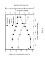
- FIG. 3 is curve plots of resistivity, carrier concentration and carrier mobility of an indium-tin-oxide film exposed by femtosecond laser pulses
- FIG. 4 is an SEM profile image, an AFM profile image and a surface current distribution image of the indium-tin-oxide film exposed by the femtosecond laser pulses;
- FIG. 5 is a schematic surface profile of the indium-tin-oxide film exposed by the femtosecond laser pulse
- FIG. 6 is an X-ray photoelectron energy spectrum of the indium-tin-oxide film.
- FIG. 7 is a schematic diagram of a surface model of the indium-tin-oxide film irradiated by the femtosecond laser pulse.
- FIG. 1 illustrates a framework view of the emitting system of femtosecond laser pulse.
- the emitting system 1 consists of a laser-emitting crystal 11 , an amplifier 12 and an off-axis parabolic mirror 13 , in which the laser-emitting crystal 11 is a titanium-doped sapphire laser crystal (Ti:sapphire).
- FIG. 2 there is shown a flowchart of the method for forming superior local conductivity in self-organized nanodots on transparent conductive film induced by femtosecond laser pulses. As shown in FIG. 1 and FIG.
- the specific pulse number is at least higher than 1000. (The reason for the specific pulse number must being higher than 1000 will be explained through experiment data in following descriptions.)
- step (S 02 ) for amplifying the femtosecond laser pulse by the amplifier 12 in order to make the femtosecond laser pulse include a specific pulse energy of 0.1 mJ/cm 2 .
- step (S 03 ) and step (S 04 ) in which the femtosecond laser pulse is facilitated to hit the surface of an off-axis parabolic mirror 13 and then reflected by the off-axis parabolic mirror 13 , such that the pulse width can be maintained in several ten fs at the position of sample.
- the laser beam was adjusted to ensure fully exposure for the parent conductive film 14 . As shown in FIG.
- step (S 04 ) the flow is next proceeded to step (S 05 ) for forming a constructive interference pattern on the surface of the transparent conductive film 14 by the femtosecond laser pulse, wherein the high energy of the constructive interference pattern is adequate to break a plurality of metal-oxygen bonds in the transparent conductive film 14 , and then to form a plurality of metal-metal bonds.
- step (S 06 ) is executed in the end of the flow, where a plurality of periodic ripple microstructures composed of self-organized nanodots being formed on the surface of the transparent conductive film 14 .
- the transparent conductive film 14 mentioned in above step (S 04 ) to step (S 06 ) is an indium-tin-oxide film including a plurality of In—O bonds and Sn—O bonds.
- the single-beam femtosecond laser pulse is used for breaking the In—O bonds and Sn—O bonds of the indium-tin-oxide film, so as to further form a plurality of In—In bonds in the surface of the indium-tin-oxide film, where the formed In—In bonds constitute the self-organized nanodots of the periodic ripple microstructures.
- the self-organized nanodots constituted by the In—In bonds have higher surface conductivity greater than the original surface conductivity of ITO film having In—O bonds and Sn—O bonds. Therefore, the surface current of those self-organized nanodots is of course higher than ITO film's.
- the resistivity, carrier concentration and carrier mobility of the indium-tin-oxide film exposed by the femtosecond laser pulse all change with the increase of the pulse number N, where N is a defined symbol rather than an element symbol.
- N is a defined symbol rather than an element symbol.
- the carrier mobility of the indium-tin-oxide film relatively descends from 12.3 cm 2 /V-s to 10.2 cm 2 /V-s
- the resistivity of the indium-tin-oxide film also relatively descends from 4.3 ⁇ 10 ⁇ 2 ⁇ -cm to 3.7 ⁇ 10 ⁇ 2 ⁇ -cm.
- FIG. 4 illustrates an SEM profile image, an AFM profile image and a surface current distribution image of the indium-tin-oxide film exposed by the femtosecond laser pulse, wherein the indium-tin-oxide film in FIG. 4( a ) is exposed by the femtosecond laser pulse with pulse energy of 0.1 mJ/cm 2 and pulse number N of 3 ⁇ 10 6 , and the SEM profile image of the indium-tin-oxide film in FIG. 4( a ) is captured by a scanning electron microscope (SEM).
- SEM scanning electron microscope
- the ripple spacings between the three periodic ripple microstructures can be determined to ⁇ 800 nm, ⁇ 400 nm and ⁇ 200 nm, respectively.
- the indium-tin-oxide film in FIG. 4( b ) is also exposed by the femtosecond laser pulse with pulse energy of 0.1 mJ/cm 2 and pulse number N of 3 ⁇ 10 6 , and the AFM profile image of the indium-tin-oxide film in FIG. 4( b ) is captured by a Atomic Force Microscopy (AFM).
- AFM Atomic Force Microscopy
- the indium-tin-oxide film in FIG. 4( c ) is also exposed by the femtosecond laser pulse with pulse energy of 0.1 mJ/cm 2 and pulse number N of 3 ⁇ 10 6 , and the surface current distribution image of the indium-tin-oxide film in FIG. 4( c ) is captured by a Current Sensing Atomic Force Microscopy (CSAFM).
- CSAFM Current Sensing Atomic Force Microscopy
- the high surface current distribution region in FIG. 4( c ) is extremely related to the nanodots forming region in FIG. 4( b ); it means that the nanodots forming region is high surface current distribution region.
- FIG. 6 there is shown an X-ray photoelectron energy spectrum of the indium-tin-oxide film, wherein the energy spectrum of FIG. 6 is measured by using an X-ray Photoelectron Spectrometer (XPS).
- XPS X-ray Photoelectron Spectrometer
- FIG. 7 illustrates a schematic diagram of the surface model of the indium-tin-oxide film.
- ITO film includes many In—O bonds and Sn—O bonds, and also includes some oxygen vacancies.
- Oxidide atoms There are three peaks of oxygen atoms (O1s) in XPS spectrum of FIG. 6 , which respectively represents the oxygen atoms bonded with metal atoms in ITO film (the peak is near to bonding energy of 529.6 ⁇ 0.1 eV), the oxygen atoms adjacent to oxygen vacancies in ITO film (the peak is near to bonding energy of 531 ⁇ 0.1 eV), and the oxygen atoms in hydroxyl (the peak is near to bonding energy of 532.6 ⁇ 0.1 eV.). Comparing FIG. 6( b ) with FIG.
- the value of the spectra energy peak of the oxygen atoms bonded with metal atoms in the ITO film exposed by the femtosecond laser pulse decreases with increasing pulse number N; it means that the In—O bonds and Sn—O bonds are broken and the oxygen atoms are released. So that, these released oxygen atoms bond with the metal atoms by hydroxyl type, for example, bonding with In atoms. Therefore, as in FIG. 6( d ), FIG. 6( e ), FIG. 6( f ), and FIG. 6( g ), the value of the spectra energy peak of the oxygen atoms in hydroxyl rises with increasing pulse number N.
- the experiment data proves that the ripple spacings of 800 nm and 400 nm are indeed accordant to the scattering model formula; however, the ripple spacing of 200 nm cannot accordant to the scattering model formula because the ripple spacing of 200 nm is largely small than the wavelength of the femtosecond laser pulse (800 nm).
- the ripple spacing of 200 nm is regarded as the SHG (second harmonic generation) result of 400 nm short wavelength on ITO film surface.
- the present invention has the following advantages:
- the method of the present invention merely uses single-beam femtosecond laser pulse to the surface of ITO film for fabricating periodic microstructures composed of self-organized nanodots, without depositing any metal films on the ITO film; And such method can increase 30 folds of surface current of the ITO film.
- the method of the present invention merely uses single-beam femtosecond laser pulse to the surface of ITO film for fabricating periodic microstructures composed of self-organized nanodots, without using any silicon-containing gas precursors; And such method can increase 30 folds of surface current of the ITO film.
- the periodic ripple microstructures composed of self-organized nanodots can be fabricated on the center surface of ITO chip with the size of 200 ⁇ m ⁇ 200 ⁇ m, without scanning. 4. Comparing to the conventional technique proposed by the paper published in international Journal of PHYSICAL REVIEW LETTERS , Vol. 91, No.
- the periodic ripple microstructures composed of self-organized nanodots can be fabricated on the center surface of ITO chip with the size of 200 ⁇ m ⁇ 200 ⁇ m, without scanning; And those periodic ripple microstructures include the ripple spacings of ⁇ 800 nm, ⁇ 400 nm and ⁇ 200 nm, respectively.
Landscapes
- Engineering & Computer Science (AREA)
- Physics & Mathematics (AREA)
- Optics & Photonics (AREA)
- Chemical & Material Sciences (AREA)
- Nanotechnology (AREA)
- Crystallography & Structural Chemistry (AREA)
- Condensed Matter Physics & Semiconductors (AREA)
- General Physics & Mathematics (AREA)
- Plasma & Fusion (AREA)
- Mechanical Engineering (AREA)
- Composite Materials (AREA)
- Materials Engineering (AREA)
- Manufacturing & Machinery (AREA)
- Laser Beam Processing (AREA)
Abstract
Description
2. The periodic microstructures made by using those conventional femtosecond laser techniques are all line patterns rather than nanodots array.
(5) a constructive interference pattern is formed on the surface of the transparent conductive film by the femtosecond laser pulse, wherein the high energy of the constructive interference pattern is adequate to break a plurality of metal-oxygen bonds in the transparent conductive film, and then to form a plurality of metal-metal bonds; and
(6) a plurality of periodic ripple microstructures composed of self-organized nanodots are formed on the surface of the transparent conductive film.
2. Comparing to the conventional technique of forming metallic nanodots on the surface of a dielectric material (i.e., ITO film) by using two processes proposed by U.S. Pat. No. 7,687,349, the method of the present invention merely uses single-beam femtosecond laser pulse to the surface of ITO film for fabricating periodic microstructures composed of self-organized nanodots, without using any silicon-containing gas precursors; And such method can increase 30 folds of surface current of the ITO film.
3. Comparing to the conventional technique proposed by OPTICS EXPRESS paper of Vol. 18, No. 14, p. 14401, 2010, the periodic ripple microstructures composed of self-organized nanodots can be fabricated on the center surface of ITO chip with the size of 200 μm×200 μm, without scanning.
4. Comparing to the conventional technique proposed by the paper published in international Journal of PHYSICAL REVIEW LETTERS, Vol. 91, No. 24, p. 247405-1, 2003, the periodic ripple microstructures composed of self-organized nanodots can be fabricated on the center surface of ITO chip with the size of 200 μm×200 μm, without scanning; And those periodic ripple microstructures include the ripple spacings of ˜800 nm, ˜400 nm and ˜200 nm, respectively.
Claims (10)
Applications Claiming Priority (2)
| Application Number | Priority Date | Filing Date | Title |
|---|---|---|---|
| TW101117069A TWI450313B (en) | 2012-05-14 | 2012-05-14 | Method for preparing self-assembled nano dot array on transparent conductive film surface by femtosecond laser pulse |
| TW101117069 | 2012-05-14 |
Publications (2)
| Publication Number | Publication Date |
|---|---|
| US20130299466A1 US20130299466A1 (en) | 2013-11-14 |
| US8835215B2 true US8835215B2 (en) | 2014-09-16 |
Family
ID=49547845
Family Applications (1)
| Application Number | Title | Priority Date | Filing Date |
|---|---|---|---|
| US13/563,715 Expired - Fee Related US8835215B2 (en) | 2012-05-14 | 2012-07-31 | Method for forming superior local conductivity in self-organized nanodots of transparent conductive film by femtosecond laser |
Country Status (2)
| Country | Link |
|---|---|
| US (1) | US8835215B2 (en) |
| TW (1) | TWI450313B (en) |
Families Citing this family (4)
| Publication number | Priority date | Publication date | Assignee | Title |
|---|---|---|---|---|
| US9425121B2 (en) | 2013-09-11 | 2016-08-23 | Taiwan Semiconductor Manufacturing Company, Ltd. | Integrated fan-out structure with guiding trenches in buffer layer |
| US9455211B2 (en) | 2013-09-11 | 2016-09-27 | Taiwan Semiconductor Manufacturing Company, Ltd. | Integrated fan-out structure with openings in buffer layer |
| US20180105455A1 (en) * | 2016-10-17 | 2018-04-19 | Corning Incorporated | Silica test probe and other such devices |
| CN109317856A (en) * | 2018-11-19 | 2019-02-12 | 东莞市云方金属制品有限公司 | A kind of tin bar convenient for taking and tearing protecting film |
Citations (8)
| Publication number | Priority date | Publication date | Assignee | Title |
|---|---|---|---|---|
| US5163220A (en) | 1991-10-09 | 1992-11-17 | The Unites States Of America As Represented By The Secretary Of The Army | Method of enhancing the electrical conductivity of indium-tin-oxide electrode stripes |
| US7006747B2 (en) * | 2003-01-17 | 2006-02-28 | 3M Innovative Properties Company | Optical devices incorporating photo reactive polymers |
| US7438824B2 (en) | 2005-03-25 | 2008-10-21 | National Research Council Of Canada | Fabrication of long range periodic nanostructures in transparent or semitransparent dielectrics |
| US7655544B2 (en) * | 2005-10-21 | 2010-02-02 | Utah State University | Self-assembled nanostructures |
| US7687349B2 (en) | 2006-10-30 | 2010-03-30 | Atmel Corporation | Growth of silicon nanodots having a metallic coating using gaseous precursors |
| US7838851B2 (en) * | 2006-07-18 | 2010-11-23 | Instrument Technology Research Center, National Applied Research Laboratories | Method and device for fabricating nano-structure with patterned particle beam |
| US8367462B2 (en) * | 2010-04-21 | 2013-02-05 | Georgia Tech Research Corporation | Large-scale fabrication of vertically aligned ZnO nanowire arrays |
| US20130182445A1 (en) * | 2010-11-24 | 2013-07-18 | Universite De Liege | Method of manufacturing an improved optical layer for a light emitting device with surface nano-micro texturation based on coherent electromagnetic radiation speckle lithography |
Family Cites Families (3)
| Publication number | Priority date | Publication date | Assignee | Title |
|---|---|---|---|---|
| EP1896805A4 (en) * | 2005-06-14 | 2010-03-31 | Steven M Ebstein | Applications of laser-processed substrate for molecular diagnostics |
| US8279901B2 (en) * | 2010-02-24 | 2012-10-02 | Alcon Lensx, Inc. | High power femtosecond laser with adjustable repetition rate and simplified structure |
| US8735030B2 (en) * | 2010-04-15 | 2014-05-27 | Carl Zeiss Smt Gmbh | Method and apparatus for modifying a substrate surface of a photolithographic mask |
-
2012
- 2012-05-14 TW TW101117069A patent/TWI450313B/en not_active IP Right Cessation
- 2012-07-31 US US13/563,715 patent/US8835215B2/en not_active Expired - Fee Related
Patent Citations (8)
| Publication number | Priority date | Publication date | Assignee | Title |
|---|---|---|---|---|
| US5163220A (en) | 1991-10-09 | 1992-11-17 | The Unites States Of America As Represented By The Secretary Of The Army | Method of enhancing the electrical conductivity of indium-tin-oxide electrode stripes |
| US7006747B2 (en) * | 2003-01-17 | 2006-02-28 | 3M Innovative Properties Company | Optical devices incorporating photo reactive polymers |
| US7438824B2 (en) | 2005-03-25 | 2008-10-21 | National Research Council Of Canada | Fabrication of long range periodic nanostructures in transparent or semitransparent dielectrics |
| US7655544B2 (en) * | 2005-10-21 | 2010-02-02 | Utah State University | Self-assembled nanostructures |
| US7838851B2 (en) * | 2006-07-18 | 2010-11-23 | Instrument Technology Research Center, National Applied Research Laboratories | Method and device for fabricating nano-structure with patterned particle beam |
| US7687349B2 (en) | 2006-10-30 | 2010-03-30 | Atmel Corporation | Growth of silicon nanodots having a metallic coating using gaseous precursors |
| US8367462B2 (en) * | 2010-04-21 | 2013-02-05 | Georgia Tech Research Corporation | Large-scale fabrication of vertically aligned ZnO nanowire arrays |
| US20130182445A1 (en) * | 2010-11-24 | 2013-07-18 | Universite De Liege | Method of manufacturing an improved optical layer for a light emitting device with surface nano-micro texturation based on coherent electromagnetic radiation speckle lithography |
Non-Patent Citations (4)
| Title |
|---|
| Borowiec, et al. "Subwavelength ripple formation on the surfaces of compound semiconductors irradiated with femtosecond laser pulses", Applied Physics Letters, vol. 82, No. 25, p. 4462-4464, Jun. 23, 2003. |
| Jia, et al. "Optical absorption of two dimensional periodic microstructures on ZnO crystal fabricated by the interference of two femtosecond laser beams", Optics Express paper of vol. 18, No. 14, p. 14401-14408, Jun. 21, 2010. |
| Shimotsuma, et al. "Self-Organized Nanogratings in Glass Irradiated by Ultrashort Light Pulses", International Journal of Physical Review Letters, vol. 91, No. 24, p. 247405-1:4, Dec. 2003. |
| Zhao, et al. "Formation of subwavelength periodic structures on tungsten induced by ultrashort laser pulses", International Journal of Optics Letters, vol. 32, No. 13, p. 1932-1934, Jul. 1, 2007. |
Also Published As
| Publication number | Publication date |
|---|---|
| US20130299466A1 (en) | 2013-11-14 |
| TWI450313B (en) | 2014-08-21 |
| TW201346979A (en) | 2013-11-16 |
Similar Documents
| Publication | Publication Date | Title |
|---|---|---|
| Afshinmanesh et al. | Transparent metallic fractal electrodes for semiconductor devices | |
| Van De Groep et al. | Transparent conducting silver nanowire networks | |
| Park et al. | Ultrafast laser ablation of indium tin oxide thin films for organic light-emitting diode application | |
| US8367434B2 (en) | Method for fabricating a nanostructured substrate for OLED and method for fabricating an OLED | |
| US8921841B2 (en) | Porous glass substrate for displays and method of manufacturing the same | |
| WO2014097943A1 (en) | Metal dot substrate and method for manufacturing metal dot substrate | |
| US8835215B2 (en) | Method for forming superior local conductivity in self-organized nanodots of transparent conductive film by femtosecond laser | |
| JP2009009861A (en) | Organic EL device and manufacturing method thereof | |
| Chen et al. | Laser-induced periodic structures for light extraction efficiency enhancement of GaN-based light emitting diodes | |
| Jiang et al. | Periodic transparent nanowires in ITO film fabricated via femtosecond laser direct writing | |
| US20230141768A1 (en) | Display panel having blind hole to accomodate signals exchanged with under-display component | |
| JP2023503702A (en) | Light emitting device including capping layer and method for manufacturing same | |
| Eckhardt et al. | Laser microstructured metal thin films as promising alternative for indium based transparent electrodes | |
| Wei et al. | Laser-induced optoelectronic tuning of perovskite nanocrystal films for multicolor pattern displays | |
| Sahin et al. | Nanostructuring of ITO thin films through femtosecond laser ablation | |
| Wang et al. | Superior local conductivity in self-organized nanodots on indium-tin-oxide films induced by femtosecond laser pulses | |
| Theuring et al. | Laser perforated ultrathin metal films for transparent electrode applications | |
| Farid et al. | Onset and evolution of laser induced periodic surface structures on indium tin oxide thin films for clean ablation using a repetitively pulsed picosecond laser at low fluence | |
| Qian et al. | Nanosecond laser nanopatterning of highly ordered nanodot arrays on silicon surface: breaking the monopoly of femtosecond lasers | |
| Scorticati et al. | Optical and electrical properties of SnO2 thin films after ultra-short pulsed laser annealing | |
| Huang et al. | Plasmonic Field-Guided Patterning of Hybrid Nanostructured Gratings for Their Plasmon-Mediated Optical Activities | |
| Rajendran et al. | Properties of indium tin oxide films grown on microtextured glass substrates | |
| Sassmannshausen et al. | Ultrashort pulse selective laser ablation of multi-layer thin film systems | |
| JP2015011760A (en) | LAMINATE FOR SEMICONDUCTOR LIGHT EMITTING DEVICE, ITS MANUFACTURING METHOD, AND SEMICONDUCTOR LIGHT EMITTING DEVICE | |
| JP2015088388A (en) | Organic el element, and image display apparatus and illumination apparatus including the same |
Legal Events
| Date | Code | Title | Description |
|---|---|---|---|
| AS | Assignment |
Owner name: NATIONAL TSING HUA UNIVERSITY (TAIWAN), TAIWAN Free format text: ASSIGNMENT OF ASSIGNORS INTEREST;ASSIGNORS:LEU, JIH-PERNG;LUO, CHIH-WEI;WANG, CHIH;AND OTHERS;SIGNING DATES FROM 20120713 TO 20120723;REEL/FRAME:028692/0821 |
|
| STCF | Information on status: patent grant |
Free format text: PATENTED CASE |
|
| MAFP | Maintenance fee payment |
Free format text: PAYMENT OF MAINTENANCE FEE, 4TH YR, SMALL ENTITY (ORIGINAL EVENT CODE: M2551) Year of fee payment: 4 |
|
| FEPP | Fee payment procedure |
Free format text: MAINTENANCE FEE REMINDER MAILED (ORIGINAL EVENT CODE: REM.); ENTITY STATUS OF PATENT OWNER: SMALL ENTITY |
|
| LAPS | Lapse for failure to pay maintenance fees |
Free format text: PATENT EXPIRED FOR FAILURE TO PAY MAINTENANCE FEES (ORIGINAL EVENT CODE: EXP.); ENTITY STATUS OF PATENT OWNER: SMALL ENTITY |
|
| STCH | Information on status: patent discontinuation |
Free format text: PATENT EXPIRED DUE TO NONPAYMENT OF MAINTENANCE FEES UNDER 37 CFR 1.362 |
|
| FP | Lapsed due to failure to pay maintenance fee |
Effective date: 20220916 |