US8830966B2 - Discontinuous transmission in a frame - Google Patents
Discontinuous transmission in a frame Download PDFInfo
- Publication number
- US8830966B2 US8830966B2 US13/187,640 US201113187640A US8830966B2 US 8830966 B2 US8830966 B2 US 8830966B2 US 201113187640 A US201113187640 A US 201113187640A US 8830966 B2 US8830966 B2 US 8830966B2
- Authority
- US
- United States
- Prior art keywords
- indicators
- frame
- entries
- database
- dtx
- Prior art date
- Legal status (The legal status is an assumption and is not a legal conclusion. Google has not performed a legal analysis and makes no representation as to the accuracy of the status listed.)
- Expired - Fee Related, expires
Links
Images


Classifications
-
- H—ELECTRICITY
- H04—ELECTRIC COMMUNICATION TECHNIQUE
- H04B—TRANSMISSION
- H04B7/00—Radio transmission systems, i.e. using radiation field
- H04B7/24—Radio transmission systems, i.e. using radiation field for communication between two or more posts
-
- H—ELECTRICITY
- H04—ELECTRIC COMMUNICATION TECHNIQUE
- H04W—WIRELESS COMMUNICATION NETWORKS
- H04W52/00—Power management, e.g. Transmission Power Control [TPC] or power classes
- H04W52/02—Power saving arrangements
- H04W52/0209—Power saving arrangements in terminal devices
- H04W52/0212—Power saving arrangements in terminal devices managed by the network, e.g. network or access point is leader and terminal is follower
- H04W52/0216—Power saving arrangements in terminal devices managed by the network, e.g. network or access point is leader and terminal is follower using a pre-established activity schedule, e.g. traffic indication frame
-
- Y—GENERAL TAGGING OF NEW TECHNOLOGICAL DEVELOPMENTS; GENERAL TAGGING OF CROSS-SECTIONAL TECHNOLOGIES SPANNING OVER SEVERAL SECTIONS OF THE IPC; TECHNICAL SUBJECTS COVERED BY FORMER USPC CROSS-REFERENCE ART COLLECTIONS [XRACs] AND DIGESTS
- Y02—TECHNOLOGIES OR APPLICATIONS FOR MITIGATION OR ADAPTATION AGAINST CLIMATE CHANGE
- Y02D—CLIMATE CHANGE MITIGATION TECHNOLOGIES IN INFORMATION AND COMMUNICATION TECHNOLOGIES [ICT], I.E. INFORMATION AND COMMUNICATION TECHNOLOGIES AIMING AT THE REDUCTION OF THEIR OWN ENERGY USE
- Y02D30/00—Reducing energy consumption in communication networks
- Y02D30/70—Reducing energy consumption in communication networks in wireless communication networks
Definitions
- the present invention relates to wireless communication generally and, more particularly, to a method and/or apparatus for implementing a discontinuous transmission in a frame.
- FIG. 1 a flow diagram of a conventional transport channel multiplexing process 20 is shown.
- the processes 20 is used to transmit a radio frame in a downlink of a 3rd Generation Partnership Project system.
- the system specifies binary data bits and indication bits for a discontinuous transmission (i.e., DTX) state.
- the indication bits with the DTX state are used to fill non-data portions of the radio frame.
- Insertion points of the DTX indication bits i.e., 1st Insertion of DTX Indication block and 2nd Insertion of DTX Indication block
- the system decides which modes are used during a connection.
- adding the DTX indication bits to the radio frame means switching from working with one-bit symbols to working with two-or-more-bit symbols. The larger symbols are used to distinguish the DTX indication bits from the data bits.
- Working with greater than one-bit symbols effects a processing power used by the transport channel. Where no DTX indication bits are present in a radio frame, all of the processing power can work on only data bits. Furthermore, the data bits can be saved in a packed way (i.e., eight data bits packed into a byte) and can be handled in parallel. Where the DTX indication bits are added to the radio frame, the data bits and the DTX indication bits are distinguished by representing each with multiple bits.
- the present invention concerns an apparatus having a database and a circuit.
- the database may be configured to store a plurality of entries.
- the circuit may be configured to (i) insert a plurality of indicators into a frame, (ii) generate the entries in the database and (iii) transmit the frame in response to the entries such that power is applied to an antenna corresponding to each of a plurality of data items in the frame and no power is applied to the antenna corresponding to each of the indicators in the frame.
- Each of the entries generally identifies a respective location in the frame. Each of the locations may begin a respective string comprising at least one of the indicators.
- the objects, features and advantages of the present invention include providing discontinuous transmission in a frame that may (i) reduce processing power, (ii) avoid switching data bits from single-bit representations to multi-bit representations, (iii) use don't-care values for discontinuous transmission indicators (iv) save locations of the discontinuous transmission indicators external to a frame and/or (v) implement single-bit discontinuous transmission indicators.
- FIG. 1 is a flow diagram of a conventional transport channel multiplexing process
- FIG. 2 is a diagram illustrating a communications system implemented in accordance with an example embodiment of the present invention
- FIG. 3 is a diagram illustrating example components that may be employed by a base station in processing a downlink signal of the system
- FIG. 4 is a block diagram illustrating an example processing unit that may be configured to implement channel coding in accordance with a preferred embodiment of the present invention
- FIG. 5 is a flow diagram of an example method for adjusting a database for an initial interleave in the fixed mode
- FIG. 6 is a flow diagram of an example method for adjusting the database for a subsequent interleave in the fixed mode
- FIG. 7 is a diagram of an example method for multiplexing three transport channels in the fixed mode
- FIG. 8 is a flow diagram of an example method for adjusting the database for the subsequent interleave in a flexible mode.
- FIG. 9 is a diagram of an example method for multiplexing the three transport channels in the flexible mode.
- the system 100 may implement a wireless communications system.
- the system 100 may implement a third generation cellular communication system compliant with the 3GPP Multiplexing and Channel Coding specification (3GPP TS 25.212, version 10.1.0, December 2010).
- the system 100 generally comprises at least one base station 102 and a number of mobile units (or devices) 104 .
- the base station 102 may transmit signals to the mobile units 104 via a downlink channel 106 .
- Each of the mobile units 104 may transmit signals to the base stations 102 via an uplink channel 108 .
- the system 100 may also be implemented with multiple base stations 102 .
- the base station(s) 102 may include a processing unit 110 .
- Each of the mobile units 104 may include a processing unit 120 .
- the processing units 110 and 120 may be configured to manage communications between the base station(s) 102 and the mobile units 104 .
- the processing unit 110 may be configured to perform a downlink process for multiplexing and channel coding in a frequency division duplex mode of operation.
- the processor 110 may implement hardware to perform the downlink processing in accordance with the present invention.
- the downlink processing in accordance with the present invention may be performed by software executed on the processing unit 110 .
- the software for performing the downlink processing in accordance with the present invention may be written to a Flash memory or other nonvolatile memory (e.g., programmable read-only memory (PROM), erasable programmable read-only memory (EPROM), electrically erasable programmable read-only memory (EEPROM), bubble memory, disk or disc media, etc.).
- volatile memory such as dynamic random access memory (e.g., DRAM) or static random access memory (e.g., SRAM), may be used.
- the software may be loaded from a nonvolatile storage medium at power-up.
- a channel 130 may be implemented, for example, as a wireless communications channel.
- the channel 130 may be implemented as a cellular communications channel of a wireless communications network (e.g., a 3GPP radio access network, a 3GPP LTE network, etc.).
- the base station 102 may include a framing block (or circuit) 140 and a database 142 .
- the framing circuit 140 may be implemented with the processor 110 of FIG. 2 .
- FIG. 4 a block diagram is shown illustrating an example processing unit 150 that may be configured to implement channel coding in accordance with a preferred embodiment of the present invention.
- the processing unit 110 of FIG. 2 may be implemented using the processing unit 150 .
- the processing unit 150 may include, but is not limited to, a block (or circuit) 152 , a block (or circuit) 154 , a block (or circuit) 156 , a block (or circuit) 158 , a block (or circuit) 160 and a block (or circuit) 162 .
- the circuits 152 - 162 may represent modules and/or blocks that may be implemented as hardware, software, a combination of hardware and software, or other implementations.
- the circuit 152 may be implemented, in an example, as an embedded processor (e.g., ARM, etc.).
- the circuit 154 may be implemented as a read-only memory (e.g., ROM).
- the circuit 156 may comprise random access memory (e.g., RAM).
- the circuit 158 may implement a digital signal processor (e.g., DSP).
- the circuit 160 may be implemented, in an example, as an analog/RF unit (e.g., a transceiver). In another example, the circuit 160 may implement a transmitter and a receiver that are separate.
- the circuit 162 may implement an antenna (e.g., a cellular antenna, etc.).
- the circuit 160 may be configured to transmit and receive information via the antenna 162 .
- the circuits 152 - 160 may be connected together using one or more busses.
- the circuit 154 may store computer executable instructions for controlling the circuit 152 and/or the circuit 158 in accordance with the teachings presented herein.
- discontinuous transmission indicators may be implemented in addition to binary data items (e.g., data bits or data symbols).
- the DTX indicators (or symbols) are generally used to fill unused portions of a radio frame with bits.
- the insertion points of the DTX indicators typically depends on whether fixed positions per a fixed mode and/or flexible positions per a flexible mode are used for one or more transport (or traffic) channels (e.g., TrCHs) in the radio frame. Insertion of the DTX indicators is generally described in the 3GPP technical specification 25.212, section 4.2 “General Coding/Multiplexing of TrCHs”, which is hereby incorporated by reference.
- a universal terrestrial radio access network (e.g., UTRAN) generally decides for each coded composite transport channel (e.g., CCTrCH) whether the fixed positions or the flexible positions are used during a connection.
- the DTX indication bits may indicate when the transmission should be turned off.
- the DTX indication bits are generally not transmitted on the antenna 162 .
- Some embodiments of the present invention may reduce a width of the DTX indication bits and the data items in way that may lower a processing power used in preparing the transport channels.
- Some embodiments may implement the TrCH without the insertion of the DTX indicators, thereby reducing the processing power and the switching from 1 bit to a byte or 2 bits.
- single-bit DTX indicators may be “inserted” at the 1st Insertion of DTX Indication block and/or the 2nd Insertion of DTX Indication block (see FIG. 1 ).
- the single-bit DTX indicators may have don't-care values (e.g., binary 0 or binary 1). Therefore, no actual insertion of the DTX indicators may be performed in some embodiments.
- a set of entries may be stored in the database 142 .
- several (e.g., 30) entries may be stored.
- the maximum number of entries is generally determined by a maximum of 6 transport channels per user and so a maximum of 6 DTX indicators insertions may exist.
- the entries may also enable the transport channel to keep the data items at one-bit wide.
- Each entry generally provides an indication about the location of a DTX indicator in the frame at the end of the transport channel processing.
- Each entry generally has multiple (e.g., 2) values.
- a start value (e.g., DB_StartIndex) may indicate where a respective string of one or more DTX indicators starts in the frame.
- a size value (DB_NumOfDTX) generally indicates a number of bits (e.g., number of one-bit DTX indicators) in a respective string.
- the entries may be calculated in different ways for the flexible mode and the fixed mode.
- the database 142 generally holds the locations (or places) where the DTX indicators start and where the DTX indicators end. Instead of inserting the multi-bit DTX symbols, the single-bit DTX indicators may be inserted as regular bits with a logical one value, or a logical zero value. Therefore, each data items may remain represented by a single bit. The data items may be interleaved with the DTX indicators by performing the whole transport channel flow, as shown in FIG. 1 . Thereafter, the resulting frame may be transferred to the transceiver 160 along with the entries from the database 142 that locate the DTX indicators.
- the entries in the database 142 for the fixed mode may be built as follows:
- TrCHDTX(kk) may denote the number of DTX indicators (indication bits) in the transport channel kk.
- DTX(kk) may denote the number of DTX indicators added in a radio frame of the transport channel kk.
- P1c1(j) may denote an original column position of the j-th permuted column, see the inter-column permutation patterns for an initial (e.g., 1st) interleave operation in Table II.
- P2(j) may denote an original column position of the j-th permuted column, see the inter-column permutation patterns for a subsequent (e.g., 2nd) interleave operation in Table III (3GPP 25.212, section 4.2.11, “2nd Interleaving”, Table 7).
- NumOfTrCHs may denote the number of transport channels in a single radio frame.
- mS may denote milliseconds.
- Each column generally represents a radio frame.
- Each column generally represents a radio frame.
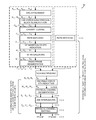
- the method (or process) 170 may be implemented by a combination of the circuit 140 and the database 142 .
- the method 170 generally comprises a step (or state) 172 , a step (or state) 174 , a step (or state) 176 , a step (or state) 178 , a step (or state) 180 , a step (or state) 182 , a step (or state) 184 , a step (or state) 186 , a step (or state) 188 , a step (or state) 190 and a step (or state) 192 .
- the steps 172 - 192 may represent modules and/or blocks that may be implemented as hardware, software, a combination of hardware and software, or other implementations.
- the transport channel information may be set to initial values.
- the number of transport channels (e.g., NumOfTrCHs) may be initialized to a predetermined value (e.g., 2).
- the values C1(1) and C1(2) may be initialized to predetermined values (e.g., 4 and 8).
- the pattern P1c1(1,:) may be set to a predetermined pattern (e.g., [0, 2, 1, 3]).
- the pattern P1c1(2,:) may be set to another predetermined pattern (e.g., [0, 4, 2, 6, 1, 5, 3, 7]).
- the circuit 140 may calculate a DTX column start value (e.g., DTXColumnStart) as a ceiling of X(kk)/C1(kk) for the transport channel kk.
- the circuit 140 may calculate a DTX row start value (e.g., DTXRowStart) as a modulo operation mod(X(kk),C1(kk)) in the step 176 .
- a modulo (or remainder) of DTX value e.g., ModOfDTX
- a number of interleaver rows value e.g., NumOfInterleaverRows
- database information of the number of DTX indicators in column ii of the transport channel kk (e.g., DB_NumOfDTXTrCH(kk,ii)) may be filled with the value NumOfInterleaverRows.
- the values DB_NumOfDTXTrCH in the database may be adjusted by the circuit 140 in the step 184 to account for the initial interleave.
- DB_NumOfDTXTrCH( kk,P 1 c 1( kk,ii+ DTXRowStart+1)+1) DB_NumOfDTXTrCH( kk,P 1 c 1( kk,ii+ DTXRowStart+1)+1)1, for each ii from 0 to ModOfDTX ⁇ 1.
- database information of the index of the start row of the DTX indicators in column ii of the transport channel kk may be filled with the value DTXColumnStart.
- the circuit 140 may check to see if more transport channels remain. If more transport channels are available, the circuit 140 may increment the current value kk up to the value NumOfTrCHs in the step 192 and continue with the step 174 . The loop around steps 174 to 192 may continue until all of the transport channels have been processed. Thereafter, the method 170 may end.
- the method 200 may be implemented by a combination of the circuit 140 and the database 142 .
- the method 200 generally comprises a step (or state) 202 , a step (or state) 204 , a step (or state) 206 , a step (or state) 208 , a step (or state) 210 , a step (or state) 212 , a step (or state) 214 , a step (or state) 216 , a step (or state) 218 , a step (or state) 220 , a step (or state) 222 , a step (or state) 224 , a step (or state) 226 and a step (or state) 228 .
- the steps 202 - 228 may represent modules and/or blocks that may be implemented as hardware, software, a combination of hardware and software, or other
- the circuit 140 may create a database for the subsequent interleave.
- a transport channel column index value (e.g., ColumnIndex(kk)) may be set to a predetermined value (e.g., 1).
- the number of bits in a radio frame of the transport channel kk (e.g., G(kk)) may be set to DB_StartIndexTrCH(kk,ColumnIndex(kk)) for each of the transport channels.
- the number of DTX indicators in a radio frame of the transport channel kk (e.g., DTX(kk)) may be set to DB_NumOfDTXTrCH(kk,ColumnIndex(kk)) for each of the transport channels.
- Different transport channels may have different transport channel column index values (e.g., ColumnIndex(kk)—where kk is the number of the transport channel).
- the circuit 140 may set the pattern P2 to a fixed pattern (e.g., [0, 20, 10, 5, 15, 25, 3, 13, 23, 8, 18, 28, 1, 11, 21, 6, 16, 26, 4, 14, 24, 19, 9, 29, 12, 2, 7, 22, 27, 17]).
- a data length value (e.g., DataLen) may be set to an initial value (e.g., 0) in the step 204 .
- the value DataLen may be updated by adding the value G(kk).
- the value DTXColumnStart may be calculated as a ceiling of DataLen/30 in the step 208 .
- the value DTXRowStart is generally calculated in the step 210 as a modulo operation mod(DataLen,30).
- the value DataLen may by updated by adding the value DTX(kk).
- the value ModOfDTX may be calculated in the step 214 as a modulo operation mod(DTX(kk),30).
- the value NumOfInterleaverRows may be calculated as a floor of DTX(kk)/30.
- the values DB_NumOfDTX(kk,P2(ii+1)+1) may be filled with the value NumOfInterleaverRows in the step 218 for each ii from 0 to 29 (e.g., a value for each of the 30 columns of the subsequent interleave).
- the values DB_NumOfDTX in the database may be adjusted to account for the subsequent interleave.
- DB_NumOfDTX( kk,P 2( ii+ DTXRowStart+1)+1) DB_NumOfDTX( kk,P 2( ii+ DTXRowStart+1)+1)+1, for ii from 0 to ModOfDTX ⁇ 1.
- the values DB_StartIndex(kk,P2(ii+1)+1) may be filled with the value DTXColumnStart for each ii from 0 to DTXRowStart ⁇ 1.
- the circuit 140 may check to see if more transport channels remain. If more transport channels are available, the circuit 140 may increment the transport channel value kk up to the value NumOfTrCHs in the step 228 and continue with the step 206 . The loop around steps 206 to 228 may continue until all of the transport channels have been processed. Thereafter, the method 200 may end.
- the method (or process) 240 may be implemented by a combination of the circuit 140 and the database 142 .
- the method 240 generally comprises a step (or state) 241 , a step (or state) 242 , a step (or state) 243 , a step (or state) 244 , a step (or state) 245 and a step (or state) 246 .
- the steps 241 - 246 may represent modules and/or blocks that may be implemented as hardware, software, a combination of hardware and software, or other implementations.
- the circuit 140 may perform a cyclic redundancy check attachment, transport block (TrBK) concatenation/code block segmentation, channel coding and rate matching in each of the transport channels in the step 241 .
- the first DTX indicator insertion may take place in each of the transport channels.
- the initial interleave within each transport channel may occur in the step 243 .
- the circuit 140 may perform the radio frame segmentation. Transport channel multiplexing of the individual transport channels into a single channel may be performed in the step 245 .
- the subsequent interleave may occur in the step 246 .
- each original set of DTX indicators may become a respective string of DTX indicators in the frame.
- the entries in the database 142 may point to the starting location and identify a length of a respective string.
- the entries in the database 142 for the flexible mode may be built as follows:
- P may denote the number of physical channels (e.g., PhCHs).
- R may denote the number of bits in a radio frame, including the data bits and the DTX indicators, for each PhCH.
- TotalDTX may denote the number of the total DTX indicators (bits).
- the method 250 may be implemented by a combination of the circuit 140 and the database 142 .
- the method 250 generally comprises a step (or state) 252 , a step (or state) 254 , a step (or state) 256 , a step (or state) 258 , a step (or state) 260 , a step (or state) 262 , a step (or state) 264 and a step (or state) 266 .
- the steps 252 - 266 may represent modules and/or blocks that may be implemented as hardware, software, a combination of hardware and software, or other implementations.
- the creation of the data base may be as follow.
- the pattern P2 may be set to an initial pattern (e.g., [0, 20, 10, 5, 15, 25, 3, 13, 23, 8, 18, 28, 1, 11, 21, 6, 16, 26, 4, 14, 24, 19, 9, 29, 12, 2, 7, 22, 27, 17]).
- the circuit 140 may calculate the value DTXColumnStart as a ceiling of S/30.
- the value DTXRowStart may be calculated in the step 254 as a modulo operation mod(S,30).
- the value ModOfDTX may be calculated as a modulo operation mod(TotalDTX,30) in the step 256 .
- the value NumOfInterleaverRows is generally calculated as a floor of TotalDTX/30.
- the values DB_NumOfDTX(P2(ii+1)+1) in the database may be filled with the value NumOfInterleaverRows in the step 260 for each ii from 0 to 29 (e.g., a value for each of the 30 columns of the subsequent interleave).
- the values DB_NumOfDTX may be adjusted by the circuit 140 to account for the subsequent interleave.
- the values DB_StartIndex(P2(ii+1)+1) may be filled with the value DTXColumnStart for ii from 0 to DTXRowStart ⁇ 1.
- the values DB_StartIndex may be adjusted by the circuit 140 to account for the subsequent interleave.
- the method (or process) 270 may be implemented by a combination of the circuit 140 and the database 142 .
- the method 270 generally comprises a step (or state) 272 , a step (or state) 274 , a step (or state) 276 , a step (or state) 278 , a step (or state) 280 and a step (or state) 282 .
- the steps 272 - 282 may represent modules and/or blocks that may be implemented as hardware, software, a combination of hardware and software, or other implementations.
- the circuit 140 may perform the cyclic redundancy check attachment, the transport block concatenation/code block segmentation, the channel coding and rate matching in each of the transport channels in the step 272 .
- the first DTX indicator insertion generally does not take place.
- the initial interleave within each transport channel may occur in the step 276 .
- the circuit 140 may perform the radio frame segmentation. Transport channel multiplexing of the individual transport channels into a single channel and the DTX insertion may be performed in the step 280 .
- the subsequent interleave may occur in the step 282 .
- the original set of DTX indicators may become a string of DTX indicators in the frame.
- the entries in the database 142 may point to the starting location and identify a length of the string.
- Implementations of some embodiments of the present invention may cause the initial interleave and the subsequent interleave to operate on one-bit data items instead of two-or-more-bit data items.
- the processing power used in processing the transport channels may be reduced compared with common approaches by having fewer bits to process.
- the DTX indicators may have don't-care values, no actual work may be performed during the DTX insertions. Whatever random values that happen to be in the frame at the DTX insertion locations may left in place.
- FIGS. 2-9 may be implemented using one or more of a conventional general purpose processor, digital computer, microprocessor, microcontroller, RISC (reduced instruction set computer) processor, CISC (complex instruction set computer) processor, SIMD (single instruction multiple data) processor, signal processor, central processing unit (CPU), arithmetic logic unit (ALU), video digital signal processor (VDSP) and/or similar computational machines, programmed according to the teachings of the present specification, as will be apparent to those skilled in the relevant art(s).
- RISC reduced instruction set computer
- CISC complex instruction set computer
- SIMD single instruction multiple data
- signal processor central processing unit
- CPU central processing unit
- ALU arithmetic logic unit
- VDSP video digital signal processor
- the present invention may also be implemented by the preparation of ASICs (application specific integrated circuits), Platform ASICs, FPGAs (field programmable gate arrays), PLDs (programmable logic devices), CPLDs (complex programmable logic device), sea-of-gates, RFICs (radio frequency integrated circuits), ASSPs (application specific standard products), monolithic integrated circuits, one or more chips or die arranged as flip-chip modules and/or multi-chip modules or by interconnecting an appropriate network of conventional component circuits, as is described herein, modifications of which will be readily apparent to those skilled in the art(s).
- ASICs application specific integrated circuits
- FPGAs field programmable gate arrays
- PLDs programmable logic devices
- CPLDs complex programmable logic device
- sea-of-gates RFICs (radio frequency integrated circuits)
- ASSPs application specific standard products
- monolithic integrated circuits one or more chips or die arranged as flip-chip modules and/or multi-chip modules or by
- the present invention thus may also include a computer product which may be a storage medium or media and/or a transmission medium or media including instructions which may be used to program a machine to perform one or more processes or methods in accordance with the present invention.
- a computer product which may be a storage medium or media and/or a transmission medium or media including instructions which may be used to program a machine to perform one or more processes or methods in accordance with the present invention.
- Execution of instructions contained in the computer product by the machine, along with operations of surrounding circuitry may transform input data into one or more files on the storage medium and/or one or more output signals representative of a physical object or substance, such as an audio and/or visual depiction.
- the storage medium may include, but is not limited to, any type of disk including floppy disk, hard drive, magnetic disk, optical disk, CD-ROM, DVD and magneto-optical disks and circuits such as ROMs (read-only memories), RAMS (random access memories), EPROMs (electronically programmable ROMs), EEPROMs (electronically erasable ROMs), UVPROM (ultra-violet erasable ROMs), Flash memory, magnetic cards, optical cards, and/or any type of media suitable for storing electronic instructions.
- ROMs read-only memories
- RAMS random access memories
- EPROMs electroly programmable ROMs
- EEPROMs electro-erasable ROMs
- UVPROM ultra-violet erasable ROMs
- Flash memory magnetic cards, optical cards, and/or any type of media suitable for storing electronic instructions.
- the elements of the invention may form part or all of one or more devices, units, components, systems, machines and/or apparatuses.
- the devices may include, but are not limited to, servers, workstations, storage array controllers, storage systems, personal computers, laptop computers, notebook computers, palm computers, personal digital assistants, portable electronic devices, battery powered devices, set-top boxes, encoders, decoders, transcoders, compressors, decompressors, pre-processors, post-processors, transmitters, receivers, transceivers, cipher circuits, cellular telephones, digital cameras, positioning and/or navigation systems, medical equipment, heads-up displays, wireless devices, audio recording, storage and/or playback devices, video recording, storage and/or playback devices, game platforms, peripherals and/or multi-chip modules.
- Those skilled in the relevant art(s) would understand that the elements of the invention may be implemented in other types of devices to meet the criteria of a particular application.
- the signals illustrated in FIGS. 2-4 represent logical data flows.
- the logical data flows are generally representative of physical data transferred between the respective blocks by, for example, address, data, and control signals and/or busses.
- the system represented by the system 100 may be implemented in hardware, software or a combination of hardware and software according to the teachings of the present disclosure, as would be apparent to those skilled in the relevant art(s).
- the term “simultaneously” is meant to describe events that share some common time period but the term is not meant to be limited to events that begin at the same point in time, end at the same point in time, or have the same duration.
Landscapes
- Engineering & Computer Science (AREA)
- Computer Networks & Wireless Communication (AREA)
- Signal Processing (AREA)
- Mobile Radio Communication Systems (AREA)
- Detection And Prevention Of Errors In Transmission (AREA)
Abstract
Description
| TABLE I | |||
| Bits | Symbols with DTX | ||
| 0 | 00 | ||
| 1 | 01 | ||
| |
10 | ||
| TABLE II | ||
| Number of | Inter-column permutation patterns | |
| TTI | columns C1 | <P1c1(0), P11c(1), . . . , P1c1(C1-1)> |
| 10 |
1 | <0> |
| 20 |
2 | <0, 1> |
| 40 mS | 4 | <0, 2, 1, 3> |
| 80 mS | 8 | <0, 4, 2, 6, 1, 5, 3, 7> |
| TABLE III | |
| Number of | Inter-column permutation patterns |
| columns C2 | <P2(0), P2(1), . . . , P2(C2-1)> |
| 30 | <0, 20, 10, 5, 15, 25, 3, 13, 23, 8, 18, 28, 1, 11, 21, |
| 6, 16, 26, 4, 14, 24, 19, 9, 29, 12, 2, 7, 22, 27, 17> | |
DB_NumOfDTXTrCH(kk,P1c1(kk,ii+DTXRowStart+1)+1)=DB_NumOfDTXTrCH(kk,P1c1(kk,ii+DTXRowStart+1)+1)1, for each ii from 0 to
DB_StartIndexTrCH(kk,P1c1(kk,ii+1)+1)=DTXColumnStart−1, for ii from 0 to
DB_NumOfDTX(kk,P2(ii+DTXRowStart+1)+1)=DB_NumOfDTX(kk,P2(ii+DTXRowStart+1)+1)+1, for ii from 0 to
DB_StartIndex(kk,P2(ii+1)+1)=DTXColumnStart, for ii from DTXRowStart to 29. (4)
TotalDTX=(P×R)−S. (5)
The pattern P2 may be set to an initial pattern (e.g., [0, 20, 10, 5, 15, 25, 3, 13, 23, 8, 18, 28, 1, 11, 21, 6, 16, 26, 4, 14, 24, 19, 9, 29, 12, 2, 7, 22, 27, 17]). In the
DB_NumOfDTX(P2(ii+DTXRowStart+1)+1)=DB_NumOfDTX(P2(ii+DTXRowStart+1)+1)+1, for ii from 0 to
In the
DB_StartIndex(P2(ii+1)+1)=DTXColumnStart−1, for ii from DTXRowStart to 29. (7)
Claims (18)
Priority Applications (1)
| Application Number | Priority Date | Filing Date | Title |
|---|---|---|---|
| US13/187,640 US8830966B2 (en) | 2011-07-21 | 2011-07-21 | Discontinuous transmission in a frame |
Applications Claiming Priority (1)
| Application Number | Priority Date | Filing Date | Title |
|---|---|---|---|
| US13/187,640 US8830966B2 (en) | 2011-07-21 | 2011-07-21 | Discontinuous transmission in a frame |
Publications (2)
| Publication Number | Publication Date |
|---|---|
| US20130022027A1 US20130022027A1 (en) | 2013-01-24 |
| US8830966B2 true US8830966B2 (en) | 2014-09-09 |
Family
ID=47555700
Family Applications (1)
| Application Number | Title | Priority Date | Filing Date |
|---|---|---|---|
| US13/187,640 Expired - Fee Related US8830966B2 (en) | 2011-07-21 | 2011-07-21 | Discontinuous transmission in a frame |
Country Status (1)
| Country | Link |
|---|---|
| US (1) | US8830966B2 (en) |
Citations (13)
| Publication number | Priority date | Publication date | Assignee | Title |
|---|---|---|---|---|
| US5953666A (en) | 1994-11-21 | 1999-09-14 | Nokia Telecommunications Oy | Digital mobile communication system |
| US6542538B2 (en) | 2000-01-10 | 2003-04-01 | Qualcomm Incorporated | Method and apparatus for testing wireless communication channels |
| US6556550B1 (en) | 1996-10-18 | 2003-04-29 | Nokia Telecommunications Oy | Method and equipment for transmitting terminal interface user data and status information |
| US20030086381A1 (en) * | 2001-10-19 | 2003-05-08 | Terry Stephen E. | System for improved power savings during full DTX mode of operation in the downlink |
| US6868075B1 (en) | 1999-09-28 | 2005-03-15 | Telefonaktiebolaget Lm Ericsson (Publ) | Method and apparatus for compressed mode communications over a radio interface |
| US7050439B1 (en) | 1997-12-31 | 2006-05-23 | Nokia Networks Oy | Method for performing discontinuous transmission in an asynchronous transfer mode |
| US20070280171A1 (en) * | 2006-05-31 | 2007-12-06 | Rafael Carmon | Method and apparatus for blind transport format detection using discontinuous transmission (DTX) detection |
| US7352722B2 (en) | 2002-05-13 | 2008-04-01 | Qualcomm Incorporated | Mitigation of link imbalance in a wireless communication system |
| US20080151854A1 (en) * | 2001-07-27 | 2008-06-26 | Soma Networks, Inc. | Method, system, and apparatus for transmitting interleaved data between stations |
| US20090310540A1 (en) * | 2000-04-03 | 2009-12-17 | Barany Peter A | Interleaving data over frames communicated in a wireless channel |
| US20100260121A1 (en) * | 2009-03-16 | 2010-10-14 | Qualcomm Incorporated | Discontinuous Uplink Transmission Operation and Interference Avoidance For a Multi-Carrier System |
| US20120082192A1 (en) * | 2010-10-01 | 2012-04-05 | Interdigital Patent Holdings, Inc. | Method and apparatus for transmitting pilot on multiple antennas |
| US20130225227A1 (en) * | 2010-11-04 | 2013-08-29 | Telefonakiebolaget Lm Ericsson (Publ) | Method and arrangement for power sharing in a base station |
-
2011
- 2011-07-21 US US13/187,640 patent/US8830966B2/en not_active Expired - Fee Related
Patent Citations (13)
| Publication number | Priority date | Publication date | Assignee | Title |
|---|---|---|---|---|
| US5953666A (en) | 1994-11-21 | 1999-09-14 | Nokia Telecommunications Oy | Digital mobile communication system |
| US6556550B1 (en) | 1996-10-18 | 2003-04-29 | Nokia Telecommunications Oy | Method and equipment for transmitting terminal interface user data and status information |
| US7050439B1 (en) | 1997-12-31 | 2006-05-23 | Nokia Networks Oy | Method for performing discontinuous transmission in an asynchronous transfer mode |
| US6868075B1 (en) | 1999-09-28 | 2005-03-15 | Telefonaktiebolaget Lm Ericsson (Publ) | Method and apparatus for compressed mode communications over a radio interface |
| US6542538B2 (en) | 2000-01-10 | 2003-04-01 | Qualcomm Incorporated | Method and apparatus for testing wireless communication channels |
| US20090310540A1 (en) * | 2000-04-03 | 2009-12-17 | Barany Peter A | Interleaving data over frames communicated in a wireless channel |
| US20080151854A1 (en) * | 2001-07-27 | 2008-06-26 | Soma Networks, Inc. | Method, system, and apparatus for transmitting interleaved data between stations |
| US20030086381A1 (en) * | 2001-10-19 | 2003-05-08 | Terry Stephen E. | System for improved power savings during full DTX mode of operation in the downlink |
| US7352722B2 (en) | 2002-05-13 | 2008-04-01 | Qualcomm Incorporated | Mitigation of link imbalance in a wireless communication system |
| US20070280171A1 (en) * | 2006-05-31 | 2007-12-06 | Rafael Carmon | Method and apparatus for blind transport format detection using discontinuous transmission (DTX) detection |
| US20100260121A1 (en) * | 2009-03-16 | 2010-10-14 | Qualcomm Incorporated | Discontinuous Uplink Transmission Operation and Interference Avoidance For a Multi-Carrier System |
| US20120082192A1 (en) * | 2010-10-01 | 2012-04-05 | Interdigital Patent Holdings, Inc. | Method and apparatus for transmitting pilot on multiple antennas |
| US20130225227A1 (en) * | 2010-11-04 | 2013-08-29 | Telefonakiebolaget Lm Ericsson (Publ) | Method and arrangement for power sharing in a base station |
Non-Patent Citations (1)
| Title |
|---|
| 3GPP TS 25.212, "3rd Generation Partnership Project;Technical Specification Group Radio Access Network; Multiplexing and channel coding (FDD)", (Release 10), V10.1.0, (Dec. 2010). * |
Also Published As
| Publication number | Publication date |
|---|---|
| US20130022027A1 (en) | 2013-01-24 |
Similar Documents
| Publication | Publication Date | Title |
|---|---|---|
| EP4258786B1 (en) | Pusch scheduling transmission methods, terminal and network side device | |
| EP3716509B1 (en) | Encoding method and apparatus, electronic device and storage medium | |
| CN109075799B (en) | Encoding and decoding methods and devices of polar codes | |
| EP1656737B1 (en) | Method and apparatus for varying lengths of low density parity check codewords | |
| WO2021103978A1 (en) | Polar code encoding method, and device | |
| US8261175B2 (en) | Method and apparatus for performing a CRC check | |
| US20200067531A1 (en) | Polar code encoding and decoding method and apparatus | |
| US9819445B1 (en) | Method and apparatus for joint rate matching and deinterleaving | |
| CN102739600A (en) | Method for reducing latency on lte dl implementation | |
| KR20090031783A (en) | Symbol rate hardware accelerator | |
| US7515579B2 (en) | Dynamic switching of a transmission time interval in a wireless system | |
| CN112703687B (en) | Channel coding method and device | |
| EP3654557A1 (en) | Code block segmentation method, terminal, base station, and computer-readable storage medium | |
| US8879671B2 (en) | Worker and iteration control for parallel turbo decoder | |
| JP5440887B2 (en) | Control channel encoder for block coding with variable rate block code and method of operation thereof | |
| WO2021040681A1 (en) | Activation/release operation for sps and cg type 2 with a dci having configurable dci field sizes | |
| US10805045B2 (en) | Polar code encoding method and device and polar code decoding method and device | |
| US9385804B2 (en) | Transmission unit and a method for transmitting data | |
| TWI768035B (en) | Distributed crc polar codes | |
| US8830966B2 (en) | Discontinuous transmission in a frame | |
| US20190363827A1 (en) | Data processing method and communications device | |
| JP3920220B2 (en) | Communication device | |
| US11277154B2 (en) | Polar code-based interleaving method and communication apparatus | |
| US7269149B2 (en) | Interleaving for mobile communications | |
| CN110785937B (en) | CRC and polarization code transmission scheme |
Legal Events
| Date | Code | Title | Description |
|---|---|---|---|
| AS | Assignment |
Owner name: LSI CORPORATION, CALIFORNIA Free format text: ASSIGNMENT OF ASSIGNORS INTEREST;ASSIGNORS:KALFON, SHAI;GAZIT, IDO;REEL/FRAME:026626/0968 Effective date: 20110721 |
|
| AS | Assignment |
Owner name: DEUTSCHE BANK AG NEW YORK BRANCH, AS COLLATERAL AG Free format text: PATENT SECURITY AGREEMENT;ASSIGNORS:LSI CORPORATION;AGERE SYSTEMS LLC;REEL/FRAME:032856/0031 Effective date: 20140506 Owner name: DEUTSCHE BANK AG NEW YORK BRANCH, AS COLLATERAL AGENT, NEW YORK Free format text: PATENT SECURITY AGREEMENT;ASSIGNORS:LSI CORPORATION;AGERE SYSTEMS LLC;REEL/FRAME:032856/0031 Effective date: 20140506 |
|
| AS | Assignment |
Owner name: AVAGO TECHNOLOGIES GENERAL IP (SINGAPORE) PTE. LTD Free format text: ASSIGNMENT OF ASSIGNORS INTEREST;ASSIGNOR:LSI CORPORATION;REEL/FRAME:035390/0388 Effective date: 20140814 |
|
| AS | Assignment |
Owner name: AGERE SYSTEMS LLC, PENNSYLVANIA Free format text: TERMINATION AND RELEASE OF SECURITY INTEREST IN PATENT RIGHTS (RELEASES RF 032856-0031);ASSIGNOR:DEUTSCHE BANK AG NEW YORK BRANCH, AS COLLATERAL AGENT;REEL/FRAME:037684/0039 Effective date: 20160201 Owner name: LSI CORPORATION, CALIFORNIA Free format text: TERMINATION AND RELEASE OF SECURITY INTEREST IN PATENT RIGHTS (RELEASES RF 032856-0031);ASSIGNOR:DEUTSCHE BANK AG NEW YORK BRANCH, AS COLLATERAL AGENT;REEL/FRAME:037684/0039 Effective date: 20160201 |
|
| FEPP | Fee payment procedure |
Free format text: MAINTENANCE FEE REMINDER MAILED (ORIGINAL EVENT CODE: REM.) |
|
| LAPS | Lapse for failure to pay maintenance fees |
Free format text: PATENT EXPIRED FOR FAILURE TO PAY MAINTENANCE FEES (ORIGINAL EVENT CODE: EXP.); ENTITY STATUS OF PATENT OWNER: LARGE ENTITY |
|
| STCH | Information on status: patent discontinuation |
Free format text: PATENT EXPIRED DUE TO NONPAYMENT OF MAINTENANCE FEES UNDER 37 CFR 1.362 |
|
| FP | Lapsed due to failure to pay maintenance fee |
Effective date: 20180909 |