US8823904B2 - Liquid crystal display device - Google Patents
Liquid crystal display device Download PDFInfo
- Publication number
- US8823904B2 US8823904B2 US12/981,068 US98106810A US8823904B2 US 8823904 B2 US8823904 B2 US 8823904B2 US 98106810 A US98106810 A US 98106810A US 8823904 B2 US8823904 B2 US 8823904B2
- Authority
- US
- United States
- Prior art keywords
- alignment
- substrate
- display area
- molecules
- disposed
- Prior art date
- Legal status (The legal status is an assumption and is not a legal conclusion. Google has not performed a legal analysis and makes no representation as to the accuracy of the status listed.)
- Active, expires
Links
Images


Classifications
-
- G—PHYSICS
- G02—OPTICS
- G02F—OPTICAL DEVICES OR ARRANGEMENTS FOR THE CONTROL OF LIGHT BY MODIFICATION OF THE OPTICAL PROPERTIES OF THE MEDIA OF THE ELEMENTS INVOLVED THEREIN; NON-LINEAR OPTICS; FREQUENCY-CHANGING OF LIGHT; OPTICAL LOGIC ELEMENTS; OPTICAL ANALOGUE/DIGITAL CONVERTERS
- G02F1/00—Devices or arrangements for the control of the intensity, colour, phase, polarisation or direction of light arriving from an independent light source, e.g. switching, gating or modulating; Non-linear optics
- G02F1/01—Devices or arrangements for the control of the intensity, colour, phase, polarisation or direction of light arriving from an independent light source, e.g. switching, gating or modulating; Non-linear optics for the control of the intensity, phase, polarisation or colour
- G02F1/13—Devices or arrangements for the control of the intensity, colour, phase, polarisation or direction of light arriving from an independent light source, e.g. switching, gating or modulating; Non-linear optics for the control of the intensity, phase, polarisation or colour based on liquid crystals, e.g. single liquid crystal display cells
- G02F1/133—Constructional arrangements; Operation of liquid crystal cells; Circuit arrangements
- G02F1/1333—Constructional arrangements; Manufacturing methods
- G02F1/1337—Surface-induced orientation of the liquid crystal molecules, e.g. by alignment layers
- G02F1/133753—Surface-induced orientation of the liquid crystal molecules, e.g. by alignment layers with different alignment orientations or pretilt angles on a same surface, e.g. for grey scale or improved viewing angle
-
- G—PHYSICS
- G02—OPTICS
- G02F—OPTICAL DEVICES OR ARRANGEMENTS FOR THE CONTROL OF LIGHT BY MODIFICATION OF THE OPTICAL PROPERTIES OF THE MEDIA OF THE ELEMENTS INVOLVED THEREIN; NON-LINEAR OPTICS; FREQUENCY-CHANGING OF LIGHT; OPTICAL LOGIC ELEMENTS; OPTICAL ANALOGUE/DIGITAL CONVERTERS
- G02F1/00—Devices or arrangements for the control of the intensity, colour, phase, polarisation or direction of light arriving from an independent light source, e.g. switching, gating or modulating; Non-linear optics
- G02F1/01—Devices or arrangements for the control of the intensity, colour, phase, polarisation or direction of light arriving from an independent light source, e.g. switching, gating or modulating; Non-linear optics for the control of the intensity, phase, polarisation or colour
- G02F1/13—Devices or arrangements for the control of the intensity, colour, phase, polarisation or direction of light arriving from an independent light source, e.g. switching, gating or modulating; Non-linear optics for the control of the intensity, phase, polarisation or colour based on liquid crystals, e.g. single liquid crystal display cells
- G02F1/137—Devices or arrangements for the control of the intensity, colour, phase, polarisation or direction of light arriving from an independent light source, e.g. switching, gating or modulating; Non-linear optics for the control of the intensity, phase, polarisation or colour based on liquid crystals, e.g. single liquid crystal display cells characterised by the electro-optical or magneto-optical effect, e.g. field-induced phase transition, orientation effect, guest-host interaction or dynamic scattering
- G02F1/13718—Devices or arrangements for the control of the intensity, colour, phase, polarisation or direction of light arriving from an independent light source, e.g. switching, gating or modulating; Non-linear optics for the control of the intensity, phase, polarisation or colour based on liquid crystals, e.g. single liquid crystal display cells characterised by the electro-optical or magneto-optical effect, e.g. field-induced phase transition, orientation effect, guest-host interaction or dynamic scattering based on a change of the texture state of a cholesteric liquid crystal
Definitions
- the present invention is related to a liquid crystal display (LCD) device, particularly to an improved type of LCD device with wide-viewing-angle and high optical transmittance.
- LCD liquid crystal display
- the intensity of light passing through a LCD device is controlled by the alignments of liquid crystal (LC) molecules between two transparent electrodes of the device.
- LC liquid crystal
- the optical transmittance and the viewing angle can be very distinct for different types of LCD devices.
- the device can exhibit a superior optical transmittance.
- the problem of TN type LCD is that viewing angles are very restrictive.
- MVA multi-domain vertical alignment
- PVA patterned vertical alignment
- ITO protrusions or electrode
- LC liquid crystal
- the LC device of the present invention uses TN type LC with chiral dopants, such that the LC molecules within the display area can form a continuous-domain or multi-domain alignments, similar to the MVA or PVA modes.
- the present invention not only improves the viewing angle of LC devices, but also takes the advantage of high transmittance in conventional TN type LC.
- FIG. 1 is a top view of the LC alignments in a square display area.
- FIG. 2 is a cross sectional views of LC molecules in the twisted vertical alignment mode under a high gray-level driving voltage.
- FIG. 3 is a schematic illustrating the definition of ⁇ angle.
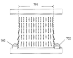
- FIG. 7 is a schematic illustrating the structure of protrusions disposing at edges of a display area for LC alignments.
- FIGS. 8C and 8D are the measured transmittance patterns of a TVA mode LC under a low gray-level ( 8 C) and a high gray-level ( 8 D) driving voltages.
- FIG. 10 shows a series of extended structures for LC alignment according to the first LC alignment structure of the present invention.
- FIG. 11 is a schematic illustrating the second LC alignment structures being disposed at the geometric center of the display area of the present invention.
- FIG. 12 is a schematic illustrating the structure electrode patterns of the lower substrate under the display area of the present invention.
- FIGS. 13A and 13B are the top view of the middle LC layer and the corresponding transmittance map using the TVA mode LC of the present invention.
- FIG. 14 shows a series of extended structures for LC alignment according to the structure of multi-domain alignment of the present invention.
- FIG. 15 shows a series of structures for surface alignment used in the present invention.
- the main feature of the present invention is the symmetric design of the LC alignment apparatus in the display area, in which TN type LC with chiral dopants will form a continuous-domain or multi-domain alignments.
- a pixel generally consists of at least one display area, of which the geometric shape can be, but not limited to, a square or a rectangular.
- FIG. 1 is a top view of the LC alignment of the present invention and shows a square display area 101 .
- the alignment of LC molecules 102 twisted gradually from the first substrate to the second substrate, forming a symmetrically radial alignment. Because the long axes of the LC molecules are aligned along all azimuthal angles, a wide viewing angle can be achieved. In addition, due to the twisted alignment of the LC molecules, no singular point will occur. Therefore, by optimizing the phase and twisting angle of the LC molecules, a higher transmittance can be achieved without the formation of dark fringes.
- the abovementioned LC alignment apparatus can be formed by protrusions structures, indentations structures, electrode (ITO) patterns on the substrates, or an alignment film to produce multi-domain and symmetric alignment of LC molecules in the display area.
- the corresponding LC alignment is also symmetric with respect to the geometric center of the alignment apparatus.
- the structure of a practical pixel is usually not perfectly symmetric, because each pixel also contains a thin-film-transistor (TFT) device, which inevitably breaks the symmetric design of the LC alignment structure. Therefore, for practical applications, it is necessary to add a second alignment structure at the geometric center of the display area to stabilize the LC alignment.
- the second alignment structure should have a dimension comparable or even somewhat larger than the thickness of the LC layer.
- the LC layer of the present invention is formed by a TN type LC, which can be either negative TN type or positive TN type.
- a TN type LC which can be either negative TN type or positive TN type.
- the LC molecules are twisted and tilted along one particular axis. Therefore this kind of structure is also referred to as a twisted vertical alignment (TVA) mode, where the twisted angle of LC molecules can be controlled by the doping concentration of chiral materials. If d is the thickness of LC layer and p is the chiral pitch, then the ratio of d/p represents the twisted angle of the LC molecules across the LC layer.
- FIG. 2 is a cross-sectional view of LC molecules in the TVA mode under a high driving voltage. The LC molecules are vertically aligned on the surfaces of both substrates, while they are twisted and tilted to a horizontal alignment in the middle of the LC layer. With the increasing driving voltage, the region containing horizontally aligned LC is also
- the LC material is birefringent, a polarized light passing through the LC layer will lead to a phase retardation.
- ⁇ n is the index of birefringence of the LC material (i.e., the difference in the indices of refraction along the fast and slow axes)
- the wavelength of incident light is ⁇
- the phase retardation through the LC layer is given by (2 ⁇ / ⁇ ) ⁇ nd, where ⁇ nd is the optical path difference.
- the ⁇ angle is defined in FIG. 3 , which is the angle between the orientation of LC molecules in the meddle of the LC layer and the polarization axis of one of the polarizers.
- FEM finite-element method
- FIG. 5 shows the optical transmittance T at different ⁇ angles as a function of ⁇ nd when d/p is fixed at an optimal parameter.
- T T max
- the characteristic of the curves the transmittance of which changes with parameter “ ⁇ nd” is similar to that of the curves shown in FIG. 5 .
- the characteristic of the curves, the transmittance of which changes with parameter “ ⁇ nd” is similar to that of the curves shown in FIG. 5 .
- the alignment of LC molecules in all radial directions means that all possible ⁇ angles occur in a single display area. Therefore, the abovementioned optimal parameter ranges of ⁇ nd and d/p can be applied to the present invention to achieve the maximal transmittance through the LC cell.
- the TVA mode LC also possesses the character of VA mode, a very low transmittance in the dark state and hence a high contrast ratio can be achieved.
- FIG. 6B the optical transmittance T as a function of the driving voltage (T-V curve) at different ⁇ angles for the conventional VA mode LC is displayed.
- FIG. 7 is a schematic of the cross-sectional view of the display area 701 , in which protrusion structures 702 are disposed in the surrounding of the display area as the LC alignment apparatus.
- the TVA mode LC is formed by negative TN type LC doped properly with chiral materials, so that the parameters ⁇ nd and d/p of the structure meet the optimal condition.
- the LC molecules away from the protrusion structures are vertically aligned on the surface of the substrates by a vertical alignment film, while those LC molecules near the protrusion structures are pretilted to a specific direction.
- FIG. 7 is a schematic of the cross-sectional view of the display area 701 , in which protrusion structures 702 are disposed in the surrounding of the display area as the LC alignment apparatus.
- the TVA mode LC is formed by negative TN type LC doped properly with chiral materials, so that the parameters ⁇ nd and d/p of the structure meet the optimal condition.
- the LC molecules away from the protrusion structures are
- FIG. 8A is the cross-sectional view of the LC layer
- FIG. 8B is the top view of the LC alignment in the middle of the LC layer.
- the LC molecules near the edges of the display area are tilted toward the center by the protrusion structures, forming a continuous-domain symmetric alignment throughout the display area.
- the polarization axes of the first and the second polarizers are set to 0° and 90°.
- the transmittance throughout the display area can achieve the maximal transmittance and without the formation of dark fringes.
- FIGS. 8C and 8D are the measured transmittance patterns of the TVA mode LC under a low gray-level and a high gray-level driving voltages, respectively.
- the protrusion structures in the surrounding drive the LC molecules to form a continuous-domain alignment toward the geometric center of the display area, so that the total optical transmittance can be increased without the formation of dark fringes therein.
- the alignment of LC molecules by the fringe field shown in FIG. 9 is very similar to that by the protrusion structures shown in FIG. 8B .
- FIG. 10 shows a series of configurations using protrusion structures or electrode patterns for LC alignment in a pixel consisting of at least one display area.
- a TFT device 1001 is disposed at the corner of each display area.
- the structures ( 1 ), ( 2 ) and ( 3 ) shown in FIG. 10 utilize protrusion structures 1002 as the LC alignment structure, of which structures ( 2 ) and ( 3 ) further use a protrusion structure 1003 or a ITO slit 1004 at the center for partitioning the single pixel into two display areas.
- a single pixel can also be partitioned into more display areas.
- the LC alignment structure is formed by ITO patterns to produce fringe field 1005 , of which structures ( 5 ) and ( 6 ) a single pixel is further partitioned into two display areas by using a protrusion structure 1006 or a ITO slit 1007 at the center of the structure.
- the structures ( 7 ), ( 8 ) and ( 9 ) shown in FIG. 10 utilize both protrusion structures 1008 and fringe fields 1009 as the LC alignment structure.
- the single pixel can be further partitioned into two display areas by using a protrusion structure 1010 or a ITO slit 1011 at the center, as shown by the structures ( 8 ) and ( 9 ) in FIG. 10 .
- indentation structures can also be used for LC alignments and display area partitioning,
- Such structure using indentation structures 1012 are shown by the structures ( 8 ) and ( 9 ) in FIG. 10 .
- the LC molecules near the indentation structures will be titled outward, forming a continuous-domain alignment.
- the structure of indentation 1013 can also be used for display area partitioning.
- the abovementioned LC alignment apparatus which is used to align the LC molecules in the display area into a symmetrically tilted alignment, is referred to as a first LC alignment structure.
- a second LC alignment structure can be added to the geometric center of the display area to further stabilized the LC alignments therein.
- Structures in FIG. 11 are a series of examples with a second LC alignment structure.
- the first LC alignment structure is formed by protrusion structures 1101 on the lower substrate of a pixel, which is further divided into two display areas by another protrusion structure.
- a protrusion structure 1103 or an electrode pattern 1104 is added on the upper substrate 1102 and disposed at the geometric center of the display area to form the second LC alignment structure 1105 .
- the first LC alignment structure 1106 is the same as that in structure ( 1 ), while the second LC alignment structure 1107 is formed by an indentation structure 1108 and disposed on the same substrate of the first structure 1106 .
- the structures ( 3 ) and ( 4 ) shown in FIG. 11 are another two examples, in which the first LC alignment structure is formed by indentation structures 1109 in the surrounding of the display area, which has been partitioned into two areas by another indentation structure.
- the second LC alignment structure 1110 is also formed by an indentation structure 1111 at the geometric center of each display area and being disposed on another substrate, as shown in the structure ( 3 ).
- the second LC alignment structure 1112 can also be formed by a protrusion structure 1113 or a electrode pattern 1114 at the geometric center of each display area, but being disposed on the same substrate of the first LC alignment structure 1109 .
- the shape of the second LC alignment structure in the abovementioned examples can be a square, a circle or other shape with high symmetry.
- the dimension of the second LC alignment structure must be larger than, or at least comparable to, the thickness of the LC layer.
- FIG. 12 shows a structure using fringe field 1201 as an example, of which the periodic structure 1202 of electrode-electrode slits are disposed on the lower substrate of the display area, as shown in structures ( 1 ) to ( 7 ).
- the widths of the alignment electrode L 1 and the ITO slits L 2 on the lower substrate are in the range of 3-5 ⁇ m.
- the rates of LC tilting on the slits will be different from that on the electrodes, leading to a preferential alignment of LC molecules along the direction of electrode slits.
- the LC alignment can also be modified by changing the ratio of the areas of the electrodes in regions a and b.
- a second LC alignment structure formed by either a protrusion or an electrode pattern, can also be added on the upper substrate and at the geometric center of the display area to further stabilize the LC alignment.
- FIG. 13 is an example of the TVA mode LC using the periodic structure shown by the structure ( 1 ) in FIG. 12 as the first LC alignment structure.
- the display area is, but not limited, 1 ⁇ 3 of the pixel area.
- the size of the display area can be changed according to the requirements of practical applications.
- FIG. 13A shows the top view of the LC alignment of the middle LC layer under a driving bias voltage of 9V. It can be seen that LC molecules are aligned along the direction of electrode slits.
- FIG. 13B is the corresponding optical transmittance map obtained from numerical simulations. In this calculation, the polarization axes of the upper and the lower polarizer are set at 45° and 135°. From the numerical results, it can be further confirmed that there will be no dark fringes in the display area when the parameters ⁇ nd and d/p are optimal, improving the overall optical transmittance.
- the LC alignment structures are designed for producing a continuous-domain LC alignment.
- the LC alignment structures are designed for producing a multi-domain LC alignment.
- FIG. 14 shows a series of structures for multi-domain LC alignments.
- the LC alignment structures are formed by a protrusion structure 1403 on the upper substrate 1401 and a structure of “ ⁇ ” shaped electrode slits 1404 on the lower substrate 1402 .
- the protrusion structure 1405 or the electrode slits 1406 are designed as “+” shaped alignment, together with a radially aligned structure of electrode slits 1407 . These structure are suitable for multi-domain LC alignments.
- FIG. 15 shows a series of structures (A, B and C) for the directions of alignment on the upper (a 1 , b 1 and c 1 ) and the lower (a 2 , b 2 and c 2 ) surface alignment films.
- the combinations of structures shown in FIG. 15 can be used for TVA mode LC alignments.
- the upper and the lower surface alignment films can also have the same structure, e.g., a 1 on both films, but in combined with the use of LC alignment structures described in embodiments I and II for TVA mode LC alignments.
- the structures A, B and C in FIG. 15 are also suitable, forming a radially symmetric alignment with a 90°-rotation around the symmetric axis.
Landscapes
- Physics & Mathematics (AREA)
- Nonlinear Science (AREA)
- Chemical & Material Sciences (AREA)
- Crystallography & Structural Chemistry (AREA)
- General Physics & Mathematics (AREA)
- Optics & Photonics (AREA)
- Spectroscopy & Molecular Physics (AREA)
- Mathematical Physics (AREA)
- Liquid Crystal (AREA)
Abstract
Description
-
- (1) using TN type LC with chiral dopants as a LC layer with optimal parameters of the optical path difference Δnd and LC rotations of d/p ratio, such that at least 90% transmittance can be achieved for LC aligning along all azimuthal angles.
- (2) the LC molecules within the display area can form a continuous-domain or multi-domain alignments, as will be detailed in preferred embodiments below.
The advantages of the LC device of the present invention include: - (1) A higher transmittance without dark fringes near the domain boundaries when the parameters Δnd and d/p satisfy the condition of maximal polarization rotation effect;
- (2) A wide viewing angle when LC molecules form a continuous-domain or multi-domain alignments with respect to the geometric center of the structure; and
- (3) A higher contrast ratio when negative TN type LC with chiral dopants was used in the LC layer.
Claims (35)
Applications Claiming Priority (3)
| Application Number | Priority Date | Filing Date | Title |
|---|---|---|---|
| TW099120857 | 2010-06-25 | ||
| TW99120857A | 2010-06-25 | ||
| TW099120857A TWI437331B (en) | 2010-06-25 | 2010-06-25 | Liquid crystal display device |
Publications (2)
| Publication Number | Publication Date |
|---|---|
| US20110164206A1 US20110164206A1 (en) | 2011-07-07 |
| US8823904B2 true US8823904B2 (en) | 2014-09-02 |
Family
ID=44224532
Family Applications (1)
| Application Number | Title | Priority Date | Filing Date |
|---|---|---|---|
| US12/981,068 Active 2031-12-05 US8823904B2 (en) | 2010-06-25 | 2010-12-29 | Liquid crystal display device |
Country Status (4)
| Country | Link |
|---|---|
| US (1) | US8823904B2 (en) |
| JP (1) | JP5508299B2 (en) |
| DE (1) | DE102010056535A1 (en) |
| TW (1) | TWI437331B (en) |
Families Citing this family (12)
| Publication number | Priority date | Publication date | Assignee | Title |
|---|---|---|---|---|
| TWI485495B (en) | 2011-01-26 | 2015-05-21 | Innolux Corp | Liquid crystal display device |
| CN102645795B (en) * | 2011-02-22 | 2015-07-22 | 群康科技(深圳)有限公司 | Liquid crystal display device |
| TWI490616B (en) * | 2011-12-02 | 2015-07-01 | 群創光電股份有限公司 | Liquid crystal display device |
| TW201323997A (en) * | 2011-12-02 | 2013-06-16 | Chimei Innolux Corp | Liquid crystal display device |
| TWI467293B (en) * | 2011-12-09 | 2015-01-01 | Chimei Innolux Corp | Liquid crystal display and method for fabricating the same |
| TWI459106B (en) * | 2011-12-13 | 2014-11-01 | Innolux Corp | Vertical alignment liquid crystal display |
| KR102132778B1 (en) * | 2013-10-25 | 2020-07-13 | 삼성디스플레이 주식회사 | Liquid crystal display device |
| KR102305459B1 (en) * | 2015-06-29 | 2021-09-27 | 삼성디스플레이 주식회사 | Liquid crystal display device |
| CN106773382A (en) * | 2017-03-31 | 2017-05-31 | 深圳市华星光电技术有限公司 | Array base palte and liquid crystal display |
| US10310336B2 (en) * | 2017-03-31 | 2019-06-04 | Shenzhen China Star Optoelectronics Technology Co., Ltd | Array substrate and liquid crystal display |
| TWI772125B (en) * | 2021-07-28 | 2022-07-21 | 國立中山大學 | Electrically controlled polarization rotator |
| US12560841B2 (en) | 2021-08-27 | 2026-02-24 | Jsr Corporation | Liquid crystal display device and manufacturing method therefor |
Citations (9)
| Publication number | Priority date | Publication date | Assignee | Title |
|---|---|---|---|---|
| US6108064A (en) * | 1997-11-06 | 2000-08-22 | Sharp Kabushiki Kaisha | Reflective-type liquid crystal display device including a single polarizer plate |
| JP2001154200A (en) | 1999-11-18 | 2001-06-08 | Ind Technol Res Inst | Method of manufacturing multi-split vertical liquid crystal display structure and cross-shaped projection structure of multi-split vertical liquid crystal display |
| US20020085152A1 (en) | 2000-12-29 | 2002-07-04 | Li-Sen Chuang | Continuous domain inverse twisted-nematic liquid crystal display and method for manufacturing the same |
| US20030071952A1 (en) | 2001-10-12 | 2003-04-17 | Fujitsu Limited | Liquid crystal display device |
| US20040227896A1 (en) * | 1997-06-10 | 2004-11-18 | Yakovenko Sergey E. | Liquid crystal display with wide viewing angle and method for making it |
| JP2005352091A (en) | 2004-06-09 | 2005-12-22 | Sharp Corp | Liquid crystal display |
| JP2006113209A (en) | 2004-10-13 | 2006-04-27 | Toshiba Matsushita Display Technology Co Ltd | Liquid crystal display device |
| WO2007032356A1 (en) | 2005-09-16 | 2007-03-22 | Sharp Kabushiki Kaisha | Liquid crystal display |
| US20070199504A1 (en) | 2004-05-18 | 2007-08-30 | Sharp Kabushiki Kaisha | Liquid Crystal Display And Electronic Device Having Same |
Family Cites Families (4)
| Publication number | Priority date | Publication date | Assignee | Title |
|---|---|---|---|---|
| KR100354904B1 (en) * | 1998-05-19 | 2002-12-26 | 삼성전자 주식회사 | Liquid crystal display with wide viewing angle |
| KR100283511B1 (en) * | 1998-05-20 | 2001-03-02 | 윤종용 | Wide viewing angle liquid crystal display |
| JP2004118225A (en) * | 2004-01-19 | 2004-04-15 | Sharp Corp | Liquid crystal display |
| JP2006091229A (en) * | 2004-09-22 | 2006-04-06 | Sharp Corp | Liquid crystal display |
-
2010
- 2010-06-25 TW TW099120857A patent/TWI437331B/en not_active IP Right Cessation
- 2010-12-29 US US12/981,068 patent/US8823904B2/en active Active
- 2010-12-29 DE DE102010056535A patent/DE102010056535A1/en not_active Ceased
-
2011
- 2011-01-14 JP JP2011006434A patent/JP5508299B2/en active Active
Patent Citations (9)
| Publication number | Priority date | Publication date | Assignee | Title |
|---|---|---|---|---|
| US20040227896A1 (en) * | 1997-06-10 | 2004-11-18 | Yakovenko Sergey E. | Liquid crystal display with wide viewing angle and method for making it |
| US6108064A (en) * | 1997-11-06 | 2000-08-22 | Sharp Kabushiki Kaisha | Reflective-type liquid crystal display device including a single polarizer plate |
| JP2001154200A (en) | 1999-11-18 | 2001-06-08 | Ind Technol Res Inst | Method of manufacturing multi-split vertical liquid crystal display structure and cross-shaped projection structure of multi-split vertical liquid crystal display |
| US20020085152A1 (en) | 2000-12-29 | 2002-07-04 | Li-Sen Chuang | Continuous domain inverse twisted-nematic liquid crystal display and method for manufacturing the same |
| US20030071952A1 (en) | 2001-10-12 | 2003-04-17 | Fujitsu Limited | Liquid crystal display device |
| US20070199504A1 (en) | 2004-05-18 | 2007-08-30 | Sharp Kabushiki Kaisha | Liquid Crystal Display And Electronic Device Having Same |
| JP2005352091A (en) | 2004-06-09 | 2005-12-22 | Sharp Corp | Liquid crystal display |
| JP2006113209A (en) | 2004-10-13 | 2006-04-27 | Toshiba Matsushita Display Technology Co Ltd | Liquid crystal display device |
| WO2007032356A1 (en) | 2005-09-16 | 2007-03-22 | Sharp Kabushiki Kaisha | Liquid crystal display |
Also Published As
| Publication number | Publication date |
|---|---|
| TWI437331B (en) | 2014-05-11 |
| TW201037423A (en) | 2010-10-16 |
| US20110164206A1 (en) | 2011-07-07 |
| DE102010056535A1 (en) | 2011-12-29 |
| JP2012008521A (en) | 2012-01-12 |
| JP5508299B2 (en) | 2014-05-28 |
Similar Documents
| Publication | Publication Date | Title |
|---|---|---|
| US8823904B2 (en) | Liquid crystal display device | |
| US6567144B1 (en) | Liquid crystal display having a wide viewing angle | |
| JP4080245B2 (en) | Liquid crystal display | |
| CN102317850A (en) | Liquid crystal display device | |
| US20100271583A1 (en) | Liquid crystal display devices with high transmittance and wide viewing angle | |
| CN101881903A (en) | Liquid crystal display device | |
| GB2321718A (en) | LIquid crystal display | |
| US20020033923A1 (en) | Liquid crystal display device | |
| US20090066889A1 (en) | Vertical alignment liquid crystal display with high transmittance and wide view angle | |
| KR20000009518A (en) | Vertical aligned lcd having optical visual angle | |
| KR20040108604A (en) | Liquid crystal display device and electronic apparatus | |
| US20070195251A1 (en) | Systems for displaying images involving alignment liquid crystal displays | |
| JP2014215348A (en) | Liquid crystal panel | |
| US20060055845A1 (en) | Liquid crystal display device | |
| KR100877926B1 (en) | Negative C and negative biaxial plates A vertically aligned liquid crystal display comprising a retardation film combined with the retardation films | |
| US7397525B2 (en) | Liquid crystal display device | |
| JP2009093115A (en) | Liquid crystal display device | |
| US20130141675A1 (en) | Liquid crystal display device | |
| US10459297B2 (en) | Liquid crystal display device including liquid crystal capsule and method of fabricating the same | |
| US20130141676A1 (en) | Liquid crystal display device | |
| US20120257141A1 (en) | Liquid crystal display device with transmissive and reflective units | |
| JP2002214647A (en) | Continuous domain inversion TN liquid crystal display device and method of manufacturing the same | |
| WO2003032063A1 (en) | Liquid crystal displays with multi-domains effect formed by surface gratings | |
| KR20100118235A (en) | Fringe field switching liquid crystal display | |
| KR20070024785A (en) | LCD with improved wide viewing angle |
Legal Events
| Date | Code | Title | Description |
|---|---|---|---|
| AS | Assignment |
Owner name: VASTVIEW TECHNOLOGY INC., TAIWAN Free format text: ASSIGNMENT OF ASSIGNORS INTEREST;ASSIGNORS:FAN, SHIH-HUNG;SHEN, YUHREN;PENG, CHENG-CHUNG;AND OTHERS;REEL/FRAME:025559/0349 Effective date: 20101207 |
|
| AS | Assignment |
Owner name: CHIMEI INNOLUX CORPORATION, TAIWAN Free format text: ASSIGNMENT OF ASSIGNORS INTEREST;ASSIGNOR:VASTVIEW TECHNOLOGY INC.;REEL/FRAME:028046/0147 Effective date: 20111003 |
|
| AS | Assignment |
Owner name: INNOLUX CORPORATION, TAIWAN Free format text: CHANGE OF NAME;ASSIGNOR:CHIMEI INNOLUX CORPORATION;REEL/FRAME:032672/0813 Effective date: 20121219 |
|
| STCF | Information on status: patent grant |
Free format text: PATENTED CASE |
|
| MAFP | Maintenance fee payment |
Free format text: PAYMENT OF MAINTENANCE FEE, 4TH YEAR, LARGE ENTITY (ORIGINAL EVENT CODE: M1551) Year of fee payment: 4 |
|
| MAFP | Maintenance fee payment |
Free format text: PAYMENT OF MAINTENANCE FEE, 8TH YEAR, LARGE ENTITY (ORIGINAL EVENT CODE: M1552); ENTITY STATUS OF PATENT OWNER: LARGE ENTITY Year of fee payment: 8 |
|
| MAFP | Maintenance fee payment |
Free format text: PAYMENT OF MAINTENANCE FEE, 12TH YEAR, LARGE ENTITY (ORIGINAL EVENT CODE: M1553); ENTITY STATUS OF PATENT OWNER: LARGE ENTITY Year of fee payment: 12 |