US8823846B2 - Pausing digital readout of an optical sensor array - Google Patents
Pausing digital readout of an optical sensor array Download PDFInfo
- Publication number
- US8823846B2 US8823846B2 US13/109,231 US201113109231A US8823846B2 US 8823846 B2 US8823846 B2 US 8823846B2 US 201113109231 A US201113109231 A US 201113109231A US 8823846 B2 US8823846 B2 US 8823846B2
- Authority
- US
- United States
- Prior art keywords
- output
- readout
- array
- data
- optical
- Prior art date
- Legal status (The legal status is an assumption and is not a legal conclusion. Google has not performed a legal analysis and makes no representation as to the accuracy of the status listed.)
- Active, expires
Links
Images


Classifications
-
- H—ELECTRICITY
- H04—ELECTRIC COMMUNICATION TECHNIQUE
- H04N—PICTORIAL COMMUNICATION, e.g. TELEVISION
- H04N25/00—Circuitry of solid-state image sensors [SSIS]; Control thereof
- H04N25/50—Control of the SSIS exposure
- H04N25/53—Control of the integration time
- H04N25/533—Control of the integration time by using differing integration times for different sensor regions
-
- H—ELECTRICITY
- H04—ELECTRIC COMMUNICATION TECHNIQUE
- H04N—PICTORIAL COMMUNICATION, e.g. TELEVISION
- H04N25/00—Circuitry of solid-state image sensors [SSIS]; Control thereof
- H04N25/70—SSIS architectures; Circuits associated therewith
- H04N25/76—Addressed sensors, e.g. MOS or CMOS sensors
Definitions
- CMOS complementary metal-oxide-semiconductor
- uses can include, for instance, microprocessors, microcontrollers, static random access memory, and other digital logic circuits.
- Analog uses include data integrators, and integrated transceivers employed in electronic communication, as well as for image sensors.
- CMOS image sensor can be incorporated into a System-on-Chip (SoC).
- SoC System-on-Chip
- the SoC can integrate various components (e.g., analog, digital, . . . ) associated with imaging into a common integrated circuit.
- the SoC can include a microprocessor, microcontroller, or digital signal processor (DSP) core, memory, analog interfaces (e.g., analog to digital converters, digital to analog converters), and so forth.
- DSP digital signal processor
- Visible imaging systems utilizing CMOS imaging sensors can reduce manufacturing costs for such systems, reduce power consumption of an electronic device, and reduce electronic noise, while improving optical resolution.
- cameras can use CMOS imaging System-on-Chip (iSoC) sensors that efficiently marry low-noise image detection and signal processing with multiple supporting blocks that can provide timing control, clock drivers, reference voltages, analog to digital conversion, digital to analog conversion and key signal processing elements.
- iSoC CMOS imaging System-on-Chip
- High-performance video cameras can thereby be assembled using a single CMOS integrated circuit supported by few components including a lens and a battery, for instance. Accordingly, by leveraging iSoC sensors, camera size can be decreased and battery life can be increased.
- the iSoC sensor has also facilitated the advent of more advanced optical recording devices, including dual-use cameras that can alternately produce high-resolution still images or high definition (HD) video.
- HD high definition
- An image sensor converts an optical image into an electronic signal. This electronic signal can then be processed and reproduced, for instance on a display screen.
- the image sensor comprises an array of many active pixels; each active pixel comprising a CMOS photodetector (e.g., photogate, photoconductor, photodiode, . . . ) controlled by circuits of digitally controlled transistors.
- the CMOS photodetector can absorb electromagnetic radiation in or around the visible spectrum (or more typically a subset of the visible spectrum—such as blue wavelengths, red wavelengths, green wavelengths, etc.), and output an electronic signal proportionate to the electromagnetic energy absorbed.
- Electronic imaging devices such as digital cameras and particularly video recorders, capture and display many optical images per second (e.g., 30 per second, 60 per second, 70 per second, 120 per second, . . . ), equal to the optical frame rate of the imaging device.
- Capturing a single image in a single frame time involves multiple operations at the CMOS pixel array and readout circuit.
- One mechanism for image capture is referred to as a rolling shutter.
- rolling shutter operations can include capture and convert (e.g., capture light information and convert to electrical information), readout, and reset operations.
- Some frames can be constructed so that the capture and convert operation, and the reset operation are performed in a single reset cycle, for instance, with reset of a prior frame occurring at a beginning of the reset operation, and capture and convert of a current frame occurring at the end of the reset operation.
- alternating reset and readout cycles can clear the CMOS photodetector array, capture a new image, and output the captured image for processing.
- Another mechanism for controlling electronic shutter operations for a CMOS image sensor is a global shutter operation.
- all pixels of the CMOS image sensor are reset concurrently. This particular reset is referred to as a global reset.
- the pixels After being reset, the pixels are configured to collect light for an exposure period, (typically having a predetermined duration). Charge is transferred from photodiodes of respective pixels to a floating diffusion node; the transfer of charge is again performed concurrently for all pixels. The transfer of charge is referred to as a global transfer.
- a correlated double sampling (CDS) operation is conducted over multiple frames.
- CDS correlated double sampling
- a floating diffusion node that will ultimately be used to store the signal charge from the photodetector is reset, and this reset voltage is read out (or output) with respect to a reference voltage.
- This readout is referred to as a “reset frame”.
- a global transfer is performed to transfer charge from all the image sensor's photodetectors to a corresponding floating diffusion node of the image sensor. Voltage on the floating diffusion node is read out, again with respect to the same reference voltage. This readout is referred to as a “readout frame”.
- the reset frame subtracted from the readout frame provides the actual image value sans the correlated noise present in each of the two frames.
- CDS can also be performed entirely within the sensor if there is means for storing the reset frame and subsequently subtracting it from the signal frame.
- the global shutter can provide advantages over the rolling shutter operation. For instance, global shutter mitigates or avoids some undesirable artifacts observed in the rolling shutter operation, like geometric deformation of moving objects stemming from the capture of object movement at a rate faster than the frame capture rate. Additionally, global shutter operations need not employ a mechanical shutter to capture still images. However, global shutter does present some challenges, which largely are the focus of ongoing research and development in CMOS image sensor technology.
- An interruption period can be introduced into a readout cycle to stop readout of data. During the interruption period, operations typically detrimental to quality of data readout can be performed.
- an interruption pulse can be employed during select frame cycles to initiate the interruption period within the readout cycle.
- the interruption pulse can be triggered to enable a global shutter operation on the optical sensor array.
- effects of the global shutter operation on the readout cycle are mitigated while increasing flexibility of global operations and fine tuning of related image exposure control, potentially improving overall frame rates for the optical sensor array.
- a state machine can be employed to implement suspending data readout for an optical sensor array.
- the state machine can instruct a circuit component to generate imitation operation instructions for the suspended data readout.
- the imitation operation instructions can be employed to maintain congruency between circuit components, during an interruption of a readout cycle. Examples of these circuit components can include vertical and horizontal data transfer buses, an internal data pipeline, a data-path, a data integrator, output amplifier, or mixing nanocode, or the like.
- the state machine can manage respective states, and pausing and restarting of respective circuit components before, during and after an interruption period of a data readout cycle.
- FIG. 1 illustrates a block diagram of an example system that suspends readout of data from an optical sensor according to aspects of the subject disclosure.
- FIG. 2 depicts a block diagram of an optical sensor array and rolling readout operation according to further aspects.
- FIG. 3 illustrates a block diagram of an example interruption period for a readout operation in relation to still other aspects.
- FIG. 4 depicts a diagram of sample pulse signals to facilitate a global shutter operation during a readout pulse for an optical sensor array.
- FIG. 5 depicts a diagram of a sample interruption period within rolling readout operation for an optical sensor array and an output image result.
- FIG. 6 illustrates a block diagram of a sample system that facilitates mixed global and readout operations for a CMOS image sensor.
- FIG. 7 depicts a flowchart of a sample method for suspending data readout for an optical sensor according to one or more aspects of the subject disclosure.
- FIGS. 8 and 9 illustrate a flowchart of an example method for mixing readout and global shutter operations for an image sensor in a single readout cycle.
- FIG. 10 depicts an example operating environment that can be employed in accordance with various disclosed aspects.
- a component can be one or more semiconductor transistors, an arrangement of semiconductor transistors, a circuit, data transfer or integration circuitry, an electronic clock, a process running on a processor, a processor, an object, a state machine, a computer, etc.
- a circuit, a transistor array electrically connected with the circuit, or a controller that manages data flow between the transistor array and the circuit can be a component.
- an apparatus can comprise one or more components that operate together as a system.
- the apparatus can comprise an arrangement of electronic hardware, data transfer circuits, logical control circuits, memory circuits that store processing instructions, and a processing circuit that implements the processing instructions in a manner suitable to perform an electronic or computing task.
- the disclosed subject matter can be implemented as a method, apparatus, or article of manufacture using typical manufacturing, programming or engineering techniques to produce hardware, firmware, software, or any suitable combination thereof to control an electronic device to implement the disclosed subject matter.
- article of manufacture as used herein is intended to encompass an electronic device, a semiconductor device, a computer, or a computer program accessible from any computer-readable device, carrier, or media.
- computer-readable media can include hardware media, or software media.
- the media can include storage media, transport media or communication media.
- computer readable hardware media can include but are not limited to magnetic storage devices (e.g., hard disk, floppy disk, magnetic strips . . .
- Computer-readable transport media can include a data transfer bus, a signal interface (e.g., a wireless communication interface), or the like.
- Communication media typically embodies computer-readable instructions, data structures, program modules or other data in a modulated data signal such as a carrier wave or other transport mechanism, and includes any information delivery media.
- modulated data signal means a signal that has one or more of its characteristics set or changed in such a manner as to encode information in the signal.
- communication media includes wired media such as a wired network or direct-wired connection, and wireless media such as acoustic, RF, infrared and other wireless media. Combinations of the any of the above should also be included within the scope of computer-readable media.
- a readout frame can be utilized for both outputting data from an array of photodiodes, and for performing global shutter operations on the array. This can be accomplished, for instance, by pausing or suspending outputting of data from the array of photodiodes at some point during the readout frame, performing a global shutter operation, and then completing the outputting of data from the array.
- aspects of the subject disclosure can mitigate or avoid electronic noise caused to data readout operations by the global shutter operations.
- a CMOS imaging sensor can include an array of CMOS pixel cells, where each pixel cell comprises a photodetector (e.g., a photogate, a photodiode, a photoconductor, . . . ) and a readout circuit.
- the readout circuit can include at least a source follower transistor.
- the pixel cell can also include a floating diffusion region connected to a gate of the source follower transistor, and optionally an additional transistor that drains charge from the photodiode without affecting the floating diffusion region.
- charge generated at the photodetector can be collected at the floating diffusion region.
- the pixel cell can include a transistor for resetting the floating diffusion region to a predetermined voltage level prior to charge transference.
- Operation of a CMOS pixel cell and associated circuitry can be accomplished by clock signals connected to the pixel cell, and clock pulses executed during an image frame time.
- a reset pulse can initiate a reset cycle, which resets the floating diffusion region to the predetermined voltage level.
- a readout pulse can then initiate a readout cycle, causing charge generated by a photodetector to be collected at the floating diffusion region and output for integration and image processing.
- the end of the readout cycle can end the image frame time, and a subsequent image frame time begins with a subsequent reset pulse, and so on.
- global shutter operations such as global reset or global transfer operations introduce electrical noise to a CMOS image sensor.
- electrical noise is caused to analog pixel cells and to sensitive peripheral circuitry (e.g., readout circuitry, integration circuitry, . . . ).
- sensitive peripheral circuitry e.g., readout circuitry, integration circuitry, . . .
- global operations are generally not performed during readout operations, and so global operations are utilized in what is referred to as a “blanking” period, when readout circuitry is not being used. Although this constraint mitigates noise caused to the image, it reduces flexibility of global operations, in some instances.
- noise caused by global shutter operations can induce image artifacts, resulting in a distorted image.
- a global shutter operation can generate current spikes greater than a few amps in some CMOS architectures. In turn, these current spikes can cause internal voltage drops in the range of 1 volt.
- readout circuitry can be sensitive to voltage levels below 1 millivolt, the internal voltage drops caused by the global shutter operation can significantly distort analog voltage levels in the readout circuitry. This results in a corresponding distortion of an image captured by the CMOS image sensors.
- FIG. 1 illustrates a block diagram of a sample system 100 for managing electronic operations of a CMOS image sensor 102 .
- system 100 can facilitate suspending or pausing a readout cycle of an image time frame. While the readout cycle is suspended, a global shutter operation can be performed. Further, because the readout cycle is suspended, the global shutter operation can have limited effect on voltage levels in the readout circuitry associated with the CMOS image sensor 102 . Upon completing the global shutter operation, the readout cycle is re-started, and remaining data is output from the CMOS image sensor 102 for integration and processing.
- CMOS image sensor 102 comprises an array of semiconductor photo cells 104 .
- Array of semiconductor photo cells 104 can be configured for receiving optical information and producing an electrical output that is proportional in magnitude to received optical energy.
- the array of semiconductor photo cells 104 is formed from an arrangement of multiple rows and columns of the photo cells.
- array of semiconductor photo cells 104 is electrically connected to a circuit that can be configured to receive the electrical charge from the array, and output the electrical charge in response to an output clock pulse.
- each row of photo cells can be connected to a vertical bus, represented by respective arrows beside each particular row.
- Each vertical bus transfers electronic information from photo cells in an associated row to output bus 106 (also referred to as a horizontal bus), which in turn transfers the data to an output amplifier 108 .
- Output amplifier 108 increases magnitude of the electric signals, and outputs the increased signals to an analog to digital converter (ADC) 112 prior to image processing.
- ADC analog to digital converter
- CMOS image sensor 102 is connected to a power supply 110 , which can comprise a voltage or current source for CMOS image sensor 102 , as well as clock signals for operating optical sensor array 104 , output bus 106 , output amplifier 108 and ADC 112 .
- Power supply 110 is connected to optical sensor array 104 via a power bus 110 A, depicted at the bottom of optical sensor array 104 .
- the clock signals control operations of optical sensor array 104 , including optical shuttering, collection, transfer and integration of data, and resetting of pixels.
- system 100 can comprise a data readout apparatus 114 .
- Data readout apparatus 114 can include a timing component 116 configured to interrupt output of electrical charge from the circuit during a readout frame for an interruption period. Interruption of electrical charge from the circuit can be leveraged to facilitate a global shutter operation on optical sensor array 104 , during the readout frame.
- This global shutter operation can include a global transfer operation, a global reset of optical sensor array 104 , or the like.
- timing component 116 can re-start the output of electrical charge from the circuit for a remainder of the readout frame.
- FIG. 2 illustrates a block diagram of a rolling readout operation 200 operative on a CMOS image sensor, according to further aspects of the subject disclosure.
- the CMOS image sensor comprises an optical sensor array 202 including rows and columns of photodetectors. Each row of photodetectors is electrically connected to a vertical bus, represented by respective arrows beside each row.
- the vertical buses can be operative to transfer electric signals from an associated row of photodetectors to an output bus 204 , for transfer to other data processing components (not depicted).
- Rolling readout operation 200 illustrates a data readout frame 206 , on the right side of FIG. 2 , which can be initiated by a readout clock pulse (not depicted, but see e.g., FIG. 4 , infra).
- the data readout frame 206 begins at time t and ends some time later at t+z, where t is any suitable positive time, and z is a duration of data readout frame 206 .
- each row of photodetectors also referred herein as a line of photodetectors, or simply a line—outputs electric charge (proportional to optical energy received at the photodetectors) to an associated vertical bus.
- this output of electric charge can be implemented sequentially from row to row.
- row 1 or line 1 outputs electric charge after initiation of data readout frame 206 after time t, followed by line 2 , then line 3 , and line 4 , and so on, up through line N-1 and line N , where N is the number of rows in optical sensor array 202 .
- This sequential output of a subset of the lines, in any order, is also referred to as a rolling readout.
- aspects of the subject disclosure provide for inserting an interruption period at one or more points in a data readout frame 206 .
- the interruption period can facilitate global shutter operations, or other operations on a subset of optical sensor array 202 that could adversely affect image quality if implemented while data is being read from optical sensor array 202 .
- the interruption period can therefore mitigate adverse effects to the image quality, by implementing such operations when no image-related data is being output from optical sensor array 202 .
- FIG. 3 illustrates a block diagram of an example rolling readout operation 300 , according to additional aspects of the subject disclosure.
- Rolling readout operation 300 facilitates improved flexibility in operating a photodetector array.
- rolling readout operation 300 can improve fine-tuning of image exposure, improve frame rate for photodetector array-based optics, provide improved flexibility with data transfer and transistor reset operations, among other benefits.
- rolling readout operation 300 comprises an optical sensor array 302 and an output bus 304 .
- Optical sensor array 302 comprises rows (or lines) and columns of photodetectors, as depicted. It should be appreciated, however, that optical sensor array 302 is not limited to the geometric arrangement depicted. For instance, optical sensor array 302 need not be a rectangular array, but can include other geometric arrangements (e.g., a square array, an oval array, a circular array, a non-geometric or irregular shaped array, etc.).
- rolling readout operation 300 depicts a data readout frame 306 .
- Data readout frame 306 can be initiated by a readout clock pulse (not depicted).
- data readout frame 306 includes an interruption period 308 . Interruption period can be initiated by a readout interruption pulse (not depicted, but see FIG. 4 , infra) that pauses or suspends rolling readout of data from optical sensor array 302 .
- interruption period 308 occurs, in which no data is output from a photodetector of optical sensor array 302 .
- interruption period 308 begins after data is read from line X , and resumes after interruption period 308 with line X+1 .
- a global shutter operation is performed during interruption period 308 .
- a global reset operation is performed during interruption period 308 .
- another operation is performed related to optical sensor array 302 , wherein the another operation can include an operation that could have a detrimental impact on image quality when the operation is performed during readout of data from optical sensor array 302 .
- one or more additional operations can be performed in conjunction with a global shutter operation, or in conjunction with another operation having a detrimental impact on image quality, during interruption period 308 .
- interruption period 308 is depicted at a single point in data readout frame 306 , it should be appreciated that interruption period 308 can occur at any suitable point during data readout frame 306 .
- multiple interruption periods 308 can be implemented during data readout frame 306 .
- the multiple interruption periods could be utilized to execute multiple global shutter operations, for instance, or more generally multiple operations that could impact image quality, during data readout frame 306 , while mitigating or avoiding negative effects on image quality.
- FIG. 4 illustrates a diagram of an example clock frame 400 suitable for data readout for a CMOS image sensor according to particular aspects of the subject disclosure.
- clock frame 400 includes alternating readout frames and reset frames.
- a global reset clock 402 controls global reset operations for an image sensor array (not depicted), with each global reset operation being triggered by respective reset pulses 402 A initiated by global reset clock 402 .
- a global transfer clock 404 controls readout frames for the image sensor array, by initiating readout pulses 404 A. Particularly, respective readout pulses 404 A trigger respective readout frames, as depicted.
- pause clock 406 initiates one or more frame interruption pulses 406 A.
- Each frame interruption pulse 406 A suspends rolling readout of the image sensor.
- a frame interruption pulse 406 A can cause an interruption period 408 A or 408 B in a corresponding readout frame.
- interruption period 408 A, 408 B can have the same duration as frame interruption pulse 406 A; starting and ending with the pulse.
- interruption period 408 A, 408 B can be triggered by respective frame interruption pulses, having a predetermined duration.
- pause clock 406 is depicted having a single frame interruption pulse 406 A per readout frame, it should be appreciated that the frame interruption pulses 406 A can be triggered at different times within a readout frame than depicted, in some disclosed aspects; in other aspects, more or fewer frame interruption pulses 406 A can be triggered in one or more of the readout frames, or a suitable combination thereof.
- Integration time 410 facilitates integration of data that is read out from the CMOS image sensor.
- integration time 410 begins after the end of the frame interruption pulse 406 A, and can terminate at a suitable point prior to the end of the image sequence, as depicted by integration time 410 .
- FIG. 5 illustrates a diagram 500 of an example of suspending rolling readout on a captured image, according to further disclosed aspects.
- An example of a captured image 502 is depicted.
- Captured image 502 is represented electronically by electric signals that are proportionate to optical energy received by an array of photodetectors (not depicted, but see e.g., optical sensor array 104 , optical sensor array 202 , or optical sensor array 302 , supra).
- these electric signals can be read out from the array line-by-line, integrated, amplified and processed for display.
- a readout frame 504 is depicted in graphical form, having vertical axis representing time and horizontal axis representing a line number of an optical array. Particularly, the line number of readout frame 504 can represent a current line number being read out from a photodetector array.
- readout frame 504 comprises an interruption period 506 , as depicted.
- the section of readout frame 504 comprising interruption period 506 is characterized by a period of time over which no electric signals are output from the photodetector array, in effect pausing or suspending line-by-line readout.
- this interruption period 506 global shutter operations, or other operations that can affect image quality can be performed, while mitigating or avoiding negative effects of these operations on the image quality, as described herein.
- interruption period 506 begins, a most recent line number read out from the photodetector array (e.g., line X ⁇ 1 ) can be recorded.
- interruption period 506 ends, a subsequent line number (e.g., line X ) is read out, and the rolling readout continues up through line N .
- electric signals collected from line 1 through line N are integrated and processed into readout image 508 , which can be output to a digital display, or a similar device.
- the rolling readout can comprise header/footer instructions, such as start of line (SoL)/end of line (EoL) data, facilitating rolling readout of captured image 502 .
- imitation readout instructions 510 are generated during interruption period 506 and distributed to circuit components of the CMOS image sensor associated with image readout.
- the imitation readout instructions 510 can be configured to maintain operational consistency during the interruption period, among the circuit components associated with the output of electrical charge from the photodetector array.
- correct circuit readout instructions 512 are generated (e.g., SoL/EoL data), to facilitate the rolling readout of electric signals associated with captured image 502 .
- FIG. 6 illustrates a block diagram of an example system 600 that can be configured to provide improved control over image exposure, and improved frame rates for optical image sensors, according to one or more aspects of the subject disclosure.
- System 600 can comprise an optical sensor array 602 .
- Optical sensor array 602 can be configured for receiving optical information and producing an electrical output that is proportional in magnitude to received optical energy.
- optical sensor array 602 is electrically connected to a circuit 604 that can be configured to receive the electrical charge from optical sensor array 602 , and output the electrical charge in response to an output clock pulse.
- a data readout apparatus 606 can be employed for managing circuit 604 by controlling suitable data transfer and data reset clocks (e.g., see FIG. 4 , supra) operative to control data readout and transfer operations, and data reset operations of circuit 604 .
- data readout apparatus 606 can comprise a timing component 608 configured to interrupt the output of electrical charge from the circuit in response to the output clock pulse. This interruption of electrical charge can be maintained for an interruption period, during which other operations (e.g., global shutter operation, global reset operation, . . . ) related to circuit 604 or optical sensor array 602 can be performed.
- an image control component 612 can employ timing component 608 to interrupt a readout frame in conjunction with fine-tuning an optical exposure time of optical sensor array 602 .
- image control component 612 can be configured to reset optical sensor array 602 during the interruption period to control the optical exposure time.
- the interruption period enables the optical sensor array to be reset at substantially any time during an image sequence, increasing fine control over related sensor operations, such as exposure time, or the like.
- data readout apparatus 606 can comprise a process control component 610 that facilitates interruption of the output of electrical charge in conjunction with timing component 608 .
- process control component 610 can receive a command to interrupt the output of electrical charge (e.g., from timing component 608 , or from image control component 612 ).
- process control component stops output of electrical charge from circuit 604 at a most recent line number (e.g., line X ⁇ 1 of FIG. 3 , supra) of optical sensor array 602 that has output electrical charge, during a readout frame.
- process control component 610 pauses output of electrical charge from remaining line numbers of the array for the duration of an interruption period.
- process control component 610 can re-initiate output of electrical charge beginning with a line number (e.g., line X of FIG. 3 ) following the most recent line number.
- timing component 608 and process control component 610 can act as a system or sub-system for controlling output of data from optical detector array 602 and circuit 604 .
- timing component can provide a means for suspending data output from the optical sensor array 602 for a portion of an output cycle, following output of a subset of data collected from the optical sensor array 602 .
- process control component 610 can provide a means for tracking an end of the subset of data and a beginning of a second subset of data.
- timing component 608 or process control component 610 can provide a means for re-initiating the data output starting at the second subset of data upon expiration of the suspension period.
- process control component 610 can be configured to employ separate instructions to independently pause operation of a subset of circuit components that operate to cause readout of the electrical charge during the readout frame.
- the subset of circuit components can comprise a plurality of members of the following set of circuit components: a vertical register, a state machine, a horizontal register, a datapath, and mixing code.
- process control component 610 can comprise a state machine.
- the state machine can be configured to employ a state map program to control respective components of the subset of circuit components during the interruption period.
- the state map can be configured to control respective states, pausing and re-starting of the respective components.
- data readout apparatus 606 can comprise a serializer 614 configured to generate mock data during the interruption period.
- This mock data can be configured to imitate correct circuit readout instructions employed by one or more of the subset of circuit components.
- the mock data can comprise application specific integrated circuit (ASIC) header, trailer or payload data associated with a rolling readout operation.
- ASIC application specific integrated circuit
- This ASIC information can be organized to maintain operational consistency among circuit components associated with circuit 604 , related to output of electrical charge from optical sensor array 602 .
- diagrams have been described with respect to interaction between several systems, apparatuses, components, electronic circuits, or photodetector arrays. It should be appreciated that such diagrams can include those components or systems specified therein, some of the specified components, or additional components.
- a system could include optical sensor array 104 , output bus 106 and output amplifier 108 , in conjunction with data readout apparatus 606 .
- Sub-components could also be implemented as architectures electrically connected to other sub-components rather than included within a parent architecture. Additionally, it should be noted that two or more components could be combined into a single component providing aggregate functionality.
- timing component 608 can include image control component 612 to facilitate pausing or suspending a rolling readout in conjunction with fine-tuning optical exposure time of an optical sensor array, by way of a single component.
- image control component 612 to facilitate pausing or suspending a rolling readout in conjunction with fine-tuning optical exposure time of an optical sensor array, by way of a single component.
- Components of the disclosed systems and apparatuses can also interact with one or more other components not specifically described herein but known by those of skill in the art, or made known to one of skill in the art by way of the context provided herein.
- FIG. 7 illustrates a flowchart of an example method 700 for suspending data output for an optical sensor array during a readout frame, according to aspects of the subject disclosure.
- method 700 can comprise outputting electronic signals obtained from a first subset of detectors of an optical detector array.
- the first subset of detectors can include, for instance, a first subset of lines of the optical detector array (e.g., line 1 through line X , where X is any suitable integer greater than or equal to 1, and less than a total number, N, of lines in the optical detector array).
- method 700 can comprise suspending output of electronic signals from the optical detector array.
- suspending output of electronic signals can be in response to a clock pulse that triggers suspending the output.
- a duration of suspended output can be equal to a duration of the clock pulse, or can be independent of the duration of the clock pulse.
- suspending the output can begin upon detecting the clock pulse, and the suspending can be maintained for a duration (e.g., a predetermined duration) that is independent of the duration of the clock pulse.
- method 700 can comprise re-initiating output of electronic signals from the optical detector array.
- the re-initiating can be configured to occur when a duration associated with the suspending of output of electronic signals expires.
- method 700 can comprise outputting electronic signals obtained from a second subset of detectors of the optical detector array. This second subset of detectors can include, continuing the previous example, lines of the photodetector from line X+1 through line N .
- FIGS. 8 and 9 illustrate a flowchart of a sample method 800 for providing increased flexibility and fine control of global shutter operations related to an optical image sensor, according to still other aspects disclosed herein.
- method 800 can start with the start of a readout clock cycle.
- method 800 can comprise initiating readout for an optical photodetector array.
- method 800 can comprise outputting data from a first line of the optical photodetector array (e.g., line 1 , line N , or another suitable starting line).
- method 800 can comprise receiving a global shutter command.
- method 800 can comprise suspending readout for the optical photodetector array.
- method 800 can comprise storing a line number of the last line (e.g., line X ⁇ 1 ) from which data has been output, per reference number 806 .
- method 800 can comprise generating imitated operation instructions for circuit components associated with the readout.
- method 800 can comprise distributing the imitated operation instructions to circuit components associated with the optical photodetector array, which are related to the readout.
- method 800 can comprise executing the global shutter operation.
- method 800 can comprise identifying the next line number (e.g., line X ) for data output.
- method 800 can comprise re-initiating correct operation instructions.
- method 800 can comprise beginning data readout from optical photodetector array at a line having the next line number (e.g., line X ).
- method 800 can comprise completing readout for the optical photodetector array, by reading out data for each line of the optical photodetector array, or by termination of a readout clock cycle.
- method 800 ends with the end of the readout clock cycle.
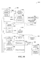
- FIG. 10 there is illustrated a block diagram of an exemplary digital camera system operable to execute the disclosed architecture.
- FIG. 10 and the following discussion are intended to provide a brief, general description of a suitable electronic computing environment 1000 in which the various aspects of the various embodiments can be implemented.
- the various embodiments described above may be suitable for application in the general context of instructions that may run or be executed in conjunction with an electronic device, those skilled in the art will recognize that the various embodiments also can be implemented in combination with other program modules and/or as a combination of hardware and software.
- program modules include routines, programs, components, data structures, etc., that perform particular tasks associated with electronic computing environment 100 .
- inventive methods can be practiced with other electronic system configurations, including hand-held computing devices, microprocessor-based or programmable consumer electronics, single-processor or multiprocessor state machines, minicomputers, as well as personal computers, and the like, each of which can be operatively coupled to one or more associated devices.
- Computer-readable media can be any available media that can be accessed by the electronic processing device and includes both volatile and nonvolatile media, removable and non-removable media.
- Computer-readable media can comprise computer storage media and communication media.
- Computer storage media can include both volatile and nonvolatile, removable and non-removable media implemented in any method or technology for storage of information such as computer-readable instructions, data structures, program modules or other data.
- Computer storage media includes, but is not limited to, RAM, ROM, EEPROM, flash memory or other memory technology, or any other medium which can be used to store the desired information and which can be accessed by the electronic processing device.
- the exemplary electronic processing environment 1000 for implementing various aspects of one or more of the various embodiments includes a digital camera 1002 , the digital camera 1002 including a system processor 1004 , optics 1006 , an image sensor 1008 , an output circuit 1010 , a signal processing circuit 1012 , a system memory 1016 and a system bus 1014 .
- the system bus 1014 couples to system components including, but not limited to, the system memory 1016 to the system processor 1004 .
- the system processor 1004 can be a suitable semiconductor processing device manufactured for digital camera 1002 , or any of various commercially available processors. Dual microprocessors and other multi-processor architectures may also be employed as the system processor 1004 .
- Optics 1006 can comprise one or more lens elements comprised of refractive material.
- the refractive material can be suitable to refract electromagnetic radiation, particularly in the visible spectrum, but also the near infrared or ultraviolet spectra, or other suitable spectra.
- optics 1006 can be configured to project and focus an image of an object onto image sensor 1008 .
- Optics can also be configured with an actuator (not depicted) to mechanically adjust optics 1006 to focus objects at varying distances from digital camera 1002 .
- Image sensor 1008 can comprise any of various sensors for receiving electromagnetic radiation and generating electric signals proportionate to a magnitude of the electromagnetic radiation.
- image sensor 1008 can comprise a video tube, a charge-coupled device, or a CMOS device, or the like, or an array of such devices.
- image sensor 1008 can comprise an array of photodetectors as described herein (e.g., optical sensor array 104 , optical sensor array 202 , optical sensor array 302 , optical sensor array 602 , etc.).
- Electric signals generated by image sensor 1008 can be transferred to output circuit 1010 , in response to a clock signal generated by an electronic clock(s) 1004 A managed by system processor 1004 . The electric signals can then be output to signal processing circuit 1012 for image processing.
- Signal processing circuit 1012 can be any suitable hardware or software processing entity, including an integrated circuit(s), an application specific integrated circuit(s) (ASIC), a state machine, or other suitable signal processing device.
- Signal processing circuit 1012 can be configured to perform operations on electric signals provided by output circuit 1010 . These operations can include correlated double sampling, gamma processing, analog to digital conversion, gain adjustment, interpolation, compression, or a combination thereof or of the like, to generate digital data to be adapted for presentation on an electronic display 1032 of digital camera 1002 . Additionally, signal processing circuit 1012 can store the digital data in system memory 1016 before, during and after the operations.
- the system bus 1014 can be any of several types of bus structure suitable for communicatively connecting components of digital camera 1002 .
- System bus 1014 can further interconnect to a memory bus (with or without a memory controller), a peripheral bus, and a local bus using any of a variety of commercially available bus architectures.
- the system memory 1016 can include read-only memory (ROM) 1020 and random access memory (RAM) 1018 .
- ROM read-only memory
- RAM random access memory
- a basic input/output system (BIOS) for digital camera 1002 can be stored in a non-volatile memory 1020 such as ROM, EPROM, EEPROM, which BIOS contains the basic routines that help to transfer information between elements within the digital camera 1002 , when powered on for instance.
- the RAM 1018 can also include a high-speed RAM such as static RAM for caching data.
- digital camera can include removable memory 1022 , which can include any suitable non-volatile memory (e.g., Flash memory), or other removable memory technology
- a number of program modules can be stored in the system memory 1016 , including an operating system 1024 , one or more application programs or program modules 1026 and program data 1028 . All or portions of the operating system, applications, modules, and/or data can also be cached in the RAM 1018 It is appreciated that the various embodiments can be implemented with various commercially available or proprietary operating systems or combinations of operating systems.
- a display 1032 is also connected to the system bus 1014 via an interface, such as a video adapter 1030 .
- Display 1032 can comprise a flat panel display, such as a liquid crystal display, a light-emitting diode display, or the like.
- System processor 1004 can control output of image data to present a digital replica of the image received by image sensor 1008 on display 1032 .
- digital camera 1002 can output the image data to an external display 1034 via a suitable external interface 1048 .
- a user can enter commands and information into the digital camera 1002 through one or more input devices, e.g., touch screen buttons, switches, dials, levers, etc.
- input devices e.g., touch screen buttons, switches, dials, levers, etc.
- zoom functionality is often implemented by pressing a button, dial, lever, etc., in one direction to zoom in, or another direction to zoom out.
- display options, selection of images, and similar display commands can be input via a touch screen, often implemented as part of display 1032 .
- Other input devices may include a microphone, an IR remote control, a joystick, a game pad, a stylus pen, or the like.
- input devices are often connected to the system processor 1004 through an input device interface 1038 that is coupled to the system bus 1014 , but can be connected by other interfaces, such as a parallel port, an IEEE1394 serial port, a game port, a USB port, an IR interface, a Bluetooth interface, etc.
- the external interface 1048 can include at least one or both of Universal Serial Bus (USB) and IEEE1394 interface technologies. Other external connection technologies are within contemplation of the subject matter claimed herein. Moreover, external interface 1048 can include a wireless technology, such as a Wi-Fi communication technology, BluetoothTM technology, infrared (IR) technology, cellular technology, or the like. In addition to an external display, external interface 1048 can facilitate communicatively coupling digital camera 1002 to one or more remote devices 1042 . Remote device(s) 1042 can include a computer, a display, a memory or storage device 1044 , and so on. Moreover, commands can be given to digital camera 1002 from remote device(s) 1042 over external interface 1048 to system processor 1004 .
- USB Universal Serial Bus
- IEEE1394 Other external connection technologies are within contemplation of the subject matter claimed herein.
- external interface 1048 can include a wireless technology, such as a Wi-Fi communication technology, BluetoothTM technology, infrared (IR) technology, cellular technology, or
- remote camera operation e.g., taking pictures, adding or deleting pictures from system memory 1016 , etc.
- data such as stored digital images, updating operation system 1024 , applications/program modules 1026 , or data 1028 , and so on.
- the digital camera 1002 can be operable to communicate with any wireless devices or entities operatively disposed in wireless communication, e.g., a printer, scanner, desktop and/or portable computer, portable data assistant, communications satellite, any piece of equipment or location associated with a wirelessly detectable tag (e.g., a kiosk, news stand, restroom), and telephone.
- any wireless devices or entities operatively disposed in wireless communication e.g., a printer, scanner, desktop and/or portable computer, portable data assistant, communications satellite, any piece of equipment or location associated with a wirelessly detectable tag (e.g., a kiosk, news stand, restroom), and telephone.
- the communication can be a predefined structure as with a conventional network or simply an ad hoc communication between at least two devices.
- Wi-Fi Wireless Fidelity
- Wi-Fi is a wireless technology similar to that used in a cell phone that enables such devices, e.g., computers, to send and receive data indoors and out; within the range of the access point.
- Wi-Fi networks use radio technologies called IEEE802.11 (a, b, g, n, etc.) to provide secure, reliable, fast wireless connectivity.
- IEEE802.11 a, b, g, n, etc.
- a Wi-Fi network can be used to connect computers to each other, to the Internet, and to wired networks (which use IEEE802.3 or Ethernet).
- Wi-Fi networks operate in the unlicensed 2.4 and 5 GHz radio bands, at an 11 Mbps (802.11a) or 54 Mbps (802.11b) data rate, for example, or with products that contain both bands (dual band), so the networks can provide real-world performance similar to the basic 10 BaseT wired Ethernet networks used in many offices.
- the terms (including a reference to a “means”) used to describe such components are intended to correspond, unless otherwise indicated, to any component which performs the specified function of the described component (e.g., a functional equivalent), even though not structurally equivalent to the disclosed structure, which performs the function in the herein illustrated exemplary aspects of the embodiments.
- the embodiments includes a system as well as a computer-readable medium having computer-executable instructions for performing the acts and/or events of the various methods.
Landscapes
- Engineering & Computer Science (AREA)
- Multimedia (AREA)
- Signal Processing (AREA)
- Transforming Light Signals Into Electric Signals (AREA)
Abstract
Description
Claims (20)
Priority Applications (1)
| Application Number | Priority Date | Filing Date | Title |
|---|---|---|---|
| US13/109,231 US8823846B2 (en) | 2011-05-17 | 2011-05-17 | Pausing digital readout of an optical sensor array |
Applications Claiming Priority (1)
| Application Number | Priority Date | Filing Date | Title |
|---|---|---|---|
| US13/109,231 US8823846B2 (en) | 2011-05-17 | 2011-05-17 | Pausing digital readout of an optical sensor array |
Publications (2)
| Publication Number | Publication Date |
|---|---|
| US20120293699A1 US20120293699A1 (en) | 2012-11-22 |
| US8823846B2 true US8823846B2 (en) | 2014-09-02 |
Family
ID=47174678
Family Applications (1)
| Application Number | Title | Priority Date | Filing Date |
|---|---|---|---|
| US13/109,231 Active 2032-08-04 US8823846B2 (en) | 2011-05-17 | 2011-05-17 | Pausing digital readout of an optical sensor array |
Country Status (1)
| Country | Link |
|---|---|
| US (1) | US8823846B2 (en) |
Cited By (5)
| Publication number | Priority date | Publication date | Assignee | Title |
|---|---|---|---|---|
| US20140316196A1 (en) * | 2013-02-28 | 2014-10-23 | Olive Medical Corporation | Videostroboscopy of vocal chords with cmos sensors |
| CN106686327A (en) * | 2016-12-28 | 2017-05-17 | 上海集成电路研发中心有限公司 | Pixel unit structure realizing three conversion gains |
| US12401911B2 (en) | 2014-11-07 | 2025-08-26 | Duelight Llc | Systems and methods for generating a high-dynamic range (HDR) pixel stream |
| US12418727B2 (en) | 2014-11-17 | 2025-09-16 | Duelight Llc | System and method for generating a digital image |
| US12445736B2 (en) | 2015-05-01 | 2025-10-14 | Duelight Llc | Systems and methods for generating a digital image |
Families Citing this family (14)
| Publication number | Priority date | Publication date | Assignee | Title |
|---|---|---|---|---|
| US7780089B2 (en) | 2005-06-03 | 2010-08-24 | Hand Held Products, Inc. | Digital picture taking optical reader having hybrid monochrome and color image sensor array |
| US7568628B2 (en) | 2005-03-11 | 2009-08-04 | Hand Held Products, Inc. | Bar code reading device with global electronic shutter control |
| US7611060B2 (en) | 2005-03-11 | 2009-11-03 | Hand Held Products, Inc. | System and method to automatically focus an image reader |
| US7770799B2 (en) | 2005-06-03 | 2010-08-10 | Hand Held Products, Inc. | Optical reader having reduced specular reflection read failures |
| CA2835870A1 (en) | 2011-05-12 | 2012-11-15 | Olive Medical Corporation | Pixel array area optimization using stacking scheme for hybrid image sensor with minimal vertical interconnects |
| US8629926B2 (en) * | 2011-11-04 | 2014-01-14 | Honeywell International, Inc. | Imaging apparatus comprising image sensor array having shared global shutter circuitry |
| US8917330B1 (en) * | 2012-06-01 | 2014-12-23 | Gopro, Inc. | Cinematic image blur in digital cameras based on exposure timing manipulation |
| US20140022431A1 (en) * | 2012-07-19 | 2014-01-23 | Nanyang Innovation & Enterprise Office | Cmos image sensor |
| CN104486987A (en) | 2012-07-26 | 2015-04-01 | 橄榄医疗公司 | Camera system with smallest area monolithic CMOS image sensor |
| US9784837B1 (en) * | 2012-08-03 | 2017-10-10 | SeeScan, Inc. | Optical ground tracking apparatus, systems, and methods |
| AU2014233192B2 (en) | 2013-03-15 | 2018-11-22 | DePuy Synthes Products, Inc. | Minimize image sensor I/O and conductor counts in endoscope applications |
| WO2014145246A1 (en) * | 2013-03-15 | 2014-09-18 | Olive Medical Corporation | Image sensor synchronization without input clock and data transmission clock |
| KR102160805B1 (en) | 2014-01-21 | 2020-09-28 | 삼성전자주식회사 | Method of correcting output signal in an image sensor |
| US11944273B2 (en) * | 2019-06-20 | 2024-04-02 | Cilag Gmbh International | Fluorescence videostroboscopy of vocal cords |
Citations (7)
| Publication number | Priority date | Publication date | Assignee | Title |
|---|---|---|---|---|
| US6888572B1 (en) | 2000-10-26 | 2005-05-03 | Rockwell Science Center, Llc | Compact active pixel with low-noise image formation |
| US7248295B2 (en) * | 2002-06-24 | 2007-07-24 | Nippon Hoso Kyokai | Image pickup apparatus including a solid-state imager having a plurality of light receptive areas |
| US7538702B2 (en) | 2007-06-15 | 2009-05-26 | Micron Technology, Inc. | Quantizing circuits with variable parameters |
| US7760250B2 (en) | 2007-06-20 | 2010-07-20 | Altasens, Inc. | Method and apparatus for minimizing noise pickup in image sensors |
| US7855748B2 (en) | 2007-12-03 | 2010-12-21 | Altasens, Inc. | Reference voltage generation in imaging sensors |
| US7930580B2 (en) | 2007-07-11 | 2011-04-19 | Altasens, Inc. | Controlling timing dependencies in a mixed signal system-on-a-chip (SOC) |
| US20110096216A1 (en) * | 2009-09-10 | 2011-04-28 | Fujifilm Corporation | Imaging pickup device and image pickup method |
-
2011
- 2011-05-17 US US13/109,231 patent/US8823846B2/en active Active
Patent Citations (7)
| Publication number | Priority date | Publication date | Assignee | Title |
|---|---|---|---|---|
| US6888572B1 (en) | 2000-10-26 | 2005-05-03 | Rockwell Science Center, Llc | Compact active pixel with low-noise image formation |
| US7248295B2 (en) * | 2002-06-24 | 2007-07-24 | Nippon Hoso Kyokai | Image pickup apparatus including a solid-state imager having a plurality of light receptive areas |
| US7538702B2 (en) | 2007-06-15 | 2009-05-26 | Micron Technology, Inc. | Quantizing circuits with variable parameters |
| US7760250B2 (en) | 2007-06-20 | 2010-07-20 | Altasens, Inc. | Method and apparatus for minimizing noise pickup in image sensors |
| US7930580B2 (en) | 2007-07-11 | 2011-04-19 | Altasens, Inc. | Controlling timing dependencies in a mixed signal system-on-a-chip (SOC) |
| US7855748B2 (en) | 2007-12-03 | 2010-12-21 | Altasens, Inc. | Reference voltage generation in imaging sensors |
| US20110096216A1 (en) * | 2009-09-10 | 2011-04-28 | Fujifilm Corporation | Imaging pickup device and image pickup method |
Cited By (9)
| Publication number | Priority date | Publication date | Assignee | Title |
|---|---|---|---|---|
| US20140316196A1 (en) * | 2013-02-28 | 2014-10-23 | Olive Medical Corporation | Videostroboscopy of vocal chords with cmos sensors |
| US10206561B2 (en) * | 2013-02-28 | 2019-02-19 | DePuy Synthes Products, Inc. | Videostroboscopy of vocal cords with CMOS sensors |
| US11266305B2 (en) * | 2013-02-28 | 2022-03-08 | DePuy Synthes Products, Inc. | Videostroboscopy of vocal cords with CMOS sensors |
| US11998166B2 (en) | 2013-02-28 | 2024-06-04 | DePuy Synthes Products, Inc. | Videostroboscopy of vocal cords with CMOS sensors |
| US12401911B2 (en) | 2014-11-07 | 2025-08-26 | Duelight Llc | Systems and methods for generating a high-dynamic range (HDR) pixel stream |
| US12418727B2 (en) | 2014-11-17 | 2025-09-16 | Duelight Llc | System and method for generating a digital image |
| US12445736B2 (en) | 2015-05-01 | 2025-10-14 | Duelight Llc | Systems and methods for generating a digital image |
| CN106686327A (en) * | 2016-12-28 | 2017-05-17 | 上海集成电路研发中心有限公司 | Pixel unit structure realizing three conversion gains |
| CN106686327B (en) * | 2016-12-28 | 2019-09-13 | 上海集成电路研发中心有限公司 | A kind of pixel cell structure for realizing three conversion gains |
Also Published As
| Publication number | Publication date |
|---|---|
| US20120293699A1 (en) | 2012-11-22 |
Similar Documents
| Publication | Publication Date | Title |
|---|---|---|
| US8823846B2 (en) | Pausing digital readout of an optical sensor array | |
| US9736405B2 (en) | Global shutter image sensor having extremely fine pitch | |
| US10136090B2 (en) | Threshold-monitoring, conditional-reset image sensor | |
| CN102857712B (en) | There is the image sensor of HDR capture capability | |
| US9124829B2 (en) | Optical black pixel readout for image sensor data correction | |
| US8300109B2 (en) | Image sensing apparatus | |
| US9006630B2 (en) | Quality of optically black reference pixels in CMOS iSoCs | |
| CN106464781B (en) | Information processing apparatus, information processing method, and computer program | |
| CN106341628A (en) | Image Sensor Having Wide Dynamic Range, Pixel Circuit Of The Image Sensor, And Operating Method Of The Image Sensor | |
| US11290648B2 (en) | Image capture apparatus and control method thereof | |
| US8896736B2 (en) | Solid-state imaging device, imaging apparatus and signal reading method having photoelectric conversion elements that are targets from which signals are read in the same group | |
| US9986163B2 (en) | Digital photographing apparatus and digital photographing method | |
| US20160037101A1 (en) | Apparatus and Method for Capturing Images | |
| US20140375861A1 (en) | Image generating apparatus and method | |
| US20180376087A1 (en) | Using the same pixels to capture both short and long exposure data for hdr image and video | |
| US9264597B2 (en) | Sensor state map for managing operational states of an image sensor | |
| US20100214441A1 (en) | Imaging apparatus | |
| US9571773B2 (en) | Drive apparatus, drive method, and electronic device | |
| WO2017101864A1 (en) | Image sensor, control method, and electronic device | |
| CN104869307B (en) | A kind of method and apparatus of shooting | |
| CN103379292B (en) | Signal handling equipment and method, imaging device and solid-state imaging element | |
| CN110832846A (en) | Pixel unit, image sensor, operating method of image sensor, and image pickup apparatus | |
| US9013624B2 (en) | Image pickup apparatus having same exposure time among pixel groups and associated method and computer-readable medium | |
| WO2017101562A1 (en) | Image sensor, terminal having same, and imaging method | |
| JP2008187614A (en) | Imaging device |
Legal Events
| Date | Code | Title | Description |
|---|---|---|---|
| AS | Assignment |
Owner name: ALTASENS, INC., CALIFORNIA Free format text: ASSIGNMENT OF ASSIGNORS INTEREST;ASSIGNORS:BLANQUART, LAURENT;WALLNER, JOHN;BHAT, MANJUNATH;SIGNING DATES FROM 20110412 TO 20110505;REEL/FRAME:026290/0570 |
|
| STCF | Information on status: patent grant |
Free format text: PATENTED CASE |
|
| FEPP | Fee payment procedure |
Free format text: ENTITY STATUS SET TO UNDISCOUNTED (ORIGINAL EVENT CODE: BIG.) |
|
| MAFP | Maintenance fee payment |
Free format text: PAYMENT OF MAINTENANCE FEE, 4TH YEAR, LARGE ENTITY (ORIGINAL EVENT CODE: M1551) Year of fee payment: 4 |
|
| AS | Assignment |
Owner name: JVC KENWOOD CORPORATION, JAPAN Free format text: ASSIGNMENT OF ASSIGNORS INTEREST;ASSIGNOR:ALTASENSE, INC;REEL/FRAME:045583/0584 Effective date: 20180307 |
|
| AS | Assignment |
Owner name: SAMSUNG ELECTRONICS CO., LTD., KOREA, REPUBLIC OF Free format text: ASSIGNMENT OF ASSIGNORS INTEREST;ASSIGNOR:JVC KENWOOD CORPORATION;REEL/FRAME:050170/0527 Effective date: 20190329 |
|
| MAFP | Maintenance fee payment |
Free format text: PAYMENT OF MAINTENANCE FEE, 8TH YEAR, LARGE ENTITY (ORIGINAL EVENT CODE: M1552); ENTITY STATUS OF PATENT OWNER: LARGE ENTITY Year of fee payment: 8 |
|
| MAFP | Maintenance fee payment |
Free format text: PAYMENT OF MAINTENANCE FEE, 12TH YEAR, LARGE ENTITY (ORIGINAL EVENT CODE: M1553); ENTITY STATUS OF PATENT OWNER: LARGE ENTITY Year of fee payment: 12 |