US8822042B2 - Luminescent cyclometallated iridium(III) complexes having acetylide ligands - Google Patents
Luminescent cyclometallated iridium(III) complexes having acetylide ligands Download PDFInfo
- Publication number
- US8822042B2 US8822042B2 US13/161,296 US201113161296A US8822042B2 US 8822042 B2 US8822042 B2 US 8822042B2 US 201113161296 A US201113161296 A US 201113161296A US 8822042 B2 US8822042 B2 US 8822042B2
- Authority
- US
- United States
- Prior art keywords
- ligand
- independently selected
- aryl
- materials
- cntbu
- Prior art date
- Legal status (The legal status is an assumption and is not a legal conclusion. Google has not performed a legal analysis and makes no representation as to the accuracy of the status listed.)
- Active, expires
Links
- 0 *.B.cc-[w]c Chemical compound *.B.cc-[w]c 0.000 description 14
- PIIOSACRICPDBQ-UHFFFAOYSA-N C[Ir](C)(C)C Chemical compound C[Ir](C)(C)C PIIOSACRICPDBQ-UHFFFAOYSA-N 0.000 description 4
- MZYDBGLUVPLRKR-UHFFFAOYSA-N C1=CC(N2C3=C(C=CC=C3)C3=C2C=CC=C3)=CC(N2C3=C(C=CC=C3)C3=C2C=CC=C3)=C1 Chemical compound C1=CC(N2C3=C(C=CC=C3)C3=C2C=CC=C3)=CC(N2C3=C(C=CC=C3)C3=C2C=CC=C3)=C1 MZYDBGLUVPLRKR-UHFFFAOYSA-N 0.000 description 3
- IBHBKWKFFTZAHE-UHFFFAOYSA-N C1=CC=C(N(C2=CC=C(C3=CC=C(N(C4=CC=CC=C4)C4=C5C=CC=CC5=CC=C4)C=C3)C=C2)C2=CC=CC3=C2C=CC=C3)C=C1 Chemical compound C1=CC=C(N(C2=CC=C(C3=CC=C(N(C4=CC=CC=C4)C4=C5C=CC=CC5=CC=C4)C=C3)C=C2)C2=CC=CC3=C2C=CC=C3)C=C1 IBHBKWKFFTZAHE-UHFFFAOYSA-N 0.000 description 3
- NSXJEEMTGWMJPY-UHFFFAOYSA-N C1=CC(N2C3=C(C=CC=C3)C3=C2C=CC=C3)=CC(C2=CC=CC(N3C4=C(C=CC=C4)C4=C3C=CC=C4)=C2)=C1 Chemical compound C1=CC(N2C3=C(C=CC=C3)C3=C2C=CC=C3)=CC(C2=CC=CC(N3C4=C(C=CC=C4)C4=C3C=CC=C4)=C2)=C1 NSXJEEMTGWMJPY-UHFFFAOYSA-N 0.000 description 2
- VFUDMQLBKNMONU-UHFFFAOYSA-N C1=CC2=C(C=C1)N(C1=CC=C(C3=CC=C(N4C5=C(C=CC=C5)C5=C4/C=C\C=C/5)C=C3)C=C1)C1=C2C=CC=C1 Chemical compound C1=CC2=C(C=C1)N(C1=CC=C(C3=CC=C(N4C5=C(C=CC=C5)C5=C4/C=C\C=C/5)C=C3)C=C1)C1=C2C=CC=C1 VFUDMQLBKNMONU-UHFFFAOYSA-N 0.000 description 2
- SDEFDICGRVDKPH-UHFFFAOYSA-M C1=CC2=C3C(=C1)O[AlH]/N3=C/C=C\2 Chemical compound C1=CC2=C3C(=C1)O[AlH]/N3=C/C=C\2 SDEFDICGRVDKPH-UHFFFAOYSA-M 0.000 description 2
- DHDHJYNTEFLIHY-UHFFFAOYSA-N C1=CC=C(C2=CC=NC3=C2C=CC2=C3N=CC=C2C2=CC=CC=C2)C=C1 Chemical compound C1=CC=C(C2=CC=NC3=C2C=CC2=C3N=CC=C2C2=CC=CC=C2)C=C1 DHDHJYNTEFLIHY-UHFFFAOYSA-N 0.000 description 2
- IEGZNIQHTJNUPB-UHFFFAOYSA-N C1=CC=C(C2=NC3=C(C=C2)C2=C(N=CC=C2)/C2=N\C=C/C=C\32)C=C1 Chemical compound C1=CC=C(C2=NC3=C(C=C2)C2=C(N=CC=C2)/C2=N\C=C/C=C\32)C=C1 IEGZNIQHTJNUPB-UHFFFAOYSA-N 0.000 description 2
- GEQBRULPNIVQPP-UHFFFAOYSA-N C1=CC=C(N2C(C3=CC(/C4=N/C5=C(C=CC=C5)N4C4=CC=CC=C4)=CC(/C4=N/C5=C(C=CC=C5)N4C4=CC=CC=C4)=C3)=NC3=C2C=CC=C3)C=C1 Chemical compound C1=CC=C(N2C(C3=CC(/C4=N/C5=C(C=CC=C5)N4C4=CC=CC=C4)=CC(/C4=N/C5=C(C=CC=C5)N4C4=CC=CC=C4)=C3)=NC3=C2C=CC=C3)C=C1 GEQBRULPNIVQPP-UHFFFAOYSA-N 0.000 description 2
- RPHSQWOMKHJGSI-UHFFFAOYSA-N C1=CC=C(N2C3=C(C=C(C4=CC=CC(C5=CC6=C(C=C5)N(C5=CC=CC=C5)C5=C6C=C(C6=C\C7=C(\C=C/6)C6=C(C=CN=C6)O7)C=C5)=C4)C=C3)C3=C2C=CC(C2=CC=C4C(=C2)OC2=C4C=NC=C2)=C3)C=C1 Chemical compound C1=CC=C(N2C3=C(C=C(C4=CC=CC(C5=CC6=C(C=C5)N(C5=CC=CC=C5)C5=C6C=C(C6=C\C7=C(\C=C/6)C6=C(C=CN=C6)O7)C=C5)=C4)C=C3)C3=C2C=CC(C2=CC=C4C(=C2)OC2=C4C=NC=C2)=C3)C=C1 RPHSQWOMKHJGSI-UHFFFAOYSA-N 0.000 description 2
- LYXTZYYMWXCIFZ-UHFFFAOYSA-N C1=CC=C2C(=C1)C1=C(C=CC=C1)C2(C1=CC=C(OC2=CC=C(N3C4=C(C=CC=C4)C4=C3C=CC=C4)C=C2)C=C1)C1=CC=C(OC2=CC=C(N3C4=C(C=CC=C4)C4=C3C=CC=C4)C=C2)C=C1 Chemical compound C1=CC=C2C(=C1)C1=C(C=CC=C1)C2(C1=CC=C(OC2=CC=C(N3C4=C(C=CC=C4)C4=C3C=CC=C4)C=C2)C=C1)C1=CC=C(OC2=CC=C(N3C4=C(C=CC=C4)C4=C3C=CC=C4)C=C2)C=C1 LYXTZYYMWXCIFZ-UHFFFAOYSA-N 0.000 description 2
- XZCJVWCMJYNSQO-UHFFFAOYSA-N CC(C)(C)C1=CC=C(C2=NN=C(C3=CC=C(C4=CC=CC=C4)C=C3)O2)C=C1 Chemical compound CC(C)(C)C1=CC=C(C2=NN=C(C3=CC=C(C4=CC=CC=C4)C=C3)O2)C=C1 XZCJVWCMJYNSQO-UHFFFAOYSA-N 0.000 description 2
- XYYYIVRDTLXJEF-UHFFFAOYSA-L CC1=N2/C3=C(C=CC=C3O[Al]2OC2=CC=C(C3=CC=CC=C3)C=C2)/C=C\1 Chemical compound CC1=N2/C3=C(C=CC=C3O[Al]2OC2=CC=C(C3=CC=CC=C3)C=C2)/C=C\1 XYYYIVRDTLXJEF-UHFFFAOYSA-L 0.000 description 2
- STTGYIUESPWXOW-UHFFFAOYSA-N CC1=NC2=C(C=CC3=C2N=C(C)C=C3C2=CC=CC=C2)C(C2=CC=CC=C2)=C1 Chemical compound CC1=NC2=C(C=CC3=C2N=C(C)C=C3C2=CC=CC=C2)C(C2=CC=CC=C2)=C1 STTGYIUESPWXOW-UHFFFAOYSA-N 0.000 description 2
- AYOMISFIGMZTGF-UHFFFAOYSA-N BrC1=CC=C(N(C2=CC=C(N(C3=C4C=CC=CC4=C4C=CC=CC4=C3)C3=C4C=CC=CC4=C4C=CC=CC4=C3)C=C2)C2=C3C=CC=CC3=C3C=CC=CC3=C2)C=C1 Chemical compound BrC1=CC=C(N(C2=CC=C(N(C3=C4C=CC=CC4=C4C=CC=CC4=C3)C3=C4C=CC=CC4=C4C=CC=CC4=C3)C=C2)C2=C3C=CC=CC3=C3C=CC=CC3=C2)C=C1 AYOMISFIGMZTGF-UHFFFAOYSA-N 0.000 description 1
- FSZHBEYFUBAVJU-UHFFFAOYSA-N C(#C[Au]12C3=CC=CC=C3C3=CC=CC(=N31)C1=CC=CC=C12)C1=CC=C(N(C2=CC=CC=C2)C2=CC=CC=C2)C=C1 Chemical compound C(#C[Au]12C3=CC=CC=C3C3=CC=CC(=N31)C1=CC=CC=C12)C1=CC=C(N(C2=CC=CC=C2)C2=CC=CC=C2)C=C1 FSZHBEYFUBAVJU-UHFFFAOYSA-N 0.000 description 1
- NHDZESQHWMKRPE-UHFFFAOYSA-N C.C.CCC Chemical compound C.C.CCC NHDZESQHWMKRPE-UHFFFAOYSA-N 0.000 description 1
- KIMKXMLJSIOUQK-UHFFFAOYSA-M C.CC(C)(C)N#C[Ir](C)(C)(N)(N)C#C[Ar].CC(C)(C)N#C[Ir](C)(C)(N)(N)OS(=O)(=O)C(F)(F)F.N.[H]C#C[Ar] Chemical compound C.CC(C)(C)N#C[Ir](C)(C)(N)(N)C#C[Ar].CC(C)(C)N#C[Ir](C)(C)(N)(N)OS(=O)(=O)C(F)(F)F.N.[H]C#C[Ar] KIMKXMLJSIOUQK-UHFFFAOYSA-M 0.000 description 1
- NIIGBGBHHCKISS-UHFFFAOYSA-L C.CC(C)(C)N#C[Ir](C)(C)(N)(N)Cl.CC(C)(C)N#C[Ir](C)(C)(N)(N)OS(=O)(=O)C(F)(F)F.C[Ir]1(C)(N)(N)Cl[Ir](C)(C)(N)(N)Cl1.N.O=[Ag]S(=O)(=O)C(F)(F)F.[C-]#[N+]C(C)(C)C Chemical compound C.CC(C)(C)N#C[Ir](C)(C)(N)(N)Cl.CC(C)(C)N#C[Ir](C)(C)(N)(N)OS(=O)(=O)C(F)(F)F.C[Ir]1(C)(N)(N)Cl[Ir](C)(C)(N)(N)Cl1.N.O=[Ag]S(=O)(=O)C(F)(F)F.[C-]#[N+]C(C)(C)C NIIGBGBHHCKISS-UHFFFAOYSA-L 0.000 description 1
- OYHMICVXESLDLF-UHFFFAOYSA-N C.C[Ir](C)(C)(C)(N)N.C[Ir](C)(N)(N)(C#C[Ar])C#C[Ar].N.[H]C#C[Ar] Chemical compound C.C[Ir](C)(C)(C)(N)N.C[Ir](C)(N)(N)(C#C[Ar])C#C[Ar].N.[H]C#C[Ar] OYHMICVXESLDLF-UHFFFAOYSA-N 0.000 description 1
- NUXBKSJBZXUTFK-UHFFFAOYSA-N C.C[Ir](C)(C)(C)(N)N.C[Ir]1(C)(N)(N)Cl[Ir](C)(C)(N)(N)Cl1.N.O=[Ag]S(=O)(=O)C(F)(F)F Chemical compound C.C[Ir](C)(C)(C)(N)N.C[Ir]1(C)(N)(N)Cl[Ir](C)(C)(N)(N)Cl1.N.O=[Ag]S(=O)(=O)C(F)(F)F NUXBKSJBZXUTFK-UHFFFAOYSA-N 0.000 description 1
- FEEVDOPOKYHDKB-UHFFFAOYSA-N C1=CC(C2=CC3=C(C=C2)C2=C(C=CC=C2)C2=C3C=CC=C2)=CC(C2=CC3=C(C=C2)C2=C(C=CC=C2)C2=C3C=CC=C2)=C1 Chemical compound C1=CC(C2=CC3=C(C=C2)C2=C(C=CC=C2)C2=C3C=CC=C2)=CC(C2=CC3=C(C=C2)C2=C(C=CC=C2)C2=C3C=CC=C2)=C1 FEEVDOPOKYHDKB-UHFFFAOYSA-N 0.000 description 1
- IMKXSEPQICZHSL-UHFFFAOYSA-N C1=CC(C2=CC3=C(C=C2)SC2=C3C=CC=C2)=CC(C2=CC(N3C4=C(C=CC=C4)C4=C3C=CC=C4)=CC=C2)=C1 Chemical compound C1=CC(C2=CC3=C(C=C2)SC2=C3C=CC=C2)=CC(C2=CC(N3C4=C(C=CC=C4)C4=C3C=CC=C4)=CC=C2)=C1 IMKXSEPQICZHSL-UHFFFAOYSA-N 0.000 description 1
- QKVWPNRUXZYLQV-UHFFFAOYSA-N C1=CC(C2=CC=C3C(=C2)C2=C(C=CC=C2)C2=C3C=CC=C2)=CC(C2=CC=CC3=C2SC2=C3C=CC=C2)=C1 Chemical compound C1=CC(C2=CC=C3C(=C2)C2=C(C=CC=C2)C2=C3C=CC=C2)=CC(C2=CC=CC3=C2SC2=C3C=CC=C2)=C1 QKVWPNRUXZYLQV-UHFFFAOYSA-N 0.000 description 1
- KFKHNBPNJMWUEG-UHFFFAOYSA-N C1=CC(C2=CC=CC(C3=CC4=C(C=C3)C3=C(C=CC=C3)C3=C4C=CC=C3)=C2)=CC(C2=CC3=C(C=C2)C2=C(C=CC=C2)C2=C3C=CC=C2)=C1 Chemical compound C1=CC(C2=CC=CC(C3=CC4=C(C=C3)C3=C(C=CC=C3)C3=C4C=CC=C3)=C2)=CC(C2=CC3=C(C=C2)C2=C(C=CC=C2)C2=C3C=CC=C2)=C1 KFKHNBPNJMWUEG-UHFFFAOYSA-N 0.000 description 1
- IHUZMIYPBUPXCM-UHFFFAOYSA-N C1=CC2=C(C=C1)C1=C(/C=C\C(N3C4=C(C=CC=C4)C4=C3/C=C/C(N3C5=C(C=CC=C5)C5=C3/C=C\C=C/5)=C\4)=C/1)S2 Chemical compound C1=CC2=C(C=C1)C1=C(/C=C\C(N3C4=C(C=CC=C4)C4=C3/C=C/C(N3C5=C(C=CC=C5)C5=C3/C=C\C=C/5)=C\4)=C/1)S2 IHUZMIYPBUPXCM-UHFFFAOYSA-N 0.000 description 1
- HSPZYQUMRCQDDG-UHFFFAOYSA-N C1=CC2=C(C=C1)C1=CC=C3[Ir]N4=C(C=CC=C4)C3=C1S2 Chemical compound C1=CC2=C(C=C1)C1=CC=C3[Ir]N4=C(C=CC=C4)C3=C1S2 HSPZYQUMRCQDDG-UHFFFAOYSA-N 0.000 description 1
- RRVDTWKWNCCQAM-UHFFFAOYSA-N C1=CC2=C(C=C1)C1=C\C=C/C=C\1C2.CC1=C2C=C3C=CC=CC3=CC2=CC=C1.CC1=C2C=CC=CC2=CC2=CC=CC=C21.CC1=CC2=C(C=C1)C1=C(C=CC=C1)C1=C2C=CC=N1.CC1=CC2=C(C=C1)C1=C(N=CC=C1)C1=C2C=CC=C1.CC1=CC2=C(C=C1)C1=C(N=CC=N1)C1=C2C=CC=C1.CC1=CC2=C(C=C1)C=CC1=C2N=CC=C1.CC1=CC2=C(C=CC=C2)C2=C1C=CC=N2.CC1=CC2=C(N=C1)C1=C(C=CC=C1)C=C2.CC1=CC2=C(N=CC=C2)C2=C1C=CC=C2.CC1=CC2=C(N=CC=C2)C2=C1C=CC=N2.CC1=CC=C2C=C3C=CC=CC3=CC2=C1.CC1=CC=CC2=C1C1=C(N=CC=N1)C1=C2C=CC=C1.CC1=NC2=C(C=C1)C1=C(C=CC=C1)C1=C2C=CC=C1.CC1=NC2=C(C=C1)C=CC1=C2C=CC=C1.CN1C2=C(C=CC=C2)C2=C\C=C/C=C\21 Chemical compound C1=CC2=C(C=C1)C1=C\C=C/C=C\1C2.CC1=C2C=C3C=CC=CC3=CC2=CC=C1.CC1=C2C=CC=CC2=CC2=CC=CC=C21.CC1=CC2=C(C=C1)C1=C(C=CC=C1)C1=C2C=CC=N1.CC1=CC2=C(C=C1)C1=C(N=CC=C1)C1=C2C=CC=C1.CC1=CC2=C(C=C1)C1=C(N=CC=N1)C1=C2C=CC=C1.CC1=CC2=C(C=C1)C=CC1=C2N=CC=C1.CC1=CC2=C(C=CC=C2)C2=C1C=CC=N2.CC1=CC2=C(N=C1)C1=C(C=CC=C1)C=C2.CC1=CC2=C(N=CC=C2)C2=C1C=CC=C2.CC1=CC2=C(N=CC=C2)C2=C1C=CC=N2.CC1=CC=C2C=C3C=CC=CC3=CC2=C1.CC1=CC=CC2=C1C1=C(N=CC=N1)C1=C2C=CC=C1.CC1=NC2=C(C=C1)C1=C(C=CC=C1)C1=C2C=CC=C1.CC1=NC2=C(C=C1)C=CC1=C2C=CC=C1.CN1C2=C(C=CC=C2)C2=C\C=C/C=C\21 RRVDTWKWNCCQAM-UHFFFAOYSA-N 0.000 description 1
- SDHNJSIZTIODFW-UHFFFAOYSA-N C1=CC2=C(C=C1)N(C1=CC3=C(C=C1)SC1=C3/C=C(N3C4=C(C=CC=C4)C4=C3C=CC=C4)\C=C/1)C1=C2C=CC=C1 Chemical compound C1=CC2=C(C=C1)N(C1=CC3=C(C=C1)SC1=C3/C=C(N3C4=C(C=CC=C4)C4=C3C=CC=C4)\C=C/1)C1=C2C=CC=C1 SDHNJSIZTIODFW-UHFFFAOYSA-N 0.000 description 1
- AWXGSYPUMWKTBR-UHFFFAOYSA-N C1=CC2=C(C=C1)N(C1=CC=C(N(C3=CC=C(N4C5=C(C=CC=C5)C5=C4C=CC=C5)C=C3)C3=CC=C(N4C5=C(C=CC=C5)C5=C4C=CC=C5)C=C3)C=C1)C1=C2C=CC=C1 Chemical compound C1=CC2=C(C=C1)N(C1=CC=C(N(C3=CC=C(N4C5=C(C=CC=C5)C5=C4C=CC=C5)C=C3)C3=CC=C(N4C5=C(C=CC=C5)C5=C4C=CC=C5)C=C3)C=C1)C1=C2C=CC=C1 AWXGSYPUMWKTBR-UHFFFAOYSA-N 0.000 description 1
- JTXCFSSIPVHVHI-UHFFFAOYSA-M C1=CC2=C(C=C1)N1=C(O2)C2=C\C=C/C=C\2O[Zn]1 Chemical compound C1=CC2=C(C=C1)N1=C(O2)C2=C\C=C/C=C\2O[Zn]1 JTXCFSSIPVHVHI-UHFFFAOYSA-M 0.000 description 1
- IPHJBEMZJPBDDQ-UHFFFAOYSA-M C1=CC2=C(C=C1)N1=C(S2)C2=C\C=C/C=C\2O[Zn]1 Chemical compound C1=CC2=C(C=C1)N1=C(S2)C2=C\C=C/C=C\2O[Zn]1 IPHJBEMZJPBDDQ-UHFFFAOYSA-M 0.000 description 1
- CQZOLIZFWRSNOM-UHFFFAOYSA-N C1=CC2=C(C=C1)N1CC3=CC=CC4=C3[Ir]35(C6=CN(CC7=CC=CC(=N73)CN3C=C5C5=C3C=CC=C5)C3=C6C=CC=C3)(N1=C2)N1=CC2=C(C=CC=C2)N1C4 Chemical compound C1=CC2=C(C=C1)N1CC3=CC=CC4=C3[Ir]35(C6=CN(CC7=CC=CC(=N73)CN3C=C5C5=C3C=CC=C5)C3=C6C=CC=C3)(N1=C2)N1=CC2=C(C=CC=C2)N1C4 CQZOLIZFWRSNOM-UHFFFAOYSA-N 0.000 description 1
- VDRONIBNVZLDJL-UHFFFAOYSA-N C1=CC2=C(SC3=C2/C=C\C=C/3N2C3=C(C=CC=C3)C3=C2C=CC=C3)C(N2C3=C(C=CC=C3)C3=C2C=CC=C3)=C1 Chemical compound C1=CC2=C(SC3=C2/C=C\C=C/3N2C3=C(C=CC=C3)C3=C2C=CC=C3)C(N2C3=C(C=CC=C3)C3=C2C=CC=C3)=C1 VDRONIBNVZLDJL-UHFFFAOYSA-N 0.000 description 1
- SBYMPPVIXIJQGA-UHFFFAOYSA-N C1=CC2=C3C4=C1C1=C5C4=C4C6=C\3C3=C2C=CC2=C3/C3=C\6C6=C4/C4=C5/C(=C5/C=C\C7=C8C=CC2=C3C8=C/6/C7=C/54)/C=C\1 Chemical compound C1=CC2=C3C4=C1C1=C5C4=C4C6=C\3C3=C2C=CC2=C3/C3=C\6C6=C4/C4=C5/C(=C5/C=C\C7=C8C=CC2=C3C8=C/6/C7=C/54)/C=C\1 SBYMPPVIXIJQGA-UHFFFAOYSA-N 0.000 description 1
- LABGHJUTWCOYQE-UHFFFAOYSA-N C1=CC2=CC=C(C3=CC4=C(C=C3)C=C(C3=CC=CC(C5=C6/C=C\C=C/C6=C6C=CC=CC6=C5)=C3)C=C4)C=C2C=C1 Chemical compound C1=CC2=CC=C(C3=CC4=C(C=C3)C=C(C3=CC=CC(C5=C6/C=C\C=C/C6=C6C=CC=CC6=C5)=C3)C=C4)C=C2C=C1 LABGHJUTWCOYQE-UHFFFAOYSA-N 0.000 description 1
- LOANKKZXVZMPBA-UHFFFAOYSA-N C1=CC=C(C2=C/C3=C(/C=C/2)[Ir]N2=CC=CN32)C=C1 Chemical compound C1=CC=C(C2=C/C3=C(/C=C/2)[Ir]N2=CC=CN32)C=C1 LOANKKZXVZMPBA-UHFFFAOYSA-N 0.000 description 1
- ABFTVLCDLFSSMI-UHFFFAOYSA-N C1=CC=C(C2=CC3=C(C=C2)[Ir]2(C4=CC=CC=C4C4=N2C=CC=C4)N2=CC=CC=C32)C=C1 Chemical compound C1=CC=C(C2=CC3=C(C=C2)[Ir]2(C4=CC=CC=C4C4=N2C=CC=C4)N2=CC=CC=C32)C=C1 ABFTVLCDLFSSMI-UHFFFAOYSA-N 0.000 description 1
- RSWOJEDGRFCGFR-UHFFFAOYSA-N C1=CC=C(C2=CC3=C(C=C2C2=CC=CC=C2)C2=C(C=C(C4=CC=CC=C4)C(C4=CC=CC=C4)=C2)C2=C3C=C(C3=CC=CC=C3)C(C3=CC=CC=C3)=C2)C=C1 Chemical compound C1=CC=C(C2=CC3=C(C=C2C2=CC=CC=C2)C2=C(C=C(C4=CC=CC=C4)C(C4=CC=CC=C4)=C2)C2=C3C=C(C3=CC=CC=C3)C(C3=CC=CC=C3)=C2)C=C1 RSWOJEDGRFCGFR-UHFFFAOYSA-N 0.000 description 1
- WXAIEIRYBSKHDP-UHFFFAOYSA-N C1=CC=C(C2=CC=C(N(C3=CC=C(C4=CC=CC=C4)C=C3)C3=CC=C(C4=CC=C(N(C5=CC=C(C6=CC=CC=C6)C=C5)C5=CC=C(C6=CC=CC=C6)C=C5)C=C4)C=C3)C=C2)C=C1 Chemical compound C1=CC=C(C2=CC=C(N(C3=CC=C(C4=CC=CC=C4)C=C3)C3=CC=C(C4=CC=C(N(C5=CC=C(C6=CC=CC=C6)C=C5)C5=CC=C(C6=CC=CC=C6)C=C5)C=C4)C=C3)C=C2)C=C1 WXAIEIRYBSKHDP-UHFFFAOYSA-N 0.000 description 1
- KQCREFMBDCFFGP-UHFFFAOYSA-N C1=CC=C(C2=CC=C(N(C3=CC=CC=C3)C3=CC=C(C4=CC=C(N(C5=CC=CC=C5)C5=CC=C(C6=CC=C(C7=CC=C(N(C8=CC=CC=C8)C8=CC=C(C9=CC=C(N(C%10=CC=CC=C%10)C%10=CC=C(C%11=CC=CC=C%11)C=C%10)C=C9)C=C8)C=C7)C=C6)C=C5)C=C4)C=C3)C=C2)C=C1 Chemical compound C1=CC=C(C2=CC=C(N(C3=CC=CC=C3)C3=CC=C(C4=CC=C(N(C5=CC=CC=C5)C5=CC=C(C6=CC=C(C7=CC=C(N(C8=CC=CC=C8)C8=CC=C(C9=CC=C(N(C%10=CC=CC=C%10)C%10=CC=C(C%11=CC=CC=C%11)C=C%10)C=C9)C=C8)C=C7)C=C6)C=C5)C=C4)C=C3)C=C2)C=C1 KQCREFMBDCFFGP-UHFFFAOYSA-N 0.000 description 1
- HTNRLCWDKMRUIH-UHFFFAOYSA-N C1=CC=C(C2=CC=N3C4=C2/C=C\C2=C(C5=CC=CC=C5)C=CN(=C24)[Pt]3(C2=CC=CC=C2)C2=CC=CC=C2)C=C1.CF.CF.FF.FF.FF.FF Chemical compound C1=CC=C(C2=CC=N3C4=C2/C=C\C2=C(C5=CC=CC=C5)C=CN(=C24)[Pt]3(C2=CC=CC=C2)C2=CC=CC=C2)C=C1.CF.CF.FF.FF.FF.FF HTNRLCWDKMRUIH-UHFFFAOYSA-N 0.000 description 1
- VBJWDGGEJNGTET-UHFFFAOYSA-N C1=CC=C(C2=NC(C3=CC=CC=C3)=NC(N3C4=C(C=CC=C4)C4=CC=C5C6=C(C=CC=C6)N(C6=CC=CC=C6)C5=C43)=N2)C=C1 Chemical compound C1=CC=C(C2=NC(C3=CC=CC=C3)=NC(N3C4=C(C=CC=C4)C4=CC=C5C6=C(C=CC=C6)N(C6=CC=CC=C6)C5=C43)=N2)C=C1 VBJWDGGEJNGTET-UHFFFAOYSA-N 0.000 description 1
- PHBJYIUTTPNUBD-UHFFFAOYSA-N C1=CC=C(C2=NC3=C(C=CC=C3)N2C2=CC=C(C3=C4C=CC=CC4=C(C4=CC=C5C=CC=CC5=C4)C4=C3C=CC=C4)C=C2)C=C1 Chemical compound C1=CC=C(C2=NC3=C(C=CC=C3)N2C2=CC=C(C3=C4C=CC=CC4=C(C4=CC=C5C=CC=CC5=C4)C4=C3C=CC=C4)C=C2)C=C1 PHBJYIUTTPNUBD-UHFFFAOYSA-N 0.000 description 1
- YRWIIMMGRRUDQF-UHFFFAOYSA-P C1=CC=C(C2=NN3C(=N2)C2=CC=CC=N2[Cu]32[PH](C3=CC=CC=C3)(C3=CC=CC=C3)C3=CC=CC=C3OC3=C(C=CC=C3)[PH]2(C2=CC=CC=C2)C2=CC=CC=C2)C=C1 Chemical compound C1=CC=C(C2=NN3C(=N2)C2=CC=CC=N2[Cu]32[PH](C3=CC=CC=C3)(C3=CC=CC=C3)C3=CC=CC=C3OC3=C(C=CC=C3)[PH]2(C2=CC=CC=C2)C2=CC=CC=C2)C=C1 YRWIIMMGRRUDQF-UHFFFAOYSA-P 0.000 description 1
- ICVRMAPETUQKIA-UHFFFAOYSA-N C1=CC=C(C2=NN=C(C3=CC=C(C4=NN=C(C5=CC=CC=C5)N4C4=CC=CC=C4)C=C3)O2)C=C1 Chemical compound C1=CC=C(C2=NN=C(C3=CC=C(C4=NN=C(C5=CC=CC=C5)N4C4=CC=CC=C4)C=C3)O2)C=C1 ICVRMAPETUQKIA-UHFFFAOYSA-N 0.000 description 1
- AOQKGYRILLEVJV-UHFFFAOYSA-N C1=CC=C(C2=NN=C(C3=CC=CC=C3)N2C2=CC=CC3=C2C=CC=C3)C=C1 Chemical compound C1=CC=C(C2=NN=C(C3=CC=CC=C3)N2C2=CC=CC3=C2C=CC=C3)C=C1 AOQKGYRILLEVJV-UHFFFAOYSA-N 0.000 description 1
- RZKBYYWKDPFCMX-UHFFFAOYSA-N C1=CC=C(N(C2=CC=C(C3=CC=C(N(C4=CC=CC=C4)C4=C5SC6=C(C=CC=C6)C5=CC=C4)C=C3)C=C2)C2=CC=CC3=C2SC2=C3C=CC=C2)C=C1 Chemical compound C1=CC=C(N(C2=CC=C(C3=CC=C(N(C4=CC=CC=C4)C4=C5SC6=C(C=CC=C6)C5=CC=C4)C=C3)C=C2)C2=CC=CC3=C2SC2=C3C=CC=C2)C=C1 RZKBYYWKDPFCMX-UHFFFAOYSA-N 0.000 description 1
- CRHRWHRNQKPUPO-UHFFFAOYSA-N C1=CC=C(N(C2=CC=C(N(C3=CC=C(N(C4=CC=CC=C4)C4=C5C=CC=CC5=CC=C4)C=C3)C3=CC=C(N(C4=CC=CC=C4)C4=C5C=CC=CC5=CC=C4)C=C3)C=C2)C2=C3C=CC=CC3=CC=C2)C=C1 Chemical compound C1=CC=C(N(C2=CC=C(N(C3=CC=C(N(C4=CC=CC=C4)C4=C5C=CC=CC5=CC=C4)C=C3)C3=CC=C(N(C4=CC=CC=C4)C4=C5C=CC=CC5=CC=C4)C=C3)C=C2)C2=C3C=CC=CC3=CC=C2)C=C1 CRHRWHRNQKPUPO-UHFFFAOYSA-N 0.000 description 1
- JFKLZFRYTVUCFU-MVVLPMFXSA-N C1=CC=C(N(C2=CC=C3C(=C2)C2=CC=CC=C2C2=C(C=CC=C2)C2=C3C=CC=C2)C2=CC3=C(C=C2)C2=CC=CC=C2C2=CC=CC=C2C2=C3C=CC=C2)C=C1 Chemical compound C1=CC=C(N(C2=CC=C3C(=C2)C2=CC=CC=C2C2=C(C=CC=C2)C2=C3C=CC=C2)C2=CC3=C(C=C2)C2=CC=CC=C2C2=CC=CC=C2C2=C3C=CC=C2)C=C1 JFKLZFRYTVUCFU-MVVLPMFXSA-N 0.000 description 1
- WLLRHFOXFKWDMQ-UHFFFAOYSA-N C1=CC=C(N(C2=CC=CC=C2)C2=CC=C(C3=CC=C(N(C4=CC=CC=C4)C4=CC=C(C5=CC=C(N(C6=CC=CC=C6)C6=CC=C(C7=CC=C(N(C8=CC=CC=C8)C8=CC=CC=C8)C=C7)C=C6)C=C5)C=C4)C=C3)C=C2)C=C1 Chemical compound C1=CC=C(N(C2=CC=CC=C2)C2=CC=C(C3=CC=C(N(C4=CC=CC=C4)C4=CC=C(C5=CC=C(N(C6=CC=CC=C6)C6=CC=C(C7=CC=C(N(C8=CC=CC=C8)C8=CC=CC=C8)C=C7)C=C6)C=C5)C=C4)C=C3)C=C2)C=C1 WLLRHFOXFKWDMQ-UHFFFAOYSA-N 0.000 description 1
- OWGROPIUHIMXLC-UHFFFAOYSA-L C1=CC=C(N(C2=CC=CC=C2)C2=CC=C(O[Al]3OC4=C/C=C\C=C\4C4=N3C3=C(C=CC=C3)O4)C=C2)C=C1 Chemical compound C1=CC=C(N(C2=CC=CC=C2)C2=CC=C(O[Al]3OC4=C/C=C\C=C\4C4=N3C3=C(C=CC=C3)O4)C=C2)C=C1 OWGROPIUHIMXLC-UHFFFAOYSA-L 0.000 description 1
- VOZBMWWMIQGZGM-UHFFFAOYSA-N C1=CC=C(N2C3=C(C=CC=C3)/N=C\2C2=CC=C(C3=CC4=C(C5=CC6=C(C=CC=C6)C=C5)C5=CC=CC=C5C(C5=CC=C6C=CC=CC6=C5)=C4C=C3)C=C2)C=C1 Chemical compound C1=CC=C(N2C3=C(C=CC=C3)/N=C\2C2=CC=C(C3=CC4=C(C5=CC6=C(C=CC=C6)C=C5)C5=CC=CC=C5C(C5=CC=C6C=CC=CC6=C5)=C4C=C3)C=C2)C=C1 VOZBMWWMIQGZGM-UHFFFAOYSA-N 0.000 description 1
- PFDGGTXOJGJINX-UHFFFAOYSA-N C1=CC=C(N2C3=C(C=CC=C3)N3=C2C2=C\C=C/C=C\2[Ir]3)C=C1 Chemical compound C1=CC=C(N2C3=C(C=CC=C3)N3=C2C2=C\C=C/C=C\2[Ir]3)C=C1 PFDGGTXOJGJINX-UHFFFAOYSA-N 0.000 description 1
- IIBIMTHLGUGVJF-UHFFFAOYSA-N C1=CC=C(N2C3=C(C=CC=C3)N3C4=C(/C=C/C=C/4)[Ir]C23)C=C1 Chemical compound C1=CC=C(N2C3=C(C=CC=C3)N3C4=C(/C=C/C=C/4)[Ir]C23)C=C1 IIBIMTHLGUGVJF-UHFFFAOYSA-N 0.000 description 1
- ILBCEHBXGSOZJK-UHFFFAOYSA-N C1=CC=C(N2C3=CC=CC=C3C3=C2C2=C(C=C3)C3=C(C=CC=C3)N2C2=CC=C(N3C4=C(C=CC=C4)C4=C3C3=C(C=C4)C4=CC=CC=C4N3C3=CC=CC=C3)C=C2)C=C1 Chemical compound C1=CC=C(N2C3=CC=CC=C3C3=C2C2=C(C=C3)C3=C(C=CC=C3)N2C2=CC=C(N3C4=C(C=CC=C4)C4=C3C3=C(C=C4)C4=CC=CC=C4N3C3=CC=CC=C3)C=C2)C=C1 ILBCEHBXGSOZJK-UHFFFAOYSA-N 0.000 description 1
- FLCOBMXLSOVHGE-UHFFFAOYSA-N C1=CC=C(N2C3=CC=CC=C3C3=C2C2=C(C=C3)C3=C(C=CC=C3)N2C2=CC=CC=C2)C=C1 Chemical compound C1=CC=C(N2C3=CC=CC=C3C3=C2C2=C(C=C3)C3=C(C=CC=C3)N2C2=CC=CC=C2)C=C1 FLCOBMXLSOVHGE-UHFFFAOYSA-N 0.000 description 1
- KSJBCQHLUVQQRU-UHFFFAOYSA-N C1=CC=C(N2C3=CC=CC=C3C3=CC4=C(C=C32)[Ir]N2=C4C=CC=C2)C=C1 Chemical compound C1=CC=C(N2C3=CC=CC=C3C3=CC4=C(C=C32)[Ir]N2=C4C=CC=C2)C=C1 KSJBCQHLUVQQRU-UHFFFAOYSA-N 0.000 description 1
- VNTLICYURVZKBN-UHFFFAOYSA-N C1=CC=C(N2C=CN3=C2C2=C\C=C/C=C\2[Ir]3)C=C1 Chemical compound C1=CC=C(N2C=CN3=C2C2=C\C=C/C=C\2[Ir]3)C=C1 VNTLICYURVZKBN-UHFFFAOYSA-N 0.000 description 1
- ROBUGAOOQWWSQP-UHFFFAOYSA-L C1=CC=C(O[Al]2OC3=C/C=C\C=C\3C3=N2C2=C(C=CC=C2)O3)C=C1 Chemical compound C1=CC=C(O[Al]2OC3=C/C=C\C=C\3C3=N2C2=C(C=CC=C2)O3)C=C1 ROBUGAOOQWWSQP-UHFFFAOYSA-L 0.000 description 1
- ASWCTGBIMZWXAP-UHFFFAOYSA-M C1=CC=C(O[Pt]23C4=C(C=CC=C4C4=CC=CC=N42)C2=CC=CC=N23)C=C1 Chemical compound C1=CC=C(O[Pt]23C4=C(C=CC=C4C4=CC=CC=N42)C2=CC=CC=N23)C=C1 ASWCTGBIMZWXAP-UHFFFAOYSA-M 0.000 description 1
- MKZDOOLFFBQAOV-UHFFFAOYSA-N C1=CC=C(P(C2=CC=CC=C2)C2=CC=CC=C2)C=C1.C1=NN2[Os]N3=C(/C=C\C=C/3)C2=C1 Chemical compound C1=CC=C(P(C2=CC=CC=C2)C2=CC=CC=C2)C=C1.C1=NN2[Os]N3=C(/C=C\C=C/3)C2=C1 MKZDOOLFFBQAOV-UHFFFAOYSA-N 0.000 description 1
- RNJALDUDQIQBDE-UHFFFAOYSA-N C1=CC=C([Si](C2=CC=CC=C2)(C2=CC=CC(C3=C4SC5=C(C=CC=C5)C4=CC=C3)=C2)C2=CC=CC(C3=C4SC5=C(C=CC=C5)C4=CC=C3)=C2)C=C1 Chemical compound C1=CC=C([Si](C2=CC=CC=C2)(C2=CC=CC(C3=C4SC5=C(C=CC=C5)C4=CC=C3)=C2)C2=CC=CC(C3=C4SC5=C(C=CC=C5)C4=CC=C3)=C2)C=C1 RNJALDUDQIQBDE-UHFFFAOYSA-N 0.000 description 1
- RXKXRKMEOMPFJD-UHFFFAOYSA-N C1=CC=C([Si](C2=CC=CC=C2)(C2=CC=CC=C2)C2=CC3=C(C=C2)SC2=C3/C=C([Si](C3=CC=CC=C3)(C3=CC=CC=C3)C3=CC=CC=C3)\C=C/2)C=C1 Chemical compound C1=CC=C([Si](C2=CC=CC=C2)(C2=CC=CC=C2)C2=CC3=C(C=C2)SC2=C3/C=C([Si](C3=CC=CC=C3)(C3=CC=CC=C3)C3=CC=CC=C3)\C=C/2)C=C1 RXKXRKMEOMPFJD-UHFFFAOYSA-N 0.000 description 1
- QEKZOTRGIUHUEK-UHFFFAOYSA-N C1=CC=C([Si](C2=CC=CC=C2)(C2=CC=CC=C2)C2=CC=C([Si](C3=CC=CC=C3)(C3=CC=CC=C3)C3=CC=C([Si](C4=CC=CC=C4)(C4=CC=CC=C4)C4=CC=CC=C4)C=C3)C=C2)C=C1 Chemical compound C1=CC=C([Si](C2=CC=CC=C2)(C2=CC=CC=C2)C2=CC=C([Si](C3=CC=CC=C3)(C3=CC=CC=C3)C3=CC=C([Si](C4=CC=CC=C4)(C4=CC=CC=C4)C4=CC=CC=C4)C=C3)C=C2)C=C1 QEKZOTRGIUHUEK-UHFFFAOYSA-N 0.000 description 1
- XCJYREBRNVKWGJ-UHFFFAOYSA-N C1=CC=C2C(=C1)/C1=N/C3=N4C(=NC5=C6C=CC=CC6=C6/N=C7/C8=C(C=CC=C8)C8=N7[Cu]4(N56)N1/C2=N\8)C1=C3C=CC=C1 Chemical compound C1=CC=C2C(=C1)/C1=N/C3=N4C(=NC5=C6C=CC=CC6=C6/N=C7/C8=C(C=CC=C8)C8=N7[Cu]4(N56)N1/C2=N\8)C1=C3C=CC=C1 XCJYREBRNVKWGJ-UHFFFAOYSA-N 0.000 description 1
- DISZOYLMLQLMFJ-UHFFFAOYSA-N C1=CC=C2C(=C1)C1=C(/C=C3/C4=C(C=CC=C4)N(C4=C5C=CC=CC5=CC=C4)/C3=C/1)N2C1=C2C=CC=CC2=CC=C1 Chemical compound C1=CC=C2C(=C1)C1=C(/C=C3/C4=C(C=CC=C4)N(C4=C5C=CC=CC5=CC=C4)/C3=C/1)N2C1=C2C=CC=CC2=CC=C1 DISZOYLMLQLMFJ-UHFFFAOYSA-N 0.000 description 1
- ZPXSBJSLTDIQDY-UHFFFAOYSA-N C1=CC=C2C(=C1)C1=C(C=CC=C1)C2(C1=CC=C(C2=CC=C(N3C4=C(C=CC=C4)C4=C3C=CC=C4)C=C2)C=C1)C1=CC=C(C2=CC=C(N3C4=C(C=CC=C4)C4=C3C=CC=C4)C=C2)C=C1 Chemical compound C1=CC=C2C(=C1)C1=C(C=CC=C1)C2(C1=CC=C(C2=CC=C(N3C4=C(C=CC=C4)C4=C3C=CC=C4)C=C2)C=C1)C1=CC=C(C2=CC=C(N3C4=C(C=CC=C4)C4=C3C=CC=C4)C=C2)C=C1 ZPXSBJSLTDIQDY-UHFFFAOYSA-N 0.000 description 1
- SUSUNAMVLCHRSL-UHFFFAOYSA-N C1=CC=C2C(=C1)C1=C3C(=CC=C1)[Ir]N1=C3N2C=C1 Chemical compound C1=CC=C2C(=C1)C1=C3C(=CC=C1)[Ir]N1=C3N2C=C1 SUSUNAMVLCHRSL-UHFFFAOYSA-N 0.000 description 1
- ZRRXYWGZYSXZAL-UHFFFAOYSA-N C1=CC=C2C(=C1)C1=C3C(=CC=C1)[Ir]N1=CSC2=C31 Chemical compound C1=CC=C2C(=C1)C1=C3C(=CC=C1)[Ir]N1=CSC2=C31 ZRRXYWGZYSXZAL-UHFFFAOYSA-N 0.000 description 1
- UDECAGDIODUDKR-UHFFFAOYSA-N C1=CC=C2C(=C1)C1=C3\C4=N([Ir]\C3=C/C=C/1)C1=C(C=CC=C1)N24 Chemical compound C1=CC=C2C(=C1)C1=C3\C4=N([Ir]\C3=C/C=C/1)C1=C(C=CC=C1)N24 UDECAGDIODUDKR-UHFFFAOYSA-N 0.000 description 1
- ZWNODCXGNPYOJZ-UHFFFAOYSA-N C1=CC=C2C(=C1)C1=CC=C3C=N1C2145C2=C(C=CC=C2)C2=N1C=C(C=C2)CCC1=CC(=CC(=C1)CCC1=CN4=C(C=C1)C1=C5C=CC=C1)CC3 Chemical compound C1=CC=C2C(=C1)C1=CC=C3C=N1C2145C2=C(C=CC=C2)C2=N1C=C(C=C2)CCC1=CC(=CC(=C1)CCC1=CN4=C(C=C1)C1=C5C=CC=C1)CC3 ZWNODCXGNPYOJZ-UHFFFAOYSA-N 0.000 description 1
- QKBWDYLFYVXTGE-UHFFFAOYSA-N C1=CC=C2C(=C1)C1=N(C=CC=C1)[Ir]213(C2=CC=CC=C2C2=N1C=CC=C2)C1=CC=CC=C1C1=N3C=CC=C1 Chemical compound C1=CC=C2C(=C1)C1=N(C=CC=C1)[Ir]213(C2=CC=CC=C2C2=N1C=CC=C2)C1=CC=CC=C1C1=N3C=CC=C1 QKBWDYLFYVXTGE-UHFFFAOYSA-N 0.000 description 1
- LBRNYOFFDZIUSZ-UHFFFAOYSA-N C1=CC=C2C(=C1)C1=N(C=CC=C1)[Ir]21C2=C(C=C3C(=C2)C2=N(C=CC=C2)[Ir]32C3=C(C=CC=C3)C3=CC=CC=N32)C2=N1C=CC=C2 Chemical compound C1=CC=C2C(=C1)C1=N(C=CC=C1)[Ir]21C2=C(C=C3C(=C2)C2=N(C=CC=C2)[Ir]32C3=C(C=CC=C3)C3=CC=CC=N32)C2=N1C=CC=C2 LBRNYOFFDZIUSZ-UHFFFAOYSA-N 0.000 description 1
- SFJCUQUQYYDZBU-UHFFFAOYSA-N C1=CC=C2C(=C1)C1=NSC3[Ir]C4=CC=CC2=C4N13 Chemical compound C1=CC=C2C(=C1)C1=NSC3[Ir]C4=CC=CC2=C4N13 SFJCUQUQYYDZBU-UHFFFAOYSA-N 0.000 description 1
- IYIUHXHCIXFOEJ-UHFFFAOYSA-M C1=CC=C2C(=C1)O[Zn]N1=C2C=CC=C1 Chemical compound C1=CC=C2C(=C1)O[Zn]N1=C2C=CC=C1 IYIUHXHCIXFOEJ-UHFFFAOYSA-M 0.000 description 1
- HXWLCVYLRPMRDY-UHFFFAOYSA-N C1=CC=C2C(=C1)[Ir]N1=C2C2=C(C=CC=C2)C=C1 Chemical compound C1=CC=C2C(=C1)[Ir]N1=C2C2=C(C=CC=C2)C=C1 HXWLCVYLRPMRDY-UHFFFAOYSA-N 0.000 description 1
- ZIBMOMRUIPOUQK-UHFFFAOYSA-N C1=CC=C2C(=C1)[Ir]N1=C2C=CC=C1 Chemical compound C1=CC=C2C(=C1)[Ir]N1=C2C=CC=C1 ZIBMOMRUIPOUQK-UHFFFAOYSA-N 0.000 description 1
- IZKKEYIPFTVWHN-UHFFFAOYSA-N C1=NN2[Ir]N3=C(/C=C\C=C/3)C2=C1 Chemical compound C1=NN2[Ir]N3=C(/C=C\C=C/3)C2=C1 IZKKEYIPFTVWHN-UHFFFAOYSA-N 0.000 description 1
- RLLKRCRVBQTSRK-UHFFFAOYSA-N C=C=C=C=C=C=C=CC1=CC=C2C(=C1)[Ir]N1=C2C2=C(C=CC=C2)C=C1.[HH].[HH].[HH].[HH].[HH].[HH].[HH].[HH] Chemical compound C=C=C=C=C=C=C=CC1=CC=C2C(=C1)[Ir]N1=C2C2=C(C=CC=C2)C=C1.[HH].[HH].[HH].[HH].[HH].[HH].[HH].[HH] RLLKRCRVBQTSRK-UHFFFAOYSA-N 0.000 description 1
- KTHLWBLLCJDNKO-UFMFWQRBSA-M C=CC1=CC=C(CCC2=CC(C)=O[Ir]3(O2)C2=CC=CC=C2C2=N3C=CC=C2)C=C1 Chemical compound C=CC1=CC=C(CCC2=CC(C)=O[Ir]3(O2)C2=CC=CC=C2C2=N3C=CC=C2)C=C1 KTHLWBLLCJDNKO-UFMFWQRBSA-M 0.000 description 1
- LZHSWUZRHVYRKC-UHFFFAOYSA-N C=CC1=CC=C(N(C2=CC=C(C=C)C=C2)C2=CC=C(C3=CC4=C(C=C3)[Ir]3(C5=CC=CC=C5C5=N3C=CC=C5)N3=CC=CC=C43)C=C2)C=C1 Chemical compound C=CC1=CC=C(N(C2=CC=C(C=C)C=C2)C2=CC=C(C3=CC4=C(C=C3)[Ir]3(C5=CC=CC=C5C5=N3C=CC=C5)N3=CC=CC=C43)C=C2)C=C1 LZHSWUZRHVYRKC-UHFFFAOYSA-N 0.000 description 1
- ZVFQEOPUXVPSLB-UHFFFAOYSA-N CC(C)(C)C1=CC=C(C2=NN=C(C3=CC=C(C4=CC=CC=C4)C=C3)N2C2=CC=CC=C2)C=C1 Chemical compound CC(C)(C)C1=CC=C(C2=NN=C(C3=CC=C(C4=CC=CC=C4)C=C3)N2C2=CC=CC=C2)C=C1 ZVFQEOPUXVPSLB-UHFFFAOYSA-N 0.000 description 1
- DCOKAXQXFVCURF-UHFFFAOYSA-N CC(C)(C)C1=NN2[Ru]N3=C(\C2=C1)C1=C(C=CC=C1)/C=C\3.CP(C)C1=CC=CC=C1.CP(C)C1=CC=CC=C1 Chemical compound CC(C)(C)C1=NN2[Ru]N3=C(\C2=C1)C1=C(C=CC=C1)/C=C\3.CP(C)C1=CC=CC=C1.CP(C)C1=CC=CC=C1 DCOKAXQXFVCURF-UHFFFAOYSA-N 0.000 description 1
- XOWBJNIJFIUJJT-UHFFFAOYSA-N CC(C)(C1=CC=C(OC(=O)C2=CC=CC=C2)C=C1)C1=CC=C(OC(=O)C2=CC=CC=C2)C=C1 Chemical compound CC(C)(C1=CC=C(OC(=O)C2=CC=CC=C2)C=C1)C1=CC=C(OC(=O)C2=CC=CC=C2)C=C1 XOWBJNIJFIUJJT-UHFFFAOYSA-N 0.000 description 1
- XKIQUNRFEBRUNR-UHFFFAOYSA-N CC1(C)C2=CC=CC3=N2[Pt]2(C4=CN(C5=CC=CC=C5)N=C43)C3=CN(C4=CC=CC=C4)N=C3C3=N2\C1=C/C=C\3 Chemical compound CC1(C)C2=CC=CC3=N2[Pt]2(C4=CN(C5=CC=CC=C5)N=C43)C3=CN(C4=CC=CC=C4)N=C3C3=N2\C1=C/C=C\3 XKIQUNRFEBRUNR-UHFFFAOYSA-N 0.000 description 1
- NYKPMLPNLGNWFS-UHFFFAOYSA-N CC1=C(C2=C(F)C(F)=C(F)C(F)=C2F)C(F)=C(F)C(C2=C(F)C(C3=C(F)C(F)=C(C4=C(F)C(F)=C(F)C(F)=C4F)C(F)=C3F)=C(F)C(C3=C(F)C(C4=C(F)C(F)=C(C5=C(F)C(F)=C(F)C(F)=C5F)C(F)=C4F)=C(F)C(C4=C(F)C(F)=C(C5=C(F)C(F)=C(F)C(F)=C5F)C(F)=C4F)=C3F)=C2F)=C1F Chemical compound CC1=C(C2=C(F)C(F)=C(F)C(F)=C2F)C(F)=C(F)C(C2=C(F)C(C3=C(F)C(F)=C(C4=C(F)C(F)=C(F)C(F)=C4F)C(F)=C3F)=C(F)C(C3=C(F)C(C4=C(F)C(F)=C(C5=C(F)C(F)=C(F)C(F)=C5F)C(F)=C4F)=C(F)C(C4=C(F)C(F)=C(C5=C(F)C(F)=C(F)C(F)=C5F)C(F)=C4F)=C3F)=C2F)=C1F NYKPMLPNLGNWFS-UHFFFAOYSA-N 0.000 description 1
- QXBUZULIIPOMBL-UHFFFAOYSA-N CC1=C2CC3=N(/C=C\C=N/3)[Pt]3(C2=C(C)S1)N1=CC=CN1B(N1C=CC=N1)(N1C=CC=N1)N1C=CC=N13 Chemical compound CC1=C2CC3=N(/C=C\C=N/3)[Pt]3(C2=C(C)S1)N1=CC=CN1B(N1C=CC=N1)(N1C=CC=N1)N1C=CC=N13 QXBUZULIIPOMBL-UHFFFAOYSA-N 0.000 description 1
- NLUSUFAIHHEUIZ-UHFFFAOYSA-N CC1=C2OCCOC2=C(C)S1.CCC(C)C1=CC=C(S(=O)(=O)[O-])C=C1.[H+] Chemical compound CC1=C2OCCOC2=C(C)S1.CCC(C)C1=CC=C(S(=O)(=O)[O-])C=C1.[H+] NLUSUFAIHHEUIZ-UHFFFAOYSA-N 0.000 description 1
- JMYPUGMTMVLFNR-UHFFFAOYSA-N CC1=CC(C(F)(F)F)=NN1[Re]1(C=O)(C=O)(C=O)C2=CC=CC=C2C2=C1C=CC=C2 Chemical compound CC1=CC(C(F)(F)F)=NN1[Re]1(C=O)(C=O)(C=O)C2=CC=CC=C2C2=C1C=CC=C2 JMYPUGMTMVLFNR-UHFFFAOYSA-N 0.000 description 1
- JAEQICRVUAVZNF-UHFFFAOYSA-N CC1=CC(C)=C(B(C2=CC=C(B(C3=C(C)C=C(C)C=C3C)C3=C(C)C=C(C)C=C3C)S2)C2=C(C)C=C(C)C=C2C)C(C)=C1 Chemical compound CC1=CC(C)=C(B(C2=CC=C(B(C3=C(C)C=C(C)C=C3C)C3=C(C)C=C(C)C=C3C)S2)C2=C(C)C=C(C)C=C2C)C(C)=C1 JAEQICRVUAVZNF-UHFFFAOYSA-N 0.000 description 1
- NKQMSRAZTQNDOB-LWFKIUJUSA-M CC1=CC(C)=C2C(=C1)C1=N(C3=C(C=CC(C)=C3)C=C1)[Ir]21OC(C)=CC(C)=O1 Chemical compound CC1=CC(C)=C2C(=C1)C1=N(C3=C(C=CC(C)=C3)C=C1)[Ir]21OC(C)=CC(C)=O1 NKQMSRAZTQNDOB-LWFKIUJUSA-M 0.000 description 1
- HIDSNMWGKBLAFT-LWFKIUJUSA-M CC1=CC(C)=O[Ir]2(O1)C(C)=CC1=N2C=CC=C1 Chemical compound CC1=CC(C)=O[Ir]2(O1)C(C)=CC1=N2C=CC=C1 HIDSNMWGKBLAFT-LWFKIUJUSA-M 0.000 description 1
- SFEWERQLRDCVEC-LWFKIUJUSA-M CC1=CC(C)=O[Ir]2(O1)C1=C(/C3=C(C=CC=C3)\C=C/1)N1N=C3C=CC=CC3=N12 Chemical compound CC1=CC(C)=O[Ir]2(O1)C1=C(/C3=C(C=CC=C3)\C=C/1)N1N=C3C=CC=CC3=N12 SFEWERQLRDCVEC-LWFKIUJUSA-M 0.000 description 1
- JXZPHBGTGYEOMB-LWFKIUJUSA-M CC1=CC(C)=O[Ir]2(O1)C1=C(/C=C\C=C/1)N1N=C3C=CC=CC3=N12 Chemical compound CC1=CC(C)=O[Ir]2(O1)C1=C(/C=C\C=C/1)N1N=C3C=CC=CC3=N12 JXZPHBGTGYEOMB-LWFKIUJUSA-M 0.000 description 1
- OJNAZBGMXMCMIB-LWFKIUJUSA-M CC1=CC(C)=O[Ir]2(O1)C1=C(SC3=C1C=CC=C3)C1=N2C=CC=C1 Chemical compound CC1=CC(C)=O[Ir]2(O1)C1=C(SC3=C1C=CC=C3)C1=N2C=CC=C1 OJNAZBGMXMCMIB-LWFKIUJUSA-M 0.000 description 1
- DJBWHQDTDAZYJX-LWFKIUJUSA-M CC1=CC(C)=O[Ir]2(O1)C1=C/C=C\C=C\1C1=N2C2=C(C=CC=C2)N1C1=CC=CC=C1 Chemical compound CC1=CC(C)=O[Ir]2(O1)C1=C/C=C\C=C\1C1=N2C2=C(C=CC=C2)N1C1=CC=CC=C1 DJBWHQDTDAZYJX-LWFKIUJUSA-M 0.000 description 1
- WTAZVZFIFJUSCQ-LWFKIUJUSA-M CC1=CC(C)=O[Ir]2(O1)C1=CC=CC=C1C1=N2C2=C(C=CC=C2)C=C1C Chemical compound CC1=CC(C)=O[Ir]2(O1)C1=CC=CC=C1C1=N2C2=C(C=CC=C2)C=C1C WTAZVZFIFJUSCQ-LWFKIUJUSA-M 0.000 description 1
- SFBJXBVMTPPEAT-LWFKIUJUSA-M CC1=CC(C)=O[Ir]2(O1)C1=CC=CC=C1C1=N2C=CC2=C1C=CC=C2 Chemical compound CC1=CC(C)=O[Ir]2(O1)C1=CC=CC=C1C1=N2C=CC2=C1C=CC=C2 SFBJXBVMTPPEAT-LWFKIUJUSA-M 0.000 description 1
- QISLNNOQKUEVTI-DVACKJPTSA-M CC1=CC(C)=O[Ir]23(O1)(C1=CC=CC=C1C1=N2C=CC=C1)C1=CC=CC=C1C1=N3C=CC=C1 Chemical compound CC1=CC(C)=O[Ir]23(O1)(C1=CC=CC=C1C1=N2C=CC=C1)C1=CC=CC=C1C1=N3C=CC=C1 QISLNNOQKUEVTI-DVACKJPTSA-M 0.000 description 1
- JUTVNCWOQNGYSO-LWFKIUJUSA-M CC1=CC(C)=O[Pt]2(O1)C1=C(C=CC=C1)C1=N2C=CC=C1 Chemical compound CC1=CC(C)=O[Pt]2(O1)C1=C(C=CC=C1)C1=N2C=CC=C1 JUTVNCWOQNGYSO-LWFKIUJUSA-M 0.000 description 1
- HHZZCQRWFCMCMG-LWFKIUJUSA-M CC1=CC(C)=O[Pt]2(O1)C1=CC=CC=C1C1=N2C=CC2=C1C=CC=C2 Chemical compound CC1=CC(C)=O[Pt]2(O1)C1=CC=CC=C1C1=N2C=CC2=C1C=CC=C2 HHZZCQRWFCMCMG-LWFKIUJUSA-M 0.000 description 1
- UBFXCBRNQSHADT-UHFFFAOYSA-N CC1=CC2=C(C=C1)N=C(C1=CC=C(C3=C4C=CC=CC4=C(C4=CC=C(C5=NC6=C(C=C(C)C=C6)S5)C=C4)C4=CC=CC=C43)C=C1)S2 Chemical compound CC1=CC2=C(C=C1)N=C(C1=CC=C(C3=C4C=CC=CC4=C(C4=CC=C(C5=NC6=C(C=C(C)C=C6)S5)C=C4)C4=CC=CC=C43)C=C1)S2 UBFXCBRNQSHADT-UHFFFAOYSA-N 0.000 description 1
- FBONBTOOOZPATB-UHFFFAOYSA-N CC1=CC2=C(C=CC=C2)N2=C1C1=CC=CC=C1[Ir]2 Chemical compound CC1=CC2=C(C=CC=C2)N2=C1C1=CC=CC=C1[Ir]2 FBONBTOOOZPATB-UHFFFAOYSA-N 0.000 description 1
- NSXFWKQJPRVPRP-UHFFFAOYSA-N CC1=CC=C2C(=C1)C1(C3=C(C=CC(C)=C3)C3=C1C=C(N(C1=CC=CC=C1)C1=CC=CC=C1)C=C3)C1=C2/C=C\C(N(C2=CC=CC=C2)C2=CC=CC=C2)=C/1 Chemical compound CC1=CC=C2C(=C1)C1(C3=C(C=CC(C)=C3)C3=C1C=C(N(C1=CC=CC=C1)C1=CC=CC=C1)C=C3)C1=C2/C=C\C(N(C2=CC=CC=C2)C2=CC=CC=C2)=C/1 NSXFWKQJPRVPRP-UHFFFAOYSA-N 0.000 description 1
- QJTPVXRZWHULFT-LWFKIUJUSA-M CC1=CC=C2C(=C1)C1=N(C3=C(C=CC(C)=C3)C=C1)[Ir]21OC(C)=CC(C)=O1 Chemical compound CC1=CC=C2C(=C1)C1=N(C3=C(C=CC(C)=C3)C=C1)[Ir]21OC(C)=CC(C)=O1 QJTPVXRZWHULFT-LWFKIUJUSA-M 0.000 description 1
- NCVNNECDDJDTKF-UHFFFAOYSA-N CC1=CC=CC(C)=C1N1C=CN2=C1C1=C(/C=C/C=C/1)[Ir]2 Chemical compound CC1=CC=CC(C)=C1N1C=CN2=C1C1=C(/C=C/C=C/1)[Ir]2 NCVNNECDDJDTKF-UHFFFAOYSA-N 0.000 description 1
- BSEKBMYVMVYRCW-UHFFFAOYSA-N CC1=CC=CC(N(C2=CC=CC=C2)C2=CC=C(C3=CC(C4=CC=C(N(C5=CC=CC=C5)C5=CC=CC(C)=C5)C=C4)=CC(C4=CC=C(N(C5=CC=CC=C5)C5=CC(C)=CC=C5)C=C4)=C3)C=C2)=C1 Chemical compound CC1=CC=CC(N(C2=CC=CC=C2)C2=CC=C(C3=CC(C4=CC=C(N(C5=CC=CC=C5)C5=CC=CC(C)=C5)C=C4)=CC(C4=CC=C(N(C5=CC=CC=C5)C5=CC(C)=CC=C5)C=C4)=C3)C=C2)=C1 BSEKBMYVMVYRCW-UHFFFAOYSA-N 0.000 description 1
- OGGKVJMNFFSDEV-UHFFFAOYSA-N CC1=CC=CC(N(C2=CC=CC=C2)C2=CC=C(C3=CC=C(N(C4=CC=CC=C4)C4=CC=CC(C)=C4)C=C3)C=C2)=C1 Chemical compound CC1=CC=CC(N(C2=CC=CC=C2)C2=CC=C(C3=CC=C(N(C4=CC=CC=C4)C4=CC=CC(C)=C4)C=C3)C=C2)=C1 OGGKVJMNFFSDEV-UHFFFAOYSA-N 0.000 description 1
- RVICSUOIBUJDOX-UHFFFAOYSA-N CC1=CC=CN2=C1C1=CC=CC=C1[Ir]2 Chemical compound CC1=CC=CN2=C1C1=CC=CC=C1[Ir]2 RVICSUOIBUJDOX-UHFFFAOYSA-N 0.000 description 1
- MUAPROXYSOIHGC-UHFFFAOYSA-N CC1=CN2=C3C(=N1)C1=C(C=C(C4=CC=CC=C4)C=C1)C1=C3C(=CC(C3=CC=CC=C3)=C1)C2 Chemical compound CC1=CN2=C3C(=N1)C1=C(C=C(C4=CC=CC=C4)C=C1)C1=C3C(=CC(C3=CC=CC=C3)=C1)C2 MUAPROXYSOIHGC-UHFFFAOYSA-N 0.000 description 1
- GKXHCHVYHRNWCL-UHFFFAOYSA-L CC1=N2/C3=C(C=CC=C3O[Al]2OC2=CC3=C(C=C2)C=C(C2=CC=CC=C2)C=C3)/C=C\1 Chemical compound CC1=N2/C3=C(C=CC=C3O[Al]2OC2=CC3=C(C=C2)C=C(C2=CC=CC=C2)C=C3)/C=C\1 GKXHCHVYHRNWCL-UHFFFAOYSA-L 0.000 description 1
- NTTNULXKLKVMDF-UHFFFAOYSA-L CC1=N2/C3=C(C=CC=C3O[Al]2OC2=CC=C(C3=CC=C(N4C5=C(C=CC=C5)C5=C4C=CC=C5)C=C3)C=C2)/C=C\1 Chemical compound CC1=N2/C3=C(C=CC=C3O[Al]2OC2=CC=C(C3=CC=C(N4C5=C(C=CC=C5)C5=C4C=CC=C5)C=C3)C=C2)/C=C\1 NTTNULXKLKVMDF-UHFFFAOYSA-L 0.000 description 1
- FTXZUYCJZZYKJP-UHFFFAOYSA-N CC1=N2[Ir]C3=C(/C=C\C=C/3)C2=CN1C Chemical compound CC1=N2[Ir]C3=C(/C=C\C=C/3)C2=CN1C FTXZUYCJZZYKJP-UHFFFAOYSA-N 0.000 description 1
- XSOPWQIGKNOZLB-UHFFFAOYSA-N CC1=NC2=N(C=C1)[Ir]C1=CC=CC=C12 Chemical compound CC1=NC2=N(C=C1)[Ir]C1=CC=CC=C12 XSOPWQIGKNOZLB-UHFFFAOYSA-N 0.000 description 1
- LBIKGZPJDGEPRS-UHFFFAOYSA-N CC1=NN2[Os]N3=C(/C=C\C=C/3)C2=C1.CP(C)C1=CC=CC=C1.CP(C)C1=CC=CC=C1 Chemical compound CC1=NN2[Os]N3=C(/C=C\C=C/3)C2=C1.CP(C)C1=CC=CC=C1.CP(C)C1=CC=CC=C1 LBIKGZPJDGEPRS-UHFFFAOYSA-N 0.000 description 1
- FLUJUMASQYVNIC-UHFFFAOYSA-N CC1=NN2[Zn]N3=C/C=C\C=C\3C2=C1 Chemical compound CC1=NN2[Zn]N3=C/C=C\C=C\3C2=C1 FLUJUMASQYVNIC-UHFFFAOYSA-N 0.000 description 1
- ZUJCVBCKDAFTBW-UHFFFAOYSA-N CCC(C)N1C2=C(C=CC=C2)C2=C1/C=C\C=C/2 Chemical compound CCC(C)N1C2=C(C=CC=C2)C2=C1/C=C\C=C/2 ZUJCVBCKDAFTBW-UHFFFAOYSA-N 0.000 description 1
- WAODGUVBNLMTSF-XTPDIVBZSA-N CCC1=C(CC)/C2=C/C3=N4/C(=C\C5=C(CC)C(CC)=C6/C=C7/C(CC)=C(CC)C8=N7[Pt]4(N65)N2C1=C8)C(CC)=C3CC Chemical compound CCC1=C(CC)/C2=C/C3=N4/C(=C\C5=C(CC)C(CC)=C6/C=C7/C(CC)=C(CC)C8=N7[Pt]4(N65)N2C1=C8)C(CC)=C3CC WAODGUVBNLMTSF-XTPDIVBZSA-N 0.000 description 1
- UGUBPPXUUAYBOO-UHFFFAOYSA-N CCCCCCCCC1(CCCCCCCC)C2=CC(C)=CC=C2C2=C1/C=C(C)\C=C/2 Chemical compound CCCCCCCCC1(CCCCCCCC)C2=CC(C)=CC=C2C2=C1/C=C(C)\C=C/2 UGUBPPXUUAYBOO-UHFFFAOYSA-N 0.000 description 1
- KQSGSRADGNSSNF-UHFFFAOYSA-N CCN1C2=C(C=CC=C2)C2=C1C=CC(N1C(C3=CC=CC=C3)=C3C(C4=CC=CC=C4)=C(C4=CC=CC=C4)C(C4=CC=CC=C4)=C(C4=CC=CC=C4)C3=C1C1=CC=CC=C1)=C2 Chemical compound CCN1C2=C(C=CC=C2)C2=C1C=CC(N1C(C3=CC=CC=C3)=C3C(C4=CC=CC=C4)=C(C4=CC=CC=C4)C(C4=CC=CC=C4)=C(C4=CC=CC=C4)C3=C1C1=CC=CC=C1)=C2 KQSGSRADGNSSNF-UHFFFAOYSA-N 0.000 description 1
- JJCQBJVJQISNNX-UHFFFAOYSA-N CN1C2=C(C=CC=C2)N2/C3=C(/C=C\C4=C3OC3=C4C=CC=C3)[Ir]C12 Chemical compound CN1C2=C(C=CC=C2)N2/C3=C(/C=C\C4=C3OC3=C4C=CC=C3)[Ir]C12 JJCQBJVJQISNNX-UHFFFAOYSA-N 0.000 description 1
- MCBKMUKEINCHMH-UHFFFAOYSA-N CN1C2=C(C=CC=C2)N2C3=C(/C=C/C=C/3)[Ir]C12 Chemical compound CN1C2=C(C=CC=C2)N2C3=C(/C=C/C=C/3)[Ir]C12 MCBKMUKEINCHMH-UHFFFAOYSA-N 0.000 description 1
- FFZAGEJIUNEDGO-UHFFFAOYSA-N CN1C2=C(C=CC=C2)N2C3=CC=CC4=C3[Os](C12)C1N(C)C2=C(C=CC=C2)N41 Chemical compound CN1C2=C(C=CC=C2)N2C3=CC=CC4=C3[Os](C12)C1N(C)C2=C(C=CC=C2)N41 FFZAGEJIUNEDGO-UHFFFAOYSA-N 0.000 description 1
- NEPGXQPMQUVMAR-UHFFFAOYSA-N CN1C2=C(C=CC=C2)N2CC3=C(C=CC=C3)[Ir]3(C4=C/C=C\C=C\4C4=NC=NN43)C12 Chemical compound CN1C2=C(C=CC=C2)N2CC3=C(C=CC=C3)[Ir]3(C4=C/C=C\C=C\4C4=NC=NN43)C12 NEPGXQPMQUVMAR-UHFFFAOYSA-N 0.000 description 1
- XNTKUECSJKTMPK-UHFFFAOYSA-N CN1C=C2C3=C(C4=CC=CC=C4)C=CN3[Ir]N2=C1 Chemical compound CN1C=C2C3=C(C4=CC=CC=C4)C=CN3[Ir]N2=C1 XNTKUECSJKTMPK-UHFFFAOYSA-N 0.000 description 1
- TVCDLZVXRKTULA-UHFFFAOYSA-N CN1C=CC2=N1[Ir]C1=C2/C=C/C=C\1 Chemical compound CN1C=CC2=N1[Ir]C1=C2/C=C/C=C\1 TVCDLZVXRKTULA-UHFFFAOYSA-N 0.000 description 1
- IUOKKZVPEPZXHV-UHFFFAOYSA-N CN1C=CN2=C1C1=C(/C=C/C=C/1)[Ir]2 Chemical compound CN1C=CN2=C1C1=C(/C=C/C=C/1)[Ir]2 IUOKKZVPEPZXHV-UHFFFAOYSA-N 0.000 description 1
- BPBCGDAGVIKDDK-UHFFFAOYSA-N CN1C=CN2C3=C(/C=C/C=C/3)[Ir]C12 Chemical compound CN1C=CN2C3=C(/C=C/C=C/3)[Ir]C12 BPBCGDAGVIKDDK-UHFFFAOYSA-N 0.000 description 1
- KZCZZVCKSOIZPE-UHFFFAOYSA-N CN1C=CN2C3=CC=CC4=C3[Ir+](C12)C1N(C)C=CN41 Chemical compound CN1C=CN2C3=CC=CC4=C3[Ir+](C12)C1N(C)C=CN41 KZCZZVCKSOIZPE-UHFFFAOYSA-N 0.000 description 1
- UCIDWKJCDWFTDQ-UHFFFAOYSA-N CN1C=N2[Ir]C3=C(/C=C\C=C/3)C2=N1 Chemical compound CN1C=N2[Ir]C3=C(/C=C\C=C/3)C2=N1 UCIDWKJCDWFTDQ-UHFFFAOYSA-N 0.000 description 1
- DBMGGWTVLUQLFN-UHFFFAOYSA-N COC1=CC=C(N(C2=CC=CC=C2)C2=CC=C(N(C3=CC=CC=C3)C3=CC=C(OC4=CC=C(C(=O)C5=CC=C(C)C=C5)C=C4)C=C3)C=C2)C=C1 Chemical compound COC1=CC=C(N(C2=CC=CC=C2)C2=CC=C(N(C3=CC=CC=C3)C3=CC=C(OC4=CC=C(C(=O)C5=CC=C(C)C=C5)C=C4)C=C3)C=C2)C=C1 DBMGGWTVLUQLFN-UHFFFAOYSA-N 0.000 description 1
- FBCDDSCIRSGFGV-UHFFFAOYSA-N C[Ir]C Chemical compound C[Ir]C FBCDDSCIRSGFGV-UHFFFAOYSA-N 0.000 description 1
- QYXAUYGGAGRVPM-UHFFFAOYSA-N C[Si](C)(C1=CC=C(C2C3=CC=CC=C3S(=O)(=O)C3=C2C=CC=C3)C=C1)C1=CC=C(C2C3=C(C=CC=C3)S(=O)(=O)C3=C2C=CC=C3)C=C1 Chemical compound C[Si](C)(C1=CC=C(C2C3=CC=CC=C3S(=O)(=O)C3=C2C=CC=C3)C=C1)C1=CC=C(C2C3=C(C=CC=C3)S(=O)(=O)C3=C2C=CC=C3)C=C1 QYXAUYGGAGRVPM-UHFFFAOYSA-N 0.000 description 1
- PEISKVGQULXWNZ-UHFFFAOYSA-N C[Si]1(C)C(C2=CC=CC(C3=NC=CC=C3)=N2)=C(C2=CC=CC=C2)C(C2=CC=CC=C2)=C1C1=NC(C2=CC=CC=N2)=CC=C1 Chemical compound C[Si]1(C)C(C2=CC=CC(C3=NC=CC=C3)=N2)=C(C2=CC=CC=C2)C(C2=CC=CC=C2)=C1C1=NC(C2=CC=CC=N2)=CC=C1 PEISKVGQULXWNZ-UHFFFAOYSA-N 0.000 description 1
- JJUBPQYHZBRCLX-UHFFFAOYSA-L Cl[Au]CC[PH]([Au]Cl)(C1=CC=CC=C1)C1=CC=CC=C1 Chemical compound Cl[Au]CC[PH]([Au]Cl)(C1=CC=CC=C1)C1=CC=CC=C1 JJUBPQYHZBRCLX-UHFFFAOYSA-L 0.000 description 1
- XUQIIQIDRDUWSG-UHFFFAOYSA-M Cl[Pt]12C3=C(C=CC=C3C3=CC=CC=N31)C1=CC=CC=N12 Chemical compound Cl[Pt]12C3=C(C=CC=C3C3=CC=CC=N31)C1=CC=CC=N12 XUQIIQIDRDUWSG-UHFFFAOYSA-M 0.000 description 1
- AASWSXXTMLHQER-UHFFFAOYSA-N FC1=C(F)C(F)=C(B(C2=C(F)C(F)=C(F)C(F)=C2F)(C2=C(F)C(F)=C(F)C(F)=C2F)C2=C(F)C(F)=C(F)C(F)=C2F)C(F)=C1F Chemical compound FC1=C(F)C(F)=C(B(C2=C(F)C(F)=C(F)C(F)=C2F)(C2=C(F)C(F)=C(F)C(F)=C2F)C2=C(F)C(F)=C(F)C(F)=C2F)C(F)=C1F AASWSXXTMLHQER-UHFFFAOYSA-N 0.000 description 1
- JNNZFNFSIJORDK-UHFFFAOYSA-N FC1=C(F)C(F)=C(C2=NC(C3=C(F)C(F)=C(F)C(F)=C3F)=NC(C3=C(F)C(F)=C(C4=C(F)C(F)=C(F)C(F)=C4F)C(F)=C3F)=N2)C(F)=C1F Chemical compound FC1=C(F)C(F)=C(C2=NC(C3=C(F)C(F)=C(F)C(F)=C3F)=NC(C3=C(F)C(F)=C(C4=C(F)C(F)=C(F)C(F)=C4F)C(F)=C3F)=N2)C(F)=C1F JNNZFNFSIJORDK-UHFFFAOYSA-N 0.000 description 1
- DISROFFTRPRYSG-UHFFFAOYSA-N FC1=C(F)C2=C(C(F)=C1F)C(F)=C(C1=C(F)C(F)=C(C3=C(F)C(F)=C(C4=C(F)C(F)=C(C5=C(F)C(F)=C(C6=C(F)C(F)=C7C(=C6F)/C(F)=C(F)\C(F)=C/7F)C(F)=C5F)C(F)=C4F)C(F)=C3F)C(F)=C1F)C(F)=C2F Chemical compound FC1=C(F)C2=C(C(F)=C1F)C(F)=C(C1=C(F)C(F)=C(C3=C(F)C(F)=C(C4=C(F)C(F)=C(C5=C(F)C(F)=C(C6=C(F)C(F)=C7C(=C6F)/C(F)=C(F)\C(F)=C/7F)C(F)=C5F)C(F)=C4F)C(F)=C3F)C(F)=C1F)C(F)=C2F DISROFFTRPRYSG-UHFFFAOYSA-N 0.000 description 1
- LURZOMJKBBEBSG-UHFFFAOYSA-N FC1=C/C2=C(C3=CN4C=CC=CC4=N3[Ir]2)/C(F)=C\1 Chemical compound FC1=C/C2=C(C3=CN4C=CC=CC4=N3[Ir]2)/C(F)=C\1 LURZOMJKBBEBSG-UHFFFAOYSA-N 0.000 description 1
- GHWKPPVWXCHHCA-UHFFFAOYSA-L FC1=CC2=C(C(F)=C1)C1=N(C=CC=C1)[Pt@@]21SC2=CC=CC=N2[Pt@@]2(SC3=CC=CC=N31)C1=C(C(F)=CC(F)=C1)C1=N2C=CC=C1 Chemical compound FC1=CC2=C(C(F)=C1)C1=N(C=CC=C1)[Pt@@]21SC2=CC=CC=N2[Pt@@]2(SC3=CC=CC=N31)C1=C(C(F)=CC(F)=C1)C1=N2C=CC=C1 GHWKPPVWXCHHCA-UHFFFAOYSA-L 0.000 description 1
- BIUNYMXQLNNMJR-UHFFFAOYSA-N Fc(c([B-](c(c(F)c(c(F)c1F)F)c1F)(c(c(F)c(c(F)c1F)F)c1F)c(c(F)c(c(F)c1F)F)c1F)c(c(F)c1F)F)c1F Chemical compound Fc(c([B-](c(c(F)c(c(F)c1F)F)c1F)(c(c(F)c(c(F)c1F)F)c1F)c(c(F)c(c(F)c1F)F)c1F)c(c(F)c1F)F)c1F BIUNYMXQLNNMJR-UHFFFAOYSA-N 0.000 description 1
- WRLHKIOMWOSCRK-UHFFFAOYSA-N NC1=CC=C([Si](Cl)(Cl)Cl)C=C1 Chemical compound NC1=CC=C([Si](Cl)(Cl)Cl)C=C1 WRLHKIOMWOSCRK-UHFFFAOYSA-N 0.000 description 1
- OCHLUUFRAVAYIM-UHFFFAOYSA-N O=C(C1=CC=C2C(=C1)C1(C3=C2C=CC=C3)C2=C(C=CC=C2)C2=C1C=CC=C2)C1=CC2=C(C=C1)C1=C(C=CC=C1)C21C2=C(C=CC=C2)C2=C1C=CC=C2 Chemical compound O=C(C1=CC=C2C(=C1)C1(C3=C2C=CC=C3)C2=C(C=CC=C2)C2=C1C=CC=C2)C1=CC2=C(C=C1)C1=C(C=CC=C1)C21C2=C(C=CC=C2)C2=C1C=CC=C2 OCHLUUFRAVAYIM-UHFFFAOYSA-N 0.000 description 1
- LBWUIEMCUYSDTN-UHFFFAOYSA-M O=C1O[Ir]2(C3=C(C(F)=CC(F)=C3)C3=N2C=CC=C3)N2=CC=CC=C12 Chemical compound O=C1O[Ir]2(C3=C(C(F)=CC(F)=C3)C3=N2C=CC=C3)N2=CC=CC=C12 LBWUIEMCUYSDTN-UHFFFAOYSA-M 0.000 description 1
- AXXVGTMAPAIKMT-UHFFFAOYSA-M O=C[Re]1O/C2=C/C=C\C3=C2N1=CC=C3.[C-]#[O+].[C-]#[O+].[C-]#[O+] Chemical compound O=C[Re]1O/C2=C/C=C\C3=C2N1=CC=C3.[C-]#[O+].[C-]#[O+].[C-]#[O+] AXXVGTMAPAIKMT-UHFFFAOYSA-M 0.000 description 1
- BSPFZYQPKPNUKY-UHFFFAOYSA-N O=S(=O)(C1=CC=CC=C1)N1[Zn]N2=CC=CC3=C2/C1=C\C=C/3 Chemical compound O=S(=O)(C1=CC=CC=C1)N1[Zn]N2=CC=CC3=C2/C1=C\C=C/3 BSPFZYQPKPNUKY-UHFFFAOYSA-N 0.000 description 1
- ZIBMOMRUIPOUQK-XPOPVCBKSA-N [2H]C1=C([2H])C([2H])=C2C(=C1[2H])[Ir]N1=C2C([2H])=C([2H])C([2H])=C1[2H] Chemical compound [2H]C1=C([2H])C([2H])=C2C(=C1[2H])[Ir]N1=C2C([2H])=C([2H])C([2H])=C1[2H] ZIBMOMRUIPOUQK-XPOPVCBKSA-N 0.000 description 1
- FDSIZKQZAKJVKC-UHFFFAOYSA-M [Be]1OC2=CC=CC3=C2C2=C(C=CC=N12)/C=C\3 Chemical compound [Be]1OC2=CC=CC3=C2C2=C(C=CC=N12)/C=C\3 FDSIZKQZAKJVKC-UHFFFAOYSA-M 0.000 description 1
- OGQNNUOGXDHJDW-UHFFFAOYSA-N [C-]#[N+]C1=NC2=C(N=C1C#N)C1=C(N=C(C#N)C(C#N)=N1)C1=NC([N+]#[C-])=C([N+]#[C-])N=C12 Chemical compound [C-]#[N+]C1=NC2=C(N=C1C#N)C1=C(N=C(C#N)C(C#N)=N1)C1=NC([N+]#[C-])=C([N+]#[C-])N=C12 OGQNNUOGXDHJDW-UHFFFAOYSA-N 0.000 description 1
- DFKHXPBRQMNIQL-GHCZSDNOSA-L [H]/C1=N2\C3=CC=CC=C3C3=C(C=CC=C3)/N3=C(\[H])C4=C(C=CC=C4)O[Zn]23OC2=C1C=CC=C2 Chemical compound [H]/C1=N2\C3=CC=CC=C3C3=C(C=CC=C3)/N3=C(\[H])C4=C(C=CC=C4)O[Zn]23OC2=C1C=CC=C2 DFKHXPBRQMNIQL-GHCZSDNOSA-L 0.000 description 1
- ZYXVZWPMEINOSI-UHFFFAOYSA-P c(cc1)ccc1[SH+](c1ccccc1)(c1ccccc1)c1ccc2[s]c(ccc([SH+](c3ccccc3)(c3ccccc3)c3ccccc3)c3)c3c2c1 Chemical compound c(cc1)ccc1[SH+](c1ccccc1)(c1ccccc1)c1ccc2[s]c(ccc([SH+](c3ccccc3)(c3ccccc3)c3ccccc3)c3)c3c2c1 ZYXVZWPMEINOSI-UHFFFAOYSA-P 0.000 description 1
Images


Classifications
-
- H01L51/0085—
-
- H—ELECTRICITY
- H10—SEMICONDUCTOR DEVICES; ELECTRIC SOLID-STATE DEVICES NOT OTHERWISE PROVIDED FOR
- H10K—ORGANIC ELECTRIC SOLID-STATE DEVICES
- H10K85/00—Organic materials used in the body or electrodes of devices covered by this subclass
- H10K85/30—Coordination compounds
- H10K85/341—Transition metal complexes, e.g. Ru(II)polypyridine complexes
- H10K85/342—Transition metal complexes, e.g. Ru(II)polypyridine complexes comprising iridium
-
- C—CHEMISTRY; METALLURGY
- C07—ORGANIC CHEMISTRY
- C07F—ACYCLIC, CARBOCYCLIC OR HETEROCYCLIC COMPOUNDS CONTAINING ELEMENTS OTHER THAN CARBON, HYDROGEN, HALOGEN, OXYGEN, NITROGEN, SULFUR, SELENIUM OR TELLURIUM
- C07F15/00—Compounds containing elements of Groups 8, 9, 10 or 18 of the Periodic Table
- C07F15/0006—Compounds containing elements of Groups 8, 9, 10 or 18 of the Periodic Table compounds of the platinum group
- C07F15/0033—Iridium compounds
-
- C—CHEMISTRY; METALLURGY
- C09—DYES; PAINTS; POLISHES; NATURAL RESINS; ADHESIVES; COMPOSITIONS NOT OTHERWISE PROVIDED FOR; APPLICATIONS OF MATERIALS NOT OTHERWISE PROVIDED FOR
- C09K—MATERIALS FOR MISCELLANEOUS APPLICATIONS, NOT PROVIDED FOR ELSEWHERE
- C09K2211/00—Chemical nature of organic luminescent or tenebrescent compounds
- C09K2211/10—Non-macromolecular compounds
- C09K2211/1018—Heterocyclic compounds
- C09K2211/1025—Heterocyclic compounds characterised by ligands
- C09K2211/1029—Heterocyclic compounds characterised by ligands containing one nitrogen atom as the heteroatom
-
- C—CHEMISTRY; METALLURGY
- C09—DYES; PAINTS; POLISHES; NATURAL RESINS; ADHESIVES; COMPOSITIONS NOT OTHERWISE PROVIDED FOR; APPLICATIONS OF MATERIALS NOT OTHERWISE PROVIDED FOR
- C09K—MATERIALS FOR MISCELLANEOUS APPLICATIONS, NOT PROVIDED FOR ELSEWHERE
- C09K2211/00—Chemical nature of organic luminescent or tenebrescent compounds
- C09K2211/10—Non-macromolecular compounds
- C09K2211/1018—Heterocyclic compounds
- C09K2211/1025—Heterocyclic compounds characterised by ligands
- C09K2211/1044—Heterocyclic compounds characterised by ligands containing two nitrogen atoms as heteroatoms
-
- C—CHEMISTRY; METALLURGY
- C09—DYES; PAINTS; POLISHES; NATURAL RESINS; ADHESIVES; COMPOSITIONS NOT OTHERWISE PROVIDED FOR; APPLICATIONS OF MATERIALS NOT OTHERWISE PROVIDED FOR
- C09K—MATERIALS FOR MISCELLANEOUS APPLICATIONS, NOT PROVIDED FOR ELSEWHERE
- C09K2211/00—Chemical nature of organic luminescent or tenebrescent compounds
- C09K2211/18—Metal complexes
- C09K2211/185—Metal complexes of the platinum group, i.e. Os, Ir, Pt, Ru, Rh or Pd
-
- H01L51/5016—
-
- H—ELECTRICITY
- H10—SEMICONDUCTOR DEVICES; ELECTRIC SOLID-STATE DEVICES NOT OTHERWISE PROVIDED FOR
- H10K—ORGANIC ELECTRIC SOLID-STATE DEVICES
- H10K2101/00—Properties of the organic materials covered by group H10K85/00
- H10K2101/10—Triplet emission
-
- H—ELECTRICITY
- H10—SEMICONDUCTOR DEVICES; ELECTRIC SOLID-STATE DEVICES NOT OTHERWISE PROVIDED FOR
- H10K—ORGANIC ELECTRIC SOLID-STATE DEVICES
- H10K50/00—Organic light-emitting devices
- H10K50/10—OLEDs or polymer light-emitting diodes [PLED]
- H10K50/11—OLEDs or polymer light-emitting diodes [PLED] characterised by the electroluminescent [EL] layers
-
- Y—GENERAL TAGGING OF NEW TECHNOLOGICAL DEVELOPMENTS; GENERAL TAGGING OF CROSS-SECTIONAL TECHNOLOGIES SPANNING OVER SEVERAL SECTIONS OF THE IPC; TECHNICAL SUBJECTS COVERED BY FORMER USPC CROSS-REFERENCE ART COLLECTIONS [XRACs] AND DIGESTS
- Y10—TECHNICAL SUBJECTS COVERED BY FORMER USPC
- Y10S—TECHNICAL SUBJECTS COVERED BY FORMER USPC CROSS-REFERENCE ART COLLECTIONS [XRACs] AND DIGESTS
- Y10S428/00—Stock material or miscellaneous articles
- Y10S428/917—Electroluminescent
Definitions
- the present invention was made under Department of Energy Grant No. DE-FC26-08NT01585. The government may have certain rights to the subject invention.
- the claimed invention was made by, on behalf of, and/or in connection with one or more of the following parties to a joint university corporation research agreement: Regents of the University of Michigan, Princeton University, the University of Southern California, and the Universal Display Corporation. The agreement was in effect on and before the date the claimed invention was made, and the claimed invention was made as a result of activities undertaken within the scope of the agreement.
- the present invention relates to phosphorescent (triplet-emitting) organometallic materials.
- the phosphorescent materials of the present invention comprise Ir(III)cyclometallated alkynyl systems for use as triplet emitting dopants in organic light emitting diodes (OLEDs), contrast agent, oxygen sensing and related applications.
- Opto-electronic devices that make use of organic materials are becoming increasingly desirable for a number of reasons. Many of the materials used to make such devices are relatively inexpensive, so organic opto-electronic devices have the potential for cost advantages over inorganic devices. In addition, the inherent properties of organic materials, such as their flexibility, may make them well suited for particular applications such as fabrication on a flexible substrate. Examples of organic opto-electronic devices include organic light emitting devices (OLEDs), organic phototransistors, organic photovoltaic cells, and organic photodetectors. For OLEDs, the organic materials may have performance advantages over conventional materials. For example, the wavelength at which an organic emissive layer emits light may generally be readily tuned with appropriate dopants.
- OLEDs organic light emitting devices
- the wavelength at which an organic emissive layer emits light may generally be readily tuned with appropriate dopants.
- OLEDs make use of thin organic films that emit light when voltage is applied across the device. OLEDs are becoming an increasingly interesting technology for use in applications such as flat panel displays, illumination, and backlighting. Several OLED materials and configurations are described in U.S. Pat. Nos. 5,844,363, 6,303,238, and 5,707,745, which are incorporated herein by reference in their entirety.
- phosphorescent emissive molecules is a full color display.
- Industry standards for such a display call for pixels adapted to emit particular colors, referred to as “saturated” colors.
- these standards call for saturated red, green, and blue pixels. Color may be measured using CIE coordinates, which are well known to the art.
- a green emissive molecule is tris(2-phenylpyridine) iridium, denoted Ir(ppy) 3 , which has the structure:
- organic includes polymeric materials as well as small molecule organic materials that may be used to fabricate organic opto-electronic devices.
- Small molecule refers to any organic material or organometallic material that is not a polymer, and “small molecules” may actually be quite large. Small molecules may include repeat units in some circumstances. For example, using a long chain alkyl group as a substituent does not remove a molecule from the “small molecule” class. Small molecules may also be incorporated into polymers, for example as a pendent group on a polymer backbone or as a part of the backbone.
- Small molecules may also serve as the core moiety of a dendrimer, which consists of a series of chemical shells built on the core moiety.
- a dendrimer may be a “small molecule,” and it is believed that all dendrimers currently used in the field of OLEDs are small molecules.
- top means furthest away from the substrate, while “bottom” means closest to the substrate.
- first layer is described as “disposed over” a second layer, the first layer is disposed further away from substrate. There may be other layers between the first and second layer, unless it is specified that the first layer is “in contact with” the second layer.
- a cathode may be described as “disposed over” an anode, even though there are various organic layers in between.
- solution processible means capable of being dissolved, dispersed, or transported in and/or deposited from a liquid medium, either in solution or suspension form.
- a ligand may be referred to as “photoactive” when it is believed that the ligand directly contributes to the photoactive properties of an emissive material.
- a ligand may be referred to as “ancillary” when it is believed that the ligand does not contribute to the photoactive properties of an emissive material, although an ancillary ligand may alter the properties of a photoactive ligand.
- a first “Highest Occupied Molecular Orbital” (HOMO) or “Lowest Unoccupied Molecular Orbital” (LUMO) energy level is “greater than” or “higher than” a second HOMO or LUMO energy level if the first energy level is closer to the vacuum energy level.
- IP ionization potentials
- a higher HOMO energy level corresponds to an IP having a smaller absolute value (an IP that is less negative).
- a higher LUMO energy level corresponds to an electron affinity (EA) having a smaller absolute value (an EA that is less negative).
- the LUMO energy level of a material is higher than the HOMO energy level of the same material.
- a “higher” HOMO or LUMO energy level appears closer to the top of such a diagram than a “lower” HOMO or LUMO energy level.
- a first work function is “greater than” or “higher than” a second work function if the first work function has a higher absolute value. Because work functions are generally measured as negative numbers relative to vacuum level, this means that a “higher” work function is more negative. On a conventional energy level diagram, with the vacuum level at the top, a “higher” work function is illustrated as further away from the vacuum level in the downward direction. Thus, the definitions of HOMO and LUMO energy levels follow a different convention than work functions.
- Phosphorescent (triplet-emitting) organometallic materials are provided.
- the phosphorescent materials of the present invention comprise Ir(III)cyclometallated alkynyl systems for use as triplet emitting dopants in organic light emitting diodes (OLEDs), contrast agent, oxygen sensing and related applications.
- the triplet-emitting material is a compound having the formula I:
- X 1 ⁇ X 2 is a substituted or unsubstituted bidentate cyclometallated aromatic ligand; X 1 and X 2 are independently selected from C and N; Z is an acetylide ligand having the structure: —C ⁇ C—R 1 , —C ⁇ C—(C ⁇ C) x —R 1 , —C ⁇ C-(A-C ⁇ C) y —R 1 , each R 1 is independently selected from the group consisting of H, alkyl, cycloalkyl, alkenyl, cycloalkenyl, aryl, heteroaryl, Si(R 2 ) 3 , M(L) z , and a heterocyclic group, each of which may be substituted or unsubstituted; each x is independently selected from 0-5; each y is independently selected from 0-5; each R 2 is independently selected from H, alkyl, cycloalkyl, alkenyl, cycloalkenyl,
- an organic light emitting device comprising an anode, a cathode and an emissive layer between the anode and the cathode, wherein the emissive layer comprises a compound of the formula I.
- FIG. 1 shows an organic light emitting device
- FIG. 2 shows an inverted organic light emitting device that does not have a separate electron transport layer.
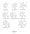
- FIG. 3 shows the chemical structures of Iridium (III) complexes with labels.
- FIG. 4 shows the X-ray crystal structure of Ir(ppy) 2 (CNtBu)(CCPheneatr) (ORTEP view).
- FIG. 5 shows the X-ray crystal structure of Ir(ppz) 2 (CNtBu)(CCPh) (ORTEP view).
- FIG. 6 shows the 1 H NMR (400 MHz, CDCl 3 , ppm) for Ir(ppz) 2 (CNtBu)Cl.
- FIG. 7 shows the 1 H NMR (400 MHz, CD 3 CN, ppm) (A) and the 19 F NMR (376 MHz, CD 3 CN, ppm) (B) for Ir(ppz) 2 (CNtBu)OTf.
- FIG. 8 shows the 1 H NMR (400 MHz, CDCl 3 , ppm) for Ir(ppy) 2 (CNtBu)Cl.
- FIG. 9 shows the 1 H NMR (400 MHz, CD 3 CN, ppm) (A) and the 19 F NMR (376 MHz, CD 3 CN, ppm) for Ir(ppy) 2 (CNtBu)OTf.
- FIG. 10 shows absorption (acetonitrile), excitation and emission (2MeTHF, 77K) spectra of Ir(ppz) 2 (CNtBu)(CCPh).
- FIG. 11 shows the LCMS (C18, acetonitrile:H 2 O, 80:20 to 90:10; ESI+) for Ir(ppz) 2 (CNtBu)(CCPh).
- FIG. 12 shows the absorption (acetonitrile) and emission (toluene, room temperature; 2MeTHF, 77K) spectra of Ir(ppz) 2 (CNtBu)(CCPh).
- FIG. 13 shows the LCMS (C18, acetonitrile:H 2 O, 80:20 to 90:10; ESI+) for Ir(ppy) 2 (CNtBu)(CCPh).
- FIG. 14 shows absorption (acetonitrile), excitation and emission (2MeTHF, 77K) spectra of Ir(ppy) 2 (CNtBu)(CCPheneatr).
- FIG. 15 shows the LCMS (C18, acetonitrile:H 2 O, 80:20 to 90:10; ESI+) of Ir(ppy) 2 (CNtBu)(CCPheneatr).
- FIG. 16 shows the LCMS (C18, acetonitrile:H 2 O, 80:20 to 90:10; ESI+, ⁇ ) for Ir(ppy) 2 (CCPh) 2 Li.
- FIG. 17 shows the UV Absorption (Acetonitrile) of Ir(ppy) 2 (CCPh) 2 Li.
- FIG. 18 shows the absorption (acetonitrile) and emission (2MeTHF, 77K; toluene, room temp.) spectra of Ir(ppz) 2 (CNtBu)(CCPheneatr).
- FIG. 19 shows the LCMS (C8, acetonitrile:H 2 O, 80:20; ESI+) for Ir(ppz) 2 (CNtBu)(CCPheneatr).
- FIG. 20 shows the brightness vs. voltage for devices having the structure ITO/PVK/CBP(Ir complex 8% w/w)/BCP(400 ⁇ )/LiF(10 ⁇ )/Al in which the Ir complex is Ir(ppy) 2 (CNtBu)(CCPheneatr), Ir(ppz) 2 (CNtBu)(CCPheneatr) or Ir(ppy) 3 .
- FIG. 21 shows current density vs. voltage for devices having the structure ITO/PVK/CBP(Ir complex 8% w/w)/BCP(400 ⁇ )/LiF(10 ⁇ )/Al in which the Ir complex is Ir(ppy) 2 (CNtBu)(CCPheneatr), Ir(ppz) 2 (CNtBu)(CCPheneatr) or Ir(ppy) 3 .
- FIG. 22 shows the quantum efficiency vs. current density for devices having the structure ITO/PVK/CBP(Ir complex 8% w/w)/BCP(400 ⁇ )/LiF(10 ⁇ )/Al in which the Ir complex is Ir(ppy) 2 (CNtBu)(CCPheneatr), Ir(ppz) 2 (CNtBu)(CCPheneatr) or Ir(ppy) 3 .
- FIG. 23 shows the electroluminescent emission at 30V for devices having the structure ITO/PVK/CBP(Ir complex 8% w/w)/BCP(400 ⁇ )/LiF(10 ⁇ )/Al in which the Ir complex is Ir(ppy) 2 (CNtBu)(CCPheneatr), Ir(ppz) 2 (CNtBu)(CCPheneatr) or Ir(ppy) 3 .
- an OLED comprises at least one organic layer disposed between and electrically connected to an anode and a cathode.
- the anode injects holes and the cathode injects electrons into the organic layer(s).
- the injected holes and electrons each migrate toward the oppositely charged electrode.
- an “exciton,” which is a localized electron-hole pair having an excited energy state is formed.
- Light is emitted when the exciton relaxes via a photoemissive mechanism.
- the exciton may be localized on an excimer or an exciplex. Non-radiative mechanisms, such as thermal relaxation, may also occur, but are generally considered undesirable.
- the initial OLEDs used emissive molecules that emitted light from their singlet states (“fluorescence”) as disclosed, for example, in U.S. Pat. No. 4,769,292, which is incorporated by reference in its entirety. Fluorescent emission generally occurs in a time frame of less than 10 nanoseconds.
- FIG. 1 shows an organic light emitting device 100 .
- Device 100 may include a substrate 110 , an anode 115 , a hole injection layer 120 , a hole transport layer 125 , an electron blocking layer 130 , an emissive layer 135 , a hole blocking layer 140 , an electron transport layer 145 , an electron injection layer 150 , a protective layer 155 , and a cathode 160 .
- Cathode 160 is a compound cathode having a first conductive layer 162 and a second conductive layer 164 .
- Device 100 may be fabricated by depositing the layers described, in order. The properties and functions of these various layers, as well as example materials, are described in more detail in U.S. Pat. No. 7,279,704 at cols. 6-10, which are incorporated by reference.
- each of these layers are available.
- a flexible and transparent substrate-anode combination is disclosed in U.S. Pat. No. 5,844,363, which is incorporated by reference in its entirety.
- An example of a p-doped hole transport layer is m-MTDATA doped with F.sub.4-TCNQ at a molar ratio of 50:1, as disclosed in U.S. Patent Application Publication No. 2003/0230980, which is incorporated by reference in its entirety.
- Examples of emissive and host materials are disclosed in U.S. Pat. No. 6,303,238 to Thompson et al., which is incorporated by reference in its entirety.
- An example of an n-doped electron transport layer is BPhen doped with Li at a molar ratio of 1:1, as disclosed in U.S. Patent Application Publication No. 2003/0230980, which is incorporated by reference in its entirety.
- the theory and use of blocking layers is described in more detail in U.S. Pat. No. 6,097,147 and U.S. Patent Application Publication No.
- FIG. 2 shows an inverted OLED 200 .
- the device includes a substrate 210 , a cathode 215 , an emissive layer 220 , a hole transport layer 225 , and an anode 230 .
- Device 200 may be fabricated by depositing the layers described, in order. Because the most common OLED configuration has a cathode disposed over the anode, and device 200 has cathode 215 disposed under anode 230 , device 200 may be referred to as an “inverted” OLED. Materials similar to those described with respect to device 100 may be used in the corresponding layers of device 200 .
- FIG. 2 provides one example of how some layers may be omitted from the structure of device 100 .
- FIGS. 1 and 2 The simple layered structure illustrated in FIGS. 1 and 2 is provided by way of non-limiting example, and it is understood that embodiments of the invention may be used in connection with a wide variety of other structures.
- the specific materials and structures described are exemplary in nature, and other materials and structures may be used.
- Functional OLEDs may be achieved by combining the various layers described in different ways, or layers may be omitted entirely, based on design, performance, and cost factors. Other layers not specifically described may also be included. Materials other than those specifically described may be used. Although many of the examples provided herein describe various layers as comprising a single material, it is understood that combinations of materials, such as a mixture of host and dopant, or more generally a mixture, may be used. Also, the layers may have various sublayers.
- hole transport layer 225 transports holes and injects holes into emissive layer 220 , and may be described as a hole transport layer or a hole injection layer.
- an OLED may be described as having an “organic layer” disposed between a cathode and an anode. This organic layer may comprise a single layer, or may further comprise multiple layers of different organic materials as described, for example, with respect to FIGS. 1 and 2 .
- OLEDs comprised of polymeric materials (PLEDs) such as disclosed in U.S. Pat. No. 5,247,190 to Friend et al., which is incorporated by reference in its entirety.
- PLEDs polymeric materials
- OLEDs having a single organic layer may be used.
- OLEDs may be stacked, for example as described in U.S. Pat. No. 5,707,745 to Forrest et al, which is incorporated by reference in its entirety.
- the OLED structure may deviate from the simple layered structure illustrated in FIGS. 1 and 2 .
- the substrate may include an angled reflective surface to improve out-coupling, such as a mesa structure as described in U.S. Pat. No. 6,091,195 to Forrest et al., and/or a pit structure as described in U.S. Pat. No. 5,834,893 to Bulovic et al., which are incorporated by reference in their entireties.
- any of the layers of the various embodiments may be deposited by any suitable method.
- preferred methods include thermal evaporation, ink-jet, such as described in U.S. Pat. Nos. 6,013,982 and 6,087,196, which are incorporated by reference in their entireties, organic vapor phase deposition (OVPD), such as described in U.S. Pat. No. 6,337,102 to Forrest et al., which is incorporated by reference in its entirety, and deposition by organic vapor jet printing (OVJP), such as described in U.S. patent application Ser. No. 10/233,470, which is incorporated by reference in its entirety.
- OVPD organic vapor phase deposition
- OJP organic vapor jet printing
- Other suitable deposition methods include spin coating and other solution based processes.
- Solution based processes are preferably carried out in nitrogen or an inert atmosphere.
- preferred methods include thermal evaporation.
- Preferred patterning methods include deposition through a mask, cold welding such as described in U.S. Pat. Nos. 6,294,398 and 6,468,819, which are incorporated by reference in their entireties, and patterning associated with some of the deposition methods such as ink jet and OVJD. Other methods may also be used.
- the materials to be deposited may be modified to make them compatible with a particular deposition method. For example, substituents such as alkyl and aryl groups, branched or unbranched, and preferably containing at least 3 carbons, may be used in small molecules to enhance their ability to undergo solution processing.
- Substituents having 20 carbons or more may be used, and 3-20 carbons is a preferred range. Materials with asymmetric structures may have better solution processibility than those having symmetric structures, because asymmetric materials may have a lower tendency to recrystallize. Dendrimer substituents may be used to enhance the ability of small molecules to undergo solution processing.
- Devices fabricated in accordance with embodiments of the invention may be incorporated into a wide variety of consumer products, including flat panel displays, computer monitors, televisions, billboards, lights for interior or exterior illumination and/or signaling, heads up displays, fully transparent displays, flexible displays, laser printers, telephones, cell phones, personal digital assistants (PDAs), laptop computers, digital cameras, camcorders, viewfinders, micro-displays, vehicles, a large area wall, theater or stadium screen, or a sign.
- PDAs personal digital assistants
- Various control mechanisms may be used to control devices fabricated in accordance with the present invention, including passive matrix and active matrix. Many of the devices are intended for use in a temperature range comfortable to humans, such as 18 degrees C. to 30 degrees C., and more preferably at room temperature (20-25 degrees C.).
- the materials and structures described herein may have applications in devices other than OLEDs.
- other optoelectronic devices such as organic solar cells and organic photodetectors may employ the materials and structures.
- organic devices such as organic transistors, may employ the materials and structures.
- halo, halogen, alkyl, cycloalkyl, alkenyl, alkynyl, aralkyl, heterocyclic group, aryl, aromatic group, and heteroaryl are known to the art, and are defined in U.S. Pat. No. 7,279,704 at cols. 31-32, which are incorporated herein by reference.
- the devices of the invention have an emissive layer comprising a phosphorescent (triplet-emitting) organometallic material. At least one of the phosphorescent materials in the emissive layer is an Ir(III)cyclometallated alkynyl system.
- the Ir(III)cyclometallated alkynyl complexes comprise at least one cyclometallating ligand.
- the cyclometallating ligand is preferably aromatic, with the bonds between the iridium directly to one or more aromatic rings of which the cyclometallating ligand is comprised.
- the cyclometallating ligand also is preferably bidentate.
- At least one of the bonds to the cyclometallating ligand is a carbon-iridium bond.
- the second bond to the cyclometallating ligand may be through a second carbon-iridium bond or through a bond between a heteroatom and the iridium.
- the heteroatom is nitrogen.
- the iridium is bonded to the cyclometallating ligand through a carbon-iridium bond and a nitrogen-iridium bond.
- the substructure may be represented as:
- X 1 ⁇ X 2 is a substituted or unsubstituted bidentate cyclometallating ligand. It is preferred that X 1 , X 2 , or most preferably both, are a member of an aromatic ring. In preferred embodiments, X 1 and X 2 are independently selected from C and N.
- the bidentate cyclometallating ligand may have the following structure:
- Rings A and B are independently aromatic rings or a fused aromatic rings that bond to the iridium through X 1 and X 2 .
- X 1 and X 2 are independently selected from C and N.
- W is selected from nitrogen and carbon.
- the dotted lines represent optional double bonds.
- the rings can be optionally substituted.
- Optional substituents on the rings include alkyl, alkenyl, alkynyl, aralkyl, CN, CF 3 , NR 2 , NO 2 , OR, halo, and aryl, wherein R is H, alkyl or aryl.
- cyclometallating ligand is a bidentate ligand that is bound to the iridium through a carbon-metal bond and a nitrogen-metal bond to form a cyclometallated ring
- cyclometallating ligand may have the following structure:
- Ring A′ is an aromatic heterocyclic ring or a fused aromatic heterocyclic ring with at least one nitrogen atom that coordinates to iridium. W is selected from carbon or nitrogen.
- Ring B′ is a phenyl group that is bonded to the iridium through a carbon atom, and which may additionally be a member of a fused aromatic ring system.
- the rings can be optionally substituted.
- Optional substituents on the rings include alkyl, alkenyl, alkynyl, aralkyl, CN, CF 3 , NR 2 , NO 2 , OR, halo, and aryl, wherein R is H, alkyl or aryl.
- Representative cyclometallating ligands include:
- cyclometallating ligands may be optionally substituted.
- Optional substituents on the rings include of alkyl, alkenyl, alkynyl, aralkyl, CN, CF 3 , NR 2 , NO 2 , OR, halo, and aryl.
- X is NR, SiR 2 , S and O.
- R is H, alkyl or aryl.
- the Ir(III)cyclometallated alkynyl complexes also comprise at least one bond to an acetylide ligand.
- the acetylide ligand is bonded to the iridium in the Ir(III)cyclometallated alkynyl complex through an acetylide carbon to provide the substructure Ir—C ⁇ C—R 1 .
- the Ir(III)cyclometallated alkynyl complexes may also comprise an ancillary ligand to fill the coordination sphere of the iridium center.
- ancillary because it is believed that they may modify the photoactive properties of the molecule, as opposed to directly contributing to the photoactive properties.
- the definitions of photoactive and ancillary are intended as non-limiting theories.
- the ancillary ligands may be selected from those disclosed in the following references:
- the ancillary ligand is selected to have the formula —C ⁇ N—R 3 ; wherein R 3 is selected from the group consisting of alkyl, cycloalkyl, alkenyl, aryl, aralkyl, and heteroaryl.
- the triplet-emitting material is a compound having the formula I:
- X 1 ⁇ X 2 is a substituted or unsubstituted bidentate cyclometallated aromatic ligand; X 1 and X 2 are independently selected from C and N; Z is an acetylide ligand having the structure: —C ⁇ C—R 1 , —C ⁇ C—(C ⁇ C) x —R 1 , —C ⁇ C-(A-C ⁇ C) y —R 1 , each R 1 is independently selected from the group consisting of H, alkyl, cycloalkyl, alkenyl, cycloalkenyl, aryl, heteroaryl, Si(R 2 ) 3 , M(L) z , and a heterocyclic group, each of which may be substituted or unsubstituted; each x is independently selected from 0-5; each y is independently selected from 0-5; each R 2 is independently selected from H, alkyl, cycloalkyl, alkenyl, cycloalkenyl,
- n is 2, a is 1 and b is 1. In other preferred embodiments, n is 2, a is 2, and b is 0.
- the triplet-emitting material is a compound having the formula II:
- C ⁇ N is a substituted or unsubstituted cyclometallated ligand
- each R 1 is independently selected from the group consisting of H, alkyl, cycloalkyl, alkenyl, cycloalkenyl, aryl, heteroaryl, Si(R 2 ) 3 , M(L) z , and a heterocyclic group, each of which may be substituted or unsubstituted
- each R 2 is independently selected from H, alkyl, cycloalkyl, alkenyl, cycloalkenyl, aryl, heteroaryl, and a heterocyclic group
- M is a metal atom
- L is a mono-, bi- or tridentate ligand
- z is 0-5
- Y is a monodentate ancillary ligand
- Cat is an optional cation the charge of which provides a net neutral charge for formula II.
- the triplet-emitting material is a compound having the formula III:
- C ⁇ N is a substituted or unsubstituted cyclometallated ligand
- R 1a and R 1b are independently selected from the group consisting of H, alkyl, cycloalkyl, alkenyl, cycloalkenyl, aryl, heteroaryl, Si(R 2 ) 3 , M(L) z , and a heterocyclic group, each of which may be substituted or unsubstituted
- each R 2 is independently selected from H, alkyl, cycloalkyl, alkenyl, cycloalkenyl, aryl, heteroaryl, and a heterocyclic group
- M is a metal atom
- L is a mono-, bi- or tridentate ligand
- z is 0-5
- Cat is an optional cation the charge of which provides a net neutral charge for formula III.
- the cation may me selected from any appropriate species having a positive charge, including metal cations (such
- the acetylide ligand (Z) may accommodate a wide variety of substituent groups (designated R 1 , R 1a or R 1b in the above structure).
- R 1 , R 1a or R 1b is independently selected from:
- each X is independently selected from C(R′) d , N(R′) e , S, O, SO, SO 2 and Si(R′) d ; d is 1 or 2; e is 0 or 1; n is 1 to 5; each R is independently selected from H, halo, CN, alkyl, cycloalkyl, alkenyl, aryl, aralkyl, heteroaryl; OR′, NR′ 2 , CO 2 R′, COR′, CONR′ 2 , and Si(R′) 3 ; each R′ is independently selected from H, alkyl, cycloalkyl, alkenyl, aryl, aralkyl, and heteroaryl; M is a metal atom; L is a mono-, bi- or tridentate ligand; and j is 0 to 5.
- each of the above groups depicted as preferred embodiments of R 1 , R 1a or R 1b may be further optionally substituted at any available carbon atom by a substituent selected from halo, CN, alkyl, cycloalkyl, alkenyl, aryl, aralkyl, heteroaryl; OR′, NR′ 2 , CO 2 R′, COR′, CONR′ 2 , and Si(R′) 3 .
- the relative triplet energy of the acetylide ligands and the cyclometallated ligands allow the tuning of the emission of the claimed complexes, such as that if the triplet energy of the acetylides is lower than the cyclometallating ligands, the emission may be driven by the former group.
- the device may include an anode, a cathode, and an organic emissive layer disposed between the anode and the cathode.
- the organic emissive layer may include a host and a phosphorescent dopant.
- the materials described herein as useful for a particular layer in an organic light emitting device may be used in combination with a wide variety of other materials present in the device.
- emissive dopants disclosed herein may be used in conjunction with a wide variety of hosts, transport layers, blocking layers, injection layers, electrodes and other layers that may be present.
- the materials described or referred to below are non-limiting examples of materials that may be useful in combination with the compounds disclosed herein, and one of skill in the art can readily consult the literature to identify other materials that may be useful in combination.
- hole injection materials In addition to and/or in combination with the materials disclosed herein, many hole injection materials, hole transporting materials, host materials, dopant materials, exciton/hole blocking layer materials, electron transporting and electron injecting materials may be used in an OLED.
- Non-limiting examples of the materials that may be used in an OLED in combination with materials disclosed herein are listed in Table 1 below. Table 1 lists non-limiting classes of materials, non-limiting examples of compounds for each class, and references that disclose the materials.
- (C N) 2 Ir (CNtBu)Cl is converted in the corresponding trifluoromethanesulfonate (OTf) by reacting its solution in CH 2 Cl 2 with 1.1 equivalent of AgOTf dissolved in MeOH at room temperature for 1 h. (J. Li et al., Polyhedron, 2004, 23 (2-3), 419-428). The precipitate of AgCl was removed filtering the suspension through celite. The solvent is removed affording the (C N) 2 Ir(CNtBu)OTf.
- the solvent is removed and the crude crystallized from ethyl acetate/hexane or diethylether/hexane.
- the clean product is obtained.
- a solution of fresh LiC ⁇ CPh prepared by reacting 0.046 mL of phenylacetylene (0.42 mmol) and 0.51 mL of 1.5M hexane nBuLi solution (0.34 mmol) in 20 mL of dry THF at ⁇ 78° C. for 0.5 hour, was added drop-wise via cannula to a solution of 200 mg of Ir(ppz) 2 (CNtBu)OTf (0.28 mmol) in 15 mL of dry THF at ⁇ 78° C. The mixture was reacted for 1 h at ⁇ 78° C. and the temperature was raised to RT over 2 hours.
- a solution of fresh LiC ⁇ CPh was prepared by reacting 0.057 mL of phenylacetylene (0.525 mmol) and 0.298 mL of 1.5M nBuLi in hexane solution (0.462 mmol) in 15 mL of dry THF at ⁇ 78° C. for 0.5 hour. The resulting solution was added drop wise via cannula to a solution of 160 mg of Ir(ppy) 2 (CNtBu)OTf (0.22 mmol) in 10 mL of dry THF at ⁇ 78° C. The mixture was reacted for 1 h at ⁇ 78° C. and the temperature was raised to RT over 2 hours. The solvent was removed under reduced pressure and the crude was extracted with diethylether. 67.8 mg of Ir(ppy) 2 (CNtBu)(CCPh) is obtained (45% yield).
- a solution of fresh LiC ⁇ CPhenantrene was prepared by reacting 35 mg of 9-ethinyl-phenantrene (0.173 mmol) and 0.125 mL of 1.5M nBuLi hexane solution (0.173 mmol) in 10 mL of dry THF at ⁇ 78° C. for 0.5 hour. The solution was added drop wise via cannula to a solution of 60 mg of Ir(ppy) 2 (CNtBu)OTf (0.0785 mmol) in 5 mL of dry THF at ⁇ 78° C. The mixture was reacted for 1 h at ⁇ 78° C. and the temperature was raised to RT over 2 hours. The solvent was removed under reduced pressure and the crude was dissolved in diethylether and precipitated with hexane affording 77 mg of Ir(ppy) 2 (CNtBu)(CCPheneatr) (77% yield).
- a solution of fresh LiC ⁇ CPh was prepared by reacting 0.118 mL of phenylacetylene (1.08 mmol) and 0.48 mL of 1.5M hexane nBuLi solution (0.72 mmol) in 50 mL of dry THF at ⁇ 78° C. for 0.5 hour. The solution was added drop wise via cannula to a solution of 150 mg of Ir(ppy) 2 (MeOH) 2 OTf (0.18 mmol) in 10 mL of dry THF at ⁇ 78° C. The mixture was reacted for 1 h at ⁇ 78° C. and the temperature was raised to RT over 2 hours. The solvent was removed under reduced pressure obtaining the Ir(ppy) 2 (CCPh) 2 Li.
- Table 1 provides the photophysical properties at room temperature in toluene (tol) or CH 2 CL 2 (DCM) and at 77K in 2MeTHF (77K). Criteria for the reading of the emissions: peak maxima of the shortest wavelength emission.
- the PVK layer was formed by spin coating on a ITO substrate from a 20 mg/mL chlorobenzene solution at 3000 rpm for 40 seconds and annealed at 150° C. for 1 h.
- the emissive layer was formed using a solution of CBP (with 8% w/w of the Ir complex) spin coated on the PVK layer from a 15 mg/mL chloroform solution (with the proper Ir complex co-dissolved at 8% w/w concentration) at 3000 rpm for 40 sec. No annealing performed was performed for this layer.
- the BCP, LiF and Al were then vacuum deposited in sequence.
- the device data for devices prepared using Ir(ppz) 2 (CNtBu)(CCPhenantr), Ir(ppy) 2 (CNtBu)(CCPhenantr), and, as reference, fac-Ir(ppy) 3 , as the Ir complex are presented in FIGS. 20 to 23 .
Landscapes
- Chemical & Material Sciences (AREA)
- Organic Chemistry (AREA)
- Crystallography & Structural Chemistry (AREA)
- Inorganic Chemistry (AREA)
- Engineering & Computer Science (AREA)
- Materials Engineering (AREA)
- Electroluminescent Light Sources (AREA)
Abstract
Description


wherein:
X1^X2 is a substituted or unsubstituted bidentate cyclometallated aromatic ligand;
X1 and X2 are independently selected from C and N;
Z is an acetylide ligand having the structure:
—C≡C—R1, —C≡C—(C≡C)x—R1, —C≡C-(A-C≡C)y—R1,
each R1 is independently selected from the group consisting of H, alkyl, cycloalkyl, alkenyl, cycloalkenyl, aryl, heteroaryl, Si(R2)3, M(L)z, and a heterocyclic group, each of which may be substituted or unsubstituted;
each x is independently selected from 0-5;
each y is independently selected from 0-5;
each R2 is independently selected from H, alkyl, cycloalkyl, alkenyl, cycloalkenyl, aryl, heteroaryl, and a heterocyclic group;
M is a metal atom;
L is a mono-, bi- or tridentate ligand;
z is 0-5;
A is aryl or heteroaryl;
Y is a monodentate ancillary ligand;
additionally or alternatively, X and Y, two X ligands, and/or two Y ligands may be connected by a bridging moiety;
a is 1, 2, 3, or 4;
b is 0, 1, 2, or 3;
n is 1 or 2;
the sum of a+b+n is 4 or 5; and
Cat is an optional cation the charge of which provides a net neutral charge for formula I.
In the above figure, X1^X2 is a substituted or unsubstituted bidentate cyclometallating ligand. It is preferred that X1, X2, or most preferably both, are a member of an aromatic ring. In preferred embodiments, X1 and X2 are independently selected from C and N.
Rings A and B are independently aromatic rings or a fused aromatic rings that bond to the iridium through X1 and X2. X1 and X2 are independently selected from C and N. W is selected from nitrogen and carbon. The dotted lines represent optional double bonds. The rings can be optionally substituted. Optional substituents on the rings include alkyl, alkenyl, alkynyl, aralkyl, CN, CF3, NR2, NO2, OR, halo, and aryl, wherein R is H, alkyl or aryl.
Ring A′ is an aromatic heterocyclic ring or a fused aromatic heterocyclic ring with at least one nitrogen atom that coordinates to iridium. W is selected from carbon or nitrogen. Ring B′ is a phenyl group that is bonded to the iridium through a carbon atom, and which may additionally be a member of a fused aromatic ring system. The rings can be optionally substituted. Optional substituents on the rings include alkyl, alkenyl, alkynyl, aralkyl, CN, CF3, NR2, NO2, OR, halo, and aryl, wherein R is H, alkyl or aryl.

The above cyclometallating ligands may be optionally substituted. Optional substituents on the rings include of alkyl, alkenyl, alkynyl, aralkyl, CN, CF3, NR2, NO2, OR, halo, and aryl. X is NR, SiR2, S and O. R is H, alkyl or aryl.

wherein:
X1^X2 is a substituted or unsubstituted bidentate cyclometallated aromatic ligand;
X1 and X2 are independently selected from C and N;
Z is an acetylide ligand having the structure:
—C≡C—R1, —C≡C—(C≡C)x—R1, —C≡C-(A-C≡C)y—R1,
each R1 is independently selected from the group consisting of H, alkyl, cycloalkyl, alkenyl, cycloalkenyl, aryl, heteroaryl, Si(R2)3, M(L)z, and a heterocyclic group, each of which may be substituted or unsubstituted;
each x is independently selected from 0-5;
each y is independently selected from 0-5;
each R2 is independently selected from H, alkyl, cycloalkyl, alkenyl, cycloalkenyl, aryl, heteroaryl, and a heterocyclic group;
M is a metal atom;
L is a mono-, bi- or tridentate ligand;
z is 0-5;
A is aryl or heteroaryl;
Y is a monodentate ancillary ligand;
a is 1, 2, 3, or 4;
b is 0, 1, 2, or 3;
n is 1 or 2;
the sum of a+b+n is 4 or 5; and
Cat is an optional cation the charge of which provides a net neutral charge for formula I.

wherein
C^N is a substituted or unsubstituted cyclometallated ligand;
each R1 is independently selected from the group consisting of H, alkyl, cycloalkyl, alkenyl, cycloalkenyl, aryl, heteroaryl, Si(R2)3, M(L)z, and a heterocyclic group, each of which may be substituted or unsubstituted;
each R2 is independently selected from H, alkyl, cycloalkyl, alkenyl, cycloalkenyl, aryl, heteroaryl, and a heterocyclic group;
M is a metal atom;
L is a mono-, bi- or tridentate ligand;
z is 0-5;
Y is a monodentate ancillary ligand; and
Cat is an optional cation the charge of which provides a net neutral charge for formula II.

wherein
C^N is a substituted or unsubstituted cyclometallated ligand;
R1a and R1b are independently selected from the group consisting of
H, alkyl, cycloalkyl, alkenyl, cycloalkenyl, aryl, heteroaryl, Si(R2)3, M(L)z, and a heterocyclic group, each of which may be substituted or unsubstituted;
each R2 is independently selected from H, alkyl, cycloalkyl, alkenyl, cycloalkenyl, aryl, heteroaryl, and a heterocyclic group;
M is a metal atom;
L is a mono-, bi- or tridentate ligand;
z is 0-5;
and
Cat is an optional cation the charge of which provides a net neutral charge for formula III. In each embodiment that may comprise the cation Cat, the cation may me selected from any appropriate species having a positive charge, including metal cations (such as alkali metal cations) and quaternary ammonium cations.


wherein each X is independently selected from C(R′)d, N(R′)e, S, O, SO, SO2 and Si(R′)d;
d is 1 or 2;
e is 0 or 1;
n is 1 to 5;
each R is independently selected from H, halo, CN, alkyl, cycloalkyl, alkenyl, aryl, aralkyl, heteroaryl; OR′, NR′2, CO2R′, COR′, CONR′2, and Si(R′)3;
each R′ is independently selected from H, alkyl, cycloalkyl, alkenyl, aryl, aralkyl, and heteroaryl;
M is a metal atom; L is a mono-, bi- or tridentate ligand; and
j is 0 to 5.
| TABLE 1 | ||
| MATERIAL | EXAMPLES OF MATERIAL | PUBLICATIONS |
| Hole injection materials |
| Phthalocyanine and porphryin compounds |
 |
Appl. Phys. Lett. 69, 2160 (1996) |
| Starburst triarylamines |
 |
J. Lumin. 72-74, 985 (1997) |
| CFx Fluorohydrocarbon polymer |
|
Appl. Phys. Lett. 78, 673 (2001) |
| Conducting polymers (e.g., PEDOT:PSS, polyaniline, polypthiophene) |
 |
Synth. Met. 87, 171 (1997) WO2007002683 |
| Phosphonic acid and sliane SAMs |
|
US20030162053 |
| Triarylamine or polythiophene polymers with conductivity dopants |
 |
EA01725079A1 |
 |
||
 |
||
| Arylamines complexed with metal oxides such as molybdenum and tungsten oxides |
 |
SID Symposium Digest, 37, 923 (2006) WO2009018009 |
| p-type semiconducting organic complexes |
 |
US20020158242 |
| Metal organometallic complexes |
 |
US20060240279 |
| Cross-linkable compounds |
 |
US20080220265 |
| Hole transporting materials |
| Triarylamines (e.g., TPD, α-NPD) |
 |
Appl. Phys. Lett. 51, 913 (1987) |
 |
U.S. Pat. No. 5,061,569 | |
 |
EP650955 | |
 |
J. Mater. Chem. 3, 319 (1993) | |
 |
Appl. Phys. Lett. 90, 183503 (2007) | |
 |
Appl. Phys. Lett. 90, 183503 (2007) | |
| Triaylamine on spirofluorene core |
 |
Synth. Met. 91, 209 (1997) |
| Arylamine carbazole compounds |
 |
Adv. Mater. 6, 677 (1994), US20080124572 |
| Triarylamine with (di)benzothiophene/ (di)benzofuran |
 |
US20070278938, US20080106190 |
| Indolocarbazoles |
 |
Synth. Met. 111, 421 (2000) |
| Isoindole compounds |
 |
Chem. Mater. 15, 3148 (2003) |
| Metal carbene complexes |
 |
US20080018221 |
| Phosphorescent OLED host materials |
| Red hosts |
| Arylcarbazoles |
 |
Appl. Phys. Lett. 78, 1622 (2001) |
| Metal 8-hydroxyquinolates (e.g., Alq3, BAlq) |
 |
Nature 395, 151 (1998) |
 |
US20060202194 | |
 |
WO2005014551 | |
 |
WO2006072002 | |
| Metal phenoxybenzothiazole compounds |
 |
Appl. Phys. Lett. 90, 123509 (2007) |
| Conjugated oligomers and polymers (e.g., polyfluorene) |
 |
Org. Electron. 1, 15 (2000) |
| Aromatic fused rings |
 |
WO2009066779, WO2009066778, WO2009063833, US20090045731, US20090045730, WO2009008311, US20090008605, US20090009065 |
| Zinc complexes |
 |
WO2009062578 |
| Green hosts |
| Arylcarbazoles |
 |
Appl. Phys. Lett. 78, 1622 (2001) |
 |
US20030175553 | |
 |
WO2001039234 | |
| Aryltriphenylene compounds |
 |
US20060280965 |
 |
US20060280965 | |
 |
WO2009021126 | |
| Donor acceptor type molecules |
 |
WO2008056746 |
| Aza-carbazole/DBT/DBF |
 |
JP2008074939 |
| Polymers (e.g., PVK) |
 |
Appl. Phys. Lett. 77, 2280 (2000) |
| Spirofluorene compounds |
 |
WO2004093207 |
| Metal phenoxybenzooxazole compounds |
 |
WO2005089025 |
 |
WO2006132173 | |
 |
JP200511610 | |
| Spirofluorene-carbazole compounds |
 |
JP2007254297 |
 |
JP2007254297 | |
| Indolocabazoles |
 |
WO2007063796 |
 |
WO2007063754 | |
| 5-member ring electron deficient heterocycles (e.g., triazole, oxadiazole) |
 |
J. Appl. Phys. 90, 5048 (2001) |
 |
WO2004107822 | |
| Tetraphenylene complexes |
 |
US20050112407 |
| Metal phenoxypyridine compounds |
 |
WO2005030900 |
| Metal coordination complexes (e.g., Zn, Al with N{circumflex over ( )}N ligands) |
 |
US20040137268, US20040137267 |
| Blue hosts |
| Arylcarbazoles |
 |
Appl. Phys. Lett, 82, 2422 (2003) |
 |
US20070190359 | |
| Dibenzothiophene/ Dibenzofuran-carbazole compounds |
 |
WO2006114966, US20090167162 |
 |
US20090167162 | |
 |
WO2009086028 | |
 |
US20090030202, US20090017330 | |
| Silicon aryl compounds |
 |
US20050238919 |
 |
WO2009003898 | |
| Silicon/Germanium aryl compounds |
 |
EP2034538A |
| Aryl benzoyl ester |
 |
WO2006100298 |
| High triplet metal organometallic complex |
 |
U.S. Pat. No. 7,154,114 |
| Phosphorescent dopants |
| Red dopants |
| Heavy metal porphyrins (e.g., PtOEP) |
 |
Nature 395, 151 (1998) |
| Iridium(III) organometallic complexes |
 |
Appl. Phys. Lett. 78, 1622 (2001) |
 |
US2006835469 | |
 |
US2006835469 | |
 |
US20060202194 | |
 |
US20060202194 | |
 |
US20070087321 | |
 |
US20070087321 | |
 |
Adv. Mater. 19, 739 (2007) | |
 |
WO2009100991 | |
 |
WO2008101842 | |
| Platinum(II) organometallic complexes |
 |
WO2003040257 |
| Osminum(III) complexes |
 |
Chem. Mater. 17, 3532 (2005) |
| Ruthenium(II) complexes |
 |
Adv. Mater. 17, 1059 (2005) |
| Rhenium (I), (II), and (III) complexes |
 |
US20050244673 |
| Green dopants |
| Iridium(III) organometallic complexes |
 |
Inorg. Chem. 40, 1704 (2001) |
 |
US20020034656 | |
 |
U.S. Pat. No. 7,332,232 | |
 |
US20090108737 | |
 |
US20090039776 | |
 |
U.S. Pat. No. 6,921,915 | |
 |
U.S. Pat. No. 6,687,266 | |
 |
Chem. Mater. 16, 2480 (2004) | |
 |
US20070190359 | |
 |
US 20060008670 JP2007123392 | |
 |
Adv. Mater. 16, 2003 (2004) | |
 |
Angew. Chem. Int. Ed. 2006, 45, 7800 | |
 |
WO2009050290 | |
 |
US20090165846 | |
 |
US20080015355 | |
| Monomer for polymeric metal organometallic compounds |
 |
U.S. Pat. No. 7,250,226, U.S. Pat. No. 7,396,598 |
| Pt(II) organometallic complexes, including polydentated ligands |
 |
Appl. Phys. Lett. 86, 153505 (2005) |
 |
Appl. Phys. Lett. 86, 153505 (2005) | |
 |
Chem. Lett. 34, 592 (2005) | |
 |
WO2002015645 | |
 |
US20060263635 | |
| Cu complexes |
 |
WO2009000673 |
| Gold complexes |
 |
Chem. Commun. 2906 (2005) |
| Rhenium(III) complexes |
 |
Inorg. Chem. 42, 1248 (2003) |
| Deuterated organometallic complexes |
 |
US20030138657 |
| Organometallic complexes with two or more metal centers |
 |
US20030152802 |
 |
U.S. Pat. No. 7,090,928 | |
| Blue dopants |
| Iridium(III) organometallic complexes |
 |
WO2002002714 |
 |
WO2006009024 | |
 |
US20060251923 | |
 |
U.S. Pat. No. 7,393,599, WO2006056418, US20050260441, WO2005019373 | |
 |
U.S. Pat. No. 7,534,505 | |
 |
U.S. Pat. No. 7,445,855 | |
 |
US20070190359, US20080297033 | |
 |
U.S. Pat. No. 7,338,722 | |
 |
US20020134984 | |
 |
Angew. Chem. Int. Ed. 47, 1 (2008) | |
 |
Chem. Mater. 18, 5119 (2006) | |
 |
Inorg. Chem. 46, 4308 (2007) | |
 |
WO2005123873 | |
 |
WO2005123873 | |
 |
WO2007004380 | |
 |
WO2006082742 | |
| Osmium(II) complexes |
 |
U.S. Pat. No. 7,279,704 |
 |
Organometallics 23, 3745 (2004) | |
| Gold complexes |
|
Appl. Phys. Lett. 74, 1361 (1999) |
| Platinum(II) complexes |
 |
WO2006098120, WO2006103874 |
| Exciton/hole blocking layer materials |
| Bathocuprine compounds (e.g., BCP, BPhen) |
 |
Appl. Phys. Lett. 75, 4 (1999) |
 |
Appl. Phys. Lett. 79, 449 (2001) | |
| Metal 8-hydroxyquinolates (e.g., BAlq) |
 |
Appl. Phys. Lett. 81, 162 (2002) |
| 5-member ring electron deficient heterocycles such as triazole, oxadiazole, imidazole, benzoimidazole |
 |
Appl. Phys. Lett. 81, 162 (2002) |
| Triphenylene compounds |
 |
US20050025993 |
| Fluorinated aromatic compounds |
 |
Appl. Phys. Lett. 79, 156 (2001) |
| Phenothiazine-S-oxide |
 |
WO2008132085 |
| Electron transporting materials |
| Anthracene- benzoimidazole compounds |
 |
WO2003060956 |
 |
US20090179554 | |
| Aza triphenylene derivatives |
 |
US20090115316 |
| Anthracene-benzothiazole compounds |
 |
Appl. Phys. Lett. 89, 063504 (2006) |
| Metal 8-hydroxyquinolates (e.g., Alq3, Zrq4) |
 |
Appl. Phys. Lett. 51, 913 (1987) U.S. Pat. No. 7,230,107 |
| Metal hydroxybenoquinolates |
 |
Chem. Lett. 5, 905 (1993) |
| Bathocuprine compounds such as BCP, BPhen, etc |
 |
Appl. Phys. Lett. 91, 263503 (2007) |
 |
Appl. Phys. Lett. 79, 449 (2001) | |
| 5-member ring electron deficient heterocycles (e.g.,triazole, oxadiazole, imidazole, benzoimidazole) |
 |
Appl. Phys. Lett. 74, 865 (1999) |
 |
Appl. Phys. Lett. 55, 1489 (1989) | |
 |
Jpn. J. Apply. Phys. 32, L917 (1993) | |
| Silole compounds |
 |
Org. Electron. 4, 113 (2003) |
| Arylborane compounds |
 |
J. Am. Chem. Soc. 120, 9714 (1998) |
| Fluorinated aromatic compounds |
 |
J. Am. Chem. Soc. 122, 1832 (2000) |
| Fullerene (e.g., C60) |
 |
US20090101870 |
| Triazine complexes |
 |
US20040036077 |
| Zn (N{circumflex over ( )}N) complexes |
 |
U.S. Pat. No. 6,528,187 |


| TABLE 2 | |||
| | Emission | 77K | |
| λ | λ | ||||
| Compound | (nm) | Φ PL | τ μs | (nm) | τ μs |
| Ir(ppz)2(CNtBu) | — | — | — | 420 | 1460 |
| (CCPh) | |||||
| Ir(ppz)2(CNtBu) | 548 | 0.07(tol) | 442 | 531 | 1758 |
| (CCPhenantr) | |||||
| Ir(ppy)2(CNtBu) | 472 | 0.26(tol) | 0.81(70%) | 458 | 4.3(64%) |
| (CCPh) | 1.92(30%) | 9.06(36%)a | |||
| 4.77b | |||||
| Ir(ppy)2(CNtBu) | 470 | 0.07(DCM) | 0.52 and | 530 | 1515 |
| (CCPhenantr) | 156 | ||||
| alifetime @ 500 nm; | |||||
| blifetime @ 460 nm; | |||||
-
- ITO/PVK/CBP(Ir complex 8% w/w)/BCP(400 Å)/LiF(10 Å)/Al
Claims (3)


Priority Applications (2)
| Application Number | Priority Date | Filing Date | Title |
|---|---|---|---|
| US13/161,296 US8822042B2 (en) | 2010-06-28 | 2011-06-15 | Luminescent cyclometallated iridium(III) complexes having acetylide ligands |
| US14/450,708 US20150076470A1 (en) | 2010-06-28 | 2014-08-04 | Luminescent Cyclometallated Iridium (III) Complexes Having Acetylide Ligands |
Applications Claiming Priority (2)
| Application Number | Priority Date | Filing Date | Title |
|---|---|---|---|
| US35911810P | 2010-06-28 | 2010-06-28 | |
| US13/161,296 US8822042B2 (en) | 2010-06-28 | 2011-06-15 | Luminescent cyclometallated iridium(III) complexes having acetylide ligands |
Related Child Applications (1)
| Application Number | Title | Priority Date | Filing Date |
|---|---|---|---|
| US14/450,708 Continuation US20150076470A1 (en) | 2010-06-28 | 2014-08-04 | Luminescent Cyclometallated Iridium (III) Complexes Having Acetylide Ligands |
Publications (2)
| Publication Number | Publication Date |
|---|---|
| US20120007061A1 US20120007061A1 (en) | 2012-01-12 |
| US8822042B2 true US8822042B2 (en) | 2014-09-02 |
Family
ID=45437943
Family Applications (2)
| Application Number | Title | Priority Date | Filing Date |
|---|---|---|---|
| US13/161,296 Active 2032-10-27 US8822042B2 (en) | 2010-06-28 | 2011-06-15 | Luminescent cyclometallated iridium(III) complexes having acetylide ligands |
| US14/450,708 Abandoned US20150076470A1 (en) | 2010-06-28 | 2014-08-04 | Luminescent Cyclometallated Iridium (III) Complexes Having Acetylide Ligands |
Family Applications After (1)
| Application Number | Title | Priority Date | Filing Date |
|---|---|---|---|
| US14/450,708 Abandoned US20150076470A1 (en) | 2010-06-28 | 2014-08-04 | Luminescent Cyclometallated Iridium (III) Complexes Having Acetylide Ligands |
Country Status (1)
| Country | Link |
|---|---|
| US (2) | US8822042B2 (en) |
Cited By (1)
| Publication number | Priority date | Publication date | Assignee | Title |
|---|---|---|---|---|
| US9478758B1 (en) * | 2015-05-08 | 2016-10-25 | Universal Display Corporation | Organic electroluminescent materials and devices |
Families Citing this family (4)
| Publication number | Priority date | Publication date | Assignee | Title |
|---|---|---|---|---|
| DE102013225682A1 (en) * | 2013-12-12 | 2015-06-18 | Friedrich-Alexander-Universität Erlangen-Nürnberg | Metal ion adducts of neutral phosphorescent emitters for use in light emitting organic optoelectronic devices |
| US10497893B2 (en) * | 2015-04-15 | 2019-12-03 | Lg Electronics Inc. | Method for doping graphene, method for manufacturing graphene composite electrode, and graphene structure comprising same |
| US10672998B2 (en) | 2017-03-23 | 2020-06-02 | Universal Display Corporation | Organic electroluminescent materials and devices |
| CN108948093B (en) * | 2018-07-12 | 2020-10-02 | 南京邮电大学 | Phosphorescent metal iridium complex with singlet oxygen detection effect and preparation method and application thereof |
Citations (3)
| Publication number | Priority date | Publication date | Assignee | Title |
|---|---|---|---|---|
| US20050112406A1 (en) * | 2003-11-06 | 2005-05-26 | Eun-Sil Han | Organometallic complexes and organic electroluminescence device using the same |
| US20060115675A1 (en) * | 2004-11-10 | 2006-06-01 | Idemitsu Kosan Co., Ltd. | Metal-complex compound ands organic electroluminescence device using the compound |
| US20070141398A1 (en) * | 2005-12-15 | 2007-06-21 | Idemitsu Kosan Co., Ltd. | Metal complex compound and organic electroluminescence device using the compound |
-
2011
- 2011-06-15 US US13/161,296 patent/US8822042B2/en active Active
-
2014
- 2014-08-04 US US14/450,708 patent/US20150076470A1/en not_active Abandoned
Patent Citations (3)
| Publication number | Priority date | Publication date | Assignee | Title |
|---|---|---|---|---|
| US20050112406A1 (en) * | 2003-11-06 | 2005-05-26 | Eun-Sil Han | Organometallic complexes and organic electroluminescence device using the same |
| US20060115675A1 (en) * | 2004-11-10 | 2006-06-01 | Idemitsu Kosan Co., Ltd. | Metal-complex compound ands organic electroluminescence device using the compound |
| US20070141398A1 (en) * | 2005-12-15 | 2007-06-21 | Idemitsu Kosan Co., Ltd. | Metal complex compound and organic electroluminescence device using the compound |
Non-Patent Citations (1)
| Title |
|---|
| Liu et al. "Theoretical studies on structures and spectroscopic properties of a series of novel mixed-ligand Ir(III) complexes [Ir(Mebib)(ppy)X]" Dalton Trans. 2007. pp. 1922-1928. * |
Cited By (1)
| Publication number | Priority date | Publication date | Assignee | Title |
|---|---|---|---|---|
| US9478758B1 (en) * | 2015-05-08 | 2016-10-25 | Universal Display Corporation | Organic electroluminescent materials and devices |
Also Published As
| Publication number | Publication date |
|---|---|
| US20150076470A1 (en) | 2015-03-19 |
| US20120007061A1 (en) | 2012-01-12 |
Similar Documents
| Publication | Publication Date | Title |
|---|---|---|
| US12295199B2 (en) | Phosphorescence-sensitized delayed fluorescence light emitting system | |
| US11600791B2 (en) | Organic electroluminescent materials and devices | |
| US11380854B2 (en) | Heteroleptic iridium complexes as dopants | |
| US8367223B2 (en) | Heteroleptic phosphorescent emitters | |
| US9175211B2 (en) | Phosphorescent materials | |
| US9670404B2 (en) | Organic electroluminescent materials and devices | |
| US10008678B2 (en) | Organic electroluminescent materials and devices | |
| US8269317B2 (en) | Phosphorescent materials | |
| US9193745B2 (en) | Heteroleptic iridium complex | |
| US9773986B2 (en) | Copper(I)-carbene complexes and organic electroluminescent devices | |
| US8492006B2 (en) | Germanium-containing red emitter materials for organic light emitting diode | |
| US10033000B2 (en) | Organic electroluminescent materials and devices | |
| US9217004B2 (en) | Organic light emitting materials | |
| US20170047531A1 (en) | Organic electroluminescent materials and devices | |
| US20130082245A1 (en) | Tetradentate platinum complexes | |
| US20150076470A1 (en) | Luminescent Cyclometallated Iridium (III) Complexes Having Acetylide Ligands | |
| US10147892B2 (en) | Organic electroluminescent materials and devices | |
| US12408242B2 (en) | Heteroleptic iridium complexes as dopants |
Legal Events
| Date | Code | Title | Description |
|---|---|---|---|
| AS | Assignment |
Owner name: THE UNIVERSITY OF SOUTHERN CALIFORNIA, CALIFORNIA Free format text: ASSIGNMENT OF ASSIGNORS INTEREST;ASSIGNORS:THOMPSON, MARK E.;BOSSI, ALBERTO;DJUROVICH, PETER;SIGNING DATES FROM 20110622 TO 20110623;REEL/FRAME:026974/0498 |
|
| STCF | Information on status: patent grant |
Free format text: PATENTED CASE |
|
| MAFP | Maintenance fee payment |
Free format text: PAYMENT OF MAINTENANCE FEE, 4TH YEAR, LARGE ENTITY (ORIGINAL EVENT CODE: M1551) Year of fee payment: 4 |
|
| MAFP | Maintenance fee payment |
Free format text: PAYMENT OF MAINTENANCE FEE, 8TH YEAR, LARGE ENTITY (ORIGINAL EVENT CODE: M1552); ENTITY STATUS OF PATENT OWNER: LARGE ENTITY Year of fee payment: 8 |