US8819933B2 - Method for forming a current distribution structure - Google Patents
Method for forming a current distribution structure Download PDFInfo
- Publication number
- US8819933B2 US8819933B2 US12/957,431 US95743110A US8819933B2 US 8819933 B2 US8819933 B2 US 8819933B2 US 95743110 A US95743110 A US 95743110A US 8819933 B2 US8819933 B2 US 8819933B2
- Authority
- US
- United States
- Prior art keywords
- conductive pad
- electrically conductive
- wire trace
- wire
- electrically
- Prior art date
- Legal status (The legal status is an assumption and is not a legal conclusion. Google has not performed a legal analysis and makes no representation as to the accuracy of the status listed.)
- Expired - Fee Related, expires
Links
Images


Classifications
-
- H—ELECTRICITY
- H10—SEMICONDUCTOR DEVICES; ELECTRIC SOLID-STATE DEVICES NOT OTHERWISE PROVIDED FOR
- H10W—GENERIC PACKAGES, INTERCONNECTIONS, CONNECTORS OR OTHER CONSTRUCTIONAL DETAILS OF DEVICES COVERED BY CLASS H10
- H10W72/00—Interconnections or connectors in packages
- H10W72/20—Bump connectors, e.g. solder bumps or copper pillars; Dummy bumps; Thermal bumps
-
- H—ELECTRICITY
- H05—ELECTRIC TECHNIQUES NOT OTHERWISE PROVIDED FOR
- H05K—PRINTED CIRCUITS; CASINGS OR CONSTRUCTIONAL DETAILS OF ELECTRIC APPARATUS; MANUFACTURE OF ASSEMBLAGES OF ELECTRICAL COMPONENTS
- H05K1/00—Printed circuits
- H05K1/02—Details
- H05K1/0213—Electrical arrangements not otherwise provided for
- H05K1/0263—High current adaptations, e.g. printed high current conductors or using auxiliary non-printed means; Fine and coarse circuit patterns on one circuit board
- H05K1/0265—High current adaptations, e.g. printed high current conductors or using auxiliary non-printed means; Fine and coarse circuit patterns on one circuit board characterized by the lay-out of or details of the printed conductors, e.g. reinforced conductors, redundant conductors, conductors having different cross-sections
-
- H—ELECTRICITY
- H05—ELECTRIC TECHNIQUES NOT OTHERWISE PROVIDED FOR
- H05K—PRINTED CIRCUITS; CASINGS OR CONSTRUCTIONAL DETAILS OF ELECTRIC APPARATUS; MANUFACTURE OF ASSEMBLAGES OF ELECTRICAL COMPONENTS
- H05K1/00—Printed circuits
- H05K1/02—Details
- H05K1/11—Printed elements for providing electric connections to or between printed circuits
- H05K1/111—Pads for surface mounting, e.g. lay-out
-
- H—ELECTRICITY
- H10—SEMICONDUCTOR DEVICES; ELECTRIC SOLID-STATE DEVICES NOT OTHERWISE PROVIDED FOR
- H10W—GENERIC PACKAGES, INTERCONNECTIONS, CONNECTORS OR OTHER CONSTRUCTIONAL DETAILS OF DEVICES COVERED BY CLASS H10
- H10W20/00—Interconnections in chips, wafers or substrates
- H10W20/40—Interconnections external to wafers or substrates, e.g. back-end-of-line [BEOL] metallisations or vias connecting to gate electrodes
- H10W20/41—Interconnections external to wafers or substrates, e.g. back-end-of-line [BEOL] metallisations or vias connecting to gate electrodes characterised by their conductive parts
- H10W20/43—Layouts of interconnections
-
- H—ELECTRICITY
- H10—SEMICONDUCTOR DEVICES; ELECTRIC SOLID-STATE DEVICES NOT OTHERWISE PROVIDED FOR
- H10W—GENERIC PACKAGES, INTERCONNECTIONS, CONNECTORS OR OTHER CONSTRUCTIONAL DETAILS OF DEVICES COVERED BY CLASS H10
- H10W70/00—Package substrates; Interposers; Redistribution layers [RDL]
- H10W70/60—Insulating or insulated package substrates; Interposers; Redistribution layers
- H10W70/62—Insulating or insulated package substrates; Interposers; Redistribution layers characterised by their interconnections
- H10W70/65—Shapes or dispositions of interconnections
-
- H—ELECTRICITY
- H05—ELECTRIC TECHNIQUES NOT OTHERWISE PROVIDED FOR
- H05K—PRINTED CIRCUITS; CASINGS OR CONSTRUCTIONAL DETAILS OF ELECTRIC APPARATUS; MANUFACTURE OF ASSEMBLAGES OF ELECTRICAL COMPONENTS
- H05K1/00—Printed circuits
- H05K1/02—Details
- H05K1/11—Printed elements for providing electric connections to or between printed circuits
- H05K1/111—Pads for surface mounting, e.g. lay-out
- H05K1/112—Pads for surface mounting, e.g. lay-out directly combined with via connections
-
- H—ELECTRICITY
- H05—ELECTRIC TECHNIQUES NOT OTHERWISE PROVIDED FOR
- H05K—PRINTED CIRCUITS; CASINGS OR CONSTRUCTIONAL DETAILS OF ELECTRIC APPARATUS; MANUFACTURE OF ASSEMBLAGES OF ELECTRICAL COMPONENTS
- H05K2201/00—Indexing scheme relating to printed circuits covered by H05K1/00
- H05K2201/07—Electric details
- H05K2201/0753—Insulation
- H05K2201/0769—Anti metal-migration, e.g. avoiding tin whisker growth
-
- H—ELECTRICITY
- H05—ELECTRIC TECHNIQUES NOT OTHERWISE PROVIDED FOR
- H05K—PRINTED CIRCUITS; CASINGS OR CONSTRUCTIONAL DETAILS OF ELECTRIC APPARATUS; MANUFACTURE OF ASSEMBLAGES OF ELECTRICAL COMPONENTS
- H05K2201/00—Indexing scheme relating to printed circuits covered by H05K1/00
- H05K2201/09—Shape and layout
- H05K2201/09209—Shape and layout details of conductors
- H05K2201/09372—Pads and lands
- H05K2201/09436—Pads or lands on permanent coating which covers the other conductors
-
- H—ELECTRICITY
- H05—ELECTRIC TECHNIQUES NOT OTHERWISE PROVIDED FOR
- H05K—PRINTED CIRCUITS; CASINGS OR CONSTRUCTIONAL DETAILS OF ELECTRIC APPARATUS; MANUFACTURE OF ASSEMBLAGES OF ELECTRICAL COMPONENTS
- H05K2201/00—Indexing scheme relating to printed circuits covered by H05K1/00
- H05K2201/09—Shape and layout
- H05K2201/09209—Shape and layout details of conductors
- H05K2201/095—Conductive through-holes or vias
- H05K2201/09509—Blind vias, i.e. vias having one side closed
-
- H—ELECTRICITY
- H05—ELECTRIC TECHNIQUES NOT OTHERWISE PROVIDED FOR
- H05K—PRINTED CIRCUITS; CASINGS OR CONSTRUCTIONAL DETAILS OF ELECTRIC APPARATUS; MANUFACTURE OF ASSEMBLAGES OF ELECTRICAL COMPONENTS
- H05K2201/00—Indexing scheme relating to printed circuits covered by H05K1/00
- H05K2201/09—Shape and layout
- H05K2201/09209—Shape and layout details of conductors
- H05K2201/09654—Shape and layout details of conductors covering at least two types of conductors provided for in H05K2201/09218 - H05K2201/095
- H05K2201/0979—Redundant conductors or connections, i.e. more than one current path between two points
-
- H—ELECTRICITY
- H10—SEMICONDUCTOR DEVICES; ELECTRIC SOLID-STATE DEVICES NOT OTHERWISE PROVIDED FOR
- H10W—GENERIC PACKAGES, INTERCONNECTIONS, CONNECTORS OR OTHER CONSTRUCTIONAL DETAILS OF DEVICES COVERED BY CLASS H10
- H10W72/00—Interconnections or connectors in packages
- H10W72/071—Connecting or disconnecting
- H10W72/072—Connecting or disconnecting of bump connectors
- H10W72/07251—Connecting or disconnecting of bump connectors characterised by changes in properties of the bump connectors during connecting
-
- H—ELECTRICITY
- H10—SEMICONDUCTOR DEVICES; ELECTRIC SOLID-STATE DEVICES NOT OTHERWISE PROVIDED FOR
- H10W—GENERIC PACKAGES, INTERCONNECTIONS, CONNECTORS OR OTHER CONSTRUCTIONAL DETAILS OF DEVICES COVERED BY CLASS H10
- H10W72/00—Interconnections or connectors in packages
- H10W72/20—Bump connectors, e.g. solder bumps or copper pillars; Dummy bumps; Thermal bumps
- H10W72/241—Dispositions, e.g. layouts
- H10W72/242—Dispositions, e.g. layouts relative to the surface, e.g. recessed, protruding
-
- H—ELECTRICITY
- H10—SEMICONDUCTOR DEVICES; ELECTRIC SOLID-STATE DEVICES NOT OTHERWISE PROVIDED FOR
- H10W—GENERIC PACKAGES, INTERCONNECTIONS, CONNECTORS OR OTHER CONSTRUCTIONAL DETAILS OF DEVICES COVERED BY CLASS H10
- H10W72/00—Interconnections or connectors in packages
- H10W72/20—Bump connectors, e.g. solder bumps or copper pillars; Dummy bumps; Thermal bumps
- H10W72/251—Materials
- H10W72/252—Materials comprising solid metals or solid metalloids, e.g. PbSn, Ag or Cu
-
- H—ELECTRICITY
- H10—SEMICONDUCTOR DEVICES; ELECTRIC SOLID-STATE DEVICES NOT OTHERWISE PROVIDED FOR
- H10W—GENERIC PACKAGES, INTERCONNECTIONS, CONNECTORS OR OTHER CONSTRUCTIONAL DETAILS OF DEVICES COVERED BY CLASS H10
- H10W72/00—Interconnections or connectors in packages
- H10W72/20—Bump connectors, e.g. solder bumps or copper pillars; Dummy bumps; Thermal bumps
- H10W72/29—Bond pads specially adapted therefor
-
- H—ELECTRICITY
- H10—SEMICONDUCTOR DEVICES; ELECTRIC SOLID-STATE DEVICES NOT OTHERWISE PROVIDED FOR
- H10W—GENERIC PACKAGES, INTERCONNECTIONS, CONNECTORS OR OTHER CONSTRUCTIONAL DETAILS OF DEVICES COVERED BY CLASS H10
- H10W72/00—Interconnections or connectors in packages
- H10W72/90—Bond pads, in general
- H10W72/921—Structures or relative sizes of bond pads
- H10W72/923—Bond pads having multiple stacked layers
-
- H—ELECTRICITY
- H10—SEMICONDUCTOR DEVICES; ELECTRIC SOLID-STATE DEVICES NOT OTHERWISE PROVIDED FOR
- H10W—GENERIC PACKAGES, INTERCONNECTIONS, CONNECTORS OR OTHER CONSTRUCTIONAL DETAILS OF DEVICES COVERED BY CLASS H10
- H10W72/00—Interconnections or connectors in packages
- H10W72/90—Bond pads, in general
- H10W72/931—Shapes of bond pads
- H10W72/934—Cross-sectional shape, i.e. in side view
-
- H—ELECTRICITY
- H10—SEMICONDUCTOR DEVICES; ELECTRIC SOLID-STATE DEVICES NOT OTHERWISE PROVIDED FOR
- H10W—GENERIC PACKAGES, INTERCONNECTIONS, CONNECTORS OR OTHER CONSTRUCTIONAL DETAILS OF DEVICES COVERED BY CLASS H10
- H10W72/00—Interconnections or connectors in packages
- H10W72/90—Bond pads, in general
- H10W72/941—Dispositions of bond pads
- H10W72/9415—Dispositions of bond pads relative to the surface, e.g. recessed, protruding
-
- Y—GENERAL TAGGING OF NEW TECHNOLOGICAL DEVELOPMENTS; GENERAL TAGGING OF CROSS-SECTIONAL TECHNOLOGIES SPANNING OVER SEVERAL SECTIONS OF THE IPC; TECHNICAL SUBJECTS COVERED BY FORMER USPC CROSS-REFERENCE ART COLLECTIONS [XRACs] AND DIGESTS
- Y02—TECHNOLOGIES OR APPLICATIONS FOR MITIGATION OR ADAPTATION AGAINST CLIMATE CHANGE
- Y02P—CLIMATE CHANGE MITIGATION TECHNOLOGIES IN THE PRODUCTION OR PROCESSING OF GOODS
- Y02P70/00—Climate change mitigation technologies in the production process for final industrial or consumer products
- Y02P70/50—Manufacturing or production processes characterised by the final manufactured product
-
- Y—GENERAL TAGGING OF NEW TECHNOLOGICAL DEVELOPMENTS; GENERAL TAGGING OF CROSS-SECTIONAL TECHNOLOGIES SPANNING OVER SEVERAL SECTIONS OF THE IPC; TECHNICAL SUBJECTS COVERED BY FORMER USPC CROSS-REFERENCE ART COLLECTIONS [XRACs] AND DIGESTS
- Y10—TECHNICAL SUBJECTS COVERED BY FORMER USPC
- Y10T—TECHNICAL SUBJECTS COVERED BY FORMER US CLASSIFICATION
- Y10T29/00—Metal working
- Y10T29/49—Method of mechanical manufacture
- Y10T29/49002—Electrical device making
- Y10T29/49117—Conductor or circuit manufacturing
- Y10T29/49124—On flat or curved insulated base, e.g., printed circuit, etc.
- Y10T29/4913—Assembling to base an electrical component, e.g., capacitor, etc.
- Y10T29/49144—Assembling to base an electrical component, e.g., capacitor, etc. by metal fusion
-
- Y—GENERAL TAGGING OF NEW TECHNOLOGICAL DEVELOPMENTS; GENERAL TAGGING OF CROSS-SECTIONAL TECHNOLOGIES SPANNING OVER SEVERAL SECTIONS OF THE IPC; TECHNICAL SUBJECTS COVERED BY FORMER USPC CROSS-REFERENCE ART COLLECTIONS [XRACs] AND DIGESTS
- Y10—TECHNICAL SUBJECTS COVERED BY FORMER USPC
- Y10T—TECHNICAL SUBJECTS COVERED BY FORMER US CLASSIFICATION
- Y10T29/00—Metal working
- Y10T29/49—Method of mechanical manufacture
- Y10T29/49002—Electrical device making
- Y10T29/49117—Conductor or circuit manufacturing
- Y10T29/49124—On flat or curved insulated base, e.g., printed circuit, etc.
- Y10T29/49147—Assembling terminal to base
- Y10T29/49149—Assembling terminal to base by metal fusion bonding
-
- Y—GENERAL TAGGING OF NEW TECHNOLOGICAL DEVELOPMENTS; GENERAL TAGGING OF CROSS-SECTIONAL TECHNOLOGIES SPANNING OVER SEVERAL SECTIONS OF THE IPC; TECHNICAL SUBJECTS COVERED BY FORMER USPC CROSS-REFERENCE ART COLLECTIONS [XRACs] AND DIGESTS
- Y10—TECHNICAL SUBJECTS COVERED BY FORMER USPC
- Y10T—TECHNICAL SUBJECTS COVERED BY FORMER US CLASSIFICATION
- Y10T29/00—Metal working
- Y10T29/49—Method of mechanical manufacture
- Y10T29/49002—Electrical device making
- Y10T29/49117—Conductor or circuit manufacturing
- Y10T29/49124—On flat or curved insulated base, e.g., printed circuit, etc.
- Y10T29/49155—Manufacturing circuit on or in base
-
- Y—GENERAL TAGGING OF NEW TECHNOLOGICAL DEVELOPMENTS; GENERAL TAGGING OF CROSS-SECTIONAL TECHNOLOGIES SPANNING OVER SEVERAL SECTIONS OF THE IPC; TECHNICAL SUBJECTS COVERED BY FORMER USPC CROSS-REFERENCE ART COLLECTIONS [XRACs] AND DIGESTS
- Y10—TECHNICAL SUBJECTS COVERED BY FORMER USPC
- Y10T—TECHNICAL SUBJECTS COVERED BY FORMER US CLASSIFICATION
- Y10T29/00—Metal working
- Y10T29/49—Method of mechanical manufacture
- Y10T29/49002—Electrical device making
- Y10T29/49117—Conductor or circuit manufacturing
- Y10T29/49174—Assembling terminal to elongated conductor
- Y10T29/49179—Assembling terminal to elongated conductor by metal fusion bonding
Definitions
- the present invention relates to forming an electrical structure for distributing a current signal.
- Structures formed on a substrate typically do not comprise the ability to route signals to various portions of the structures. Accordingly, there exists a need in the art to overcome at least one of the deficiencies and limitations described herein above.
- the present invention provides an electrical structure comprising:
- said first substrate comprises a first electrically conductive pad and a first plurality of wire traces electrically connected to said first electrically conductive pad, wherein said first electrically conductive pad is electrically and mechanically connected to said first interconnect structure, wherein said first plurality of wire traces comprises a first wire trace, a second wire trace, a third wire trace, and a fourth wire trace, wherein said first wire trace is electrically connected to a first side of said first electrically conductive pad, wherein said second wire trace is electrically connected to said first side of said first electrically conductive pad, wherein said third wire trace is electrically connected to a second side of said first electrically conductive pad, wherein said fourth wire trace is electrically connected to a third side of said first electrically conductive pad, wherein said first side of said first electrically conductive pad is connected to said second side of said first electrically conductive pad at a first non-zero degree angle, wherein said first side of said first electrically conductive pad is connected to said third side of said first
- the present invention provides a method for forming an electrical structure comprising:
- first plurality of wire traces are electrically connected to said first electrically conductive pad
- said first plurality of wire traces comprises a first wire trace, a second wire trace, a third wire trace, and a fourth wire trace
- said first wire trace is electrically connected to a first side of said first electrically conductive pad
- said second wire trace is electrically connected to said first side of said first electrically conductive pad
- said third wire trace is electrically connected to a second side of said first electrically conductive pad
- said fourth wire trace is electrically connected to a third side of said first electrically conductive pad
- said first side of said first electrically conductive pad is connected to said second side of said first electrically conductive pad at a first non-zero degree angle
- said first side of said first electrically conductive pad is connected to said third side of said first electrically conductive pad at a second non-zero degree angle
- said first plurality of wire traces is electrically connected to said third side of said first electrically conductive pad at a second non-zero degree
- first interconnect structure electrically and mechanically connected to said first electrically conductive pad, wherein said first interconnect structure is configured to electrically connect said first electrically conductive pad to a second electrically conductive pad on a second substrate.
- the present invention advantageously provides a simple structure and associated method for routing signals to various portions of structures.
- FIG. 1 illustrates a top view of an electrical structure, in accordance with embodiments of the present invention.
- FIG. 2 illustrates a cross sectional view of the electrical structure of FIG. 1 , in accordance with embodiments of the present invention.
- FIG. 3 depicts a first alternative to FIG. 1 , in accordance with embodiments of the present invention
- FIG. 4 depicts a second alternative to FIG. 1 , in accordance with embodiments of the present invention.
- FIG. 5 depicts a first alternative to FIG. 3 and FIG. 4 , in accordance with embodiments of the present invention.
- FIG. 6 depicts a third alternative to FIG. 1 , in accordance with embodiments of the present invention
- FIG. 7 depicts a first alternative to FIG. 6 , in accordance with embodiments of the present invention
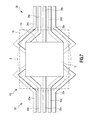
- FIG. 1 illustrates a top view of an electrical structure 4 a , in accordance with embodiments of the present invention.
- Electrical structure 4 a comprises an electrically conductive pad 12 , a plurality of wire traces 14 , a plurality of wire traces 16 , an intermediate pad 10 , a ball limiting metallurgy structure 15 (i.e., shown in FIG. 2 ), an interconnect structure 8 , an insulator layer 19 (i.e., shown in FIG. 2 ), and a photosensitive polyimide (PSPI) layer 21 (i.e., shown in FIG. 2 ).
- Interconnect structure 8 may comprise a solder material.
- Solder material is defined herein as a metal alloy comprising a low melting point (i.e., about 100 degrees Celsius to about 340 degrees Celsius) that is used to join metallic surfaces together without melting the metallic surfaces.
- a solder material may include, inter alia, an alloy of tin such as SnCu, SnAgCu, SnPb, etc.
- Interconnect structure 8 may comprise a controlled collapse chip connector (C4) solderball.
- interconnect structure 8 may comprise a non-solder metallic material (i.e., does not comprise any solder material) such as, inter alia, copper, gold, nickel, etc.
- Intermediate pad 10 may comprise, inter alia, aluminum, etc.
- Electrical structure 4 a is formed on a substrate (i.e., substrate 7 illustrated in FIG. 2 ).
- Wire traces 14 comprise a wire trace 14 a , a wire trace 14 b , a wire trace 14 c , a wire trace 14 d , and a wire trace 14 e .
- Wire trace is 14 a is electrically (and mechanically) connected to a side 12 b of electrically conductive pad 12 .
- Wire trace is 14 b is electrically connected to a side 12 a of electrically conductive pad 12 .
- the connection between wire trace 14 b and side 12 a is located adjacent to corner 18 a of electrically conductive pad 12 .
- Wire trace is 14 d is electrically connected to side 12 a of electrically conductive pad 12 .
- the connection between wire trace 14 d and side 12 a is located adjacent to corner 18 b of electrically conductive pad 12 .
- Wire trace is 14 c is electrically connected to side 12 a of electrically conductive pad 12 .
- the connection between wire trace 14 c and side 12 a is located on a portion of side 12 a located between the connection of wire trace 14 d and side 12 a and the connection of wire trace 14 b and side 12 a .
- Wire trace is 14 e is electrically connected to a side 12 c of electrically conductive pad 12 .
- Wires traces 14 a , 14 b , 14 d , and 14 e each comprise a geometry that forms a plurality of angles (i.e., 90 degree angles).
- Wire traces 14 are formed in the aforementioned configuration so that a current signal (i.e., current signal originating from other components and/or circuits on substrate 7 or substrate 33 ) traveling along wire traces 14 in a direction 5 a is evenly distributed among wire traces 14 a . . . 14 e (or alternatively traveling from electrically conductive pad 12 to wire traces 14 in a direction 5 b ).
- Electro migration is defined herein as a migration or transport of material (e.g., material comprised by interconnect structure 8 ) caused by a gradual movement of ions (e.g., in the material comprised by interconnect structure 8 ) due to a momentum exchange between conducting electrons and diffusing metal atoms. Electro migration of material comprised by interconnect structure 8 causes portions of interconnect structure 8 to comprise a reduced density of material in the portions of interconnect structure 8 .
- Wire traces 16 comprise a wire trace 16 a , a wire trace 16 b , a wire trace 16 c , a wire trace 16 d , and a wire trace 16 e .
- Wire trace is 16 a is electrically (and mechanically) connected to side 12 b of electrically conductive pad 12 .
- Wire trace is 16 b is electrically connected to side 12 d of electrically conductive pad 12 .
- the connection between wire trace 16 b and side 12 d is located adjacent to corner 18 d of electrically conductive pad 12 .
- Wire trace is 16 d is electrically connected to side 12 d of electrically conductive pad 12 .
- the connection between wire trace 16 d and side 12 d is located adjacent to corner 18 c of electrically conductive pad 12 .
- Wire trace is 14 c is electrically connected to side 12 d of electrically conductive pad 12 .
- the connection between wire trace 16 c and side 12 d is located on a portion of side 12 d located between the connection of wire trace 16 d and side 12 d and the connection of wire trace 16 b and side 12 d .
- Wire trace is 16 e is electrically connected to side 12 c of electrically conductive pad 12 .
- Wires traces 16 a , 16 b , 16 d , and 16 e each comprise a geometry that forms a plurality of angles (i.e., 90 degree angles).
- Wire traces 16 are formed in the aforementioned configuration so that a current signal (i.e., current signal originating from other components and/or circuits on substrate 7 or substrate 33 ) traveling along wire traces 16 in a direction 5 b is distributed among wire traces 16 a . . . 16 e (or alternatively traveling from electrically conductive pad 12 to wire traces 16 in a direction 5 a ).
- the current signal distributed among wire traces 16 a . . . 16 e enters electrically conductive pad 12 in discrete locations in order to reduce a current density of the current signal entering electrically conductive pad 12 and interconnect structure 8 .
- a reduction in the current density entering interconnect structure 8 reduces an electro migration of material comprised by interconnect structure 8 (e.g., solder material, non-solder material, etc).
- FIG. 2 illustrates a cross sectional view of electrical structure 4 a of FIG. 1 , in accordance with embodiments of the present invention.
- the cross sectional view of FIG. 2 is taken along line 2 - 2 of FIG. 1 .
- the cross sectional view in FIG. 2 illustrates substrate 7 , wire trace 14 c , electrically conductive pad 12 , wire trace 16 c , intermediate pad 10 , ball limiting metallurgy structure 15 , interconnect structure 8 , insulator layer 19 , photosensitive polyimide (PSPI) layer 21 , electrically conductive pad 23 , and substrate 33 .
- Electrically conductive pad 12 10 may be connected to wires or electrical components within substrate 7 .
- Electrically conductive pad 23 may be connected to wires or electrical components within substrate 33 .
- Substrate 7 may comprise, inter alia, a semiconductor device (e.g., an integrated circuit chip, a semiconductor wafer, etc), a chip carrier (organic or inorganic), a printed circuit board, etc.
- Substrate 33 may comprise, inter alia, a semiconductor device (e.g., an integrated circuit chip, a semiconductor wafer, etc), a chip carrier (organic or inorganic), a printed circuit board, etc.
- Insulator layer 19 may comprise any insulator material including, inter alia, silicon dioxide, silicon nitride, etc.
- FIG. 3 depicts a first alternative to FIG. 1 illustrating a top view of an electrical structure 4 b , in accordance with embodiments of the present invention.
- Electrical structure 4 b of FIG. 3 comprises electrical structure 4 a of FIG. 1 and electrical structure 4 c similar to electrical structure 4 a .
- Electrical structure 4 c comprises an electrically conductive pad 15 , a plurality of wire traces 24 , a plurality of wire traces 28 , an intermediate pad 10 a , a ball limiting metallurgy structure 15 (i.e., shown in FIG. 2 ), an interconnect structure 8 a , an insulator layer 19 (i.e., shown in FIG.
- Interconnect structure 8 a may comprise a solder material.
- interconnect structure 8 a may comprise a non-solder metallic material (i.e., does not comprise any solder material) such as, inter alia, copper, gold, nickel, etc.
- Intermediate pad 10 may comprise, inter alia, aluminum, etc.
- Electrical structure 4 c is formed on a substrate (i.e., substrate 7 illustrated in FIG. 2 ). Electrical structure 4 c electrically and mechanically connects components and/or circuits on substrate 7 to components and/or circuits on a second substrate (i.e., substrate 33 illustrated in FIG. 2 ).
- Wire traces 24 comprise a wire trace 24 a , a wire trace 24 b , a wire trace 24 c , a wire trace 24 d , and a wire trace 24 e .
- Wire trace is 24 a is electrically (and mechanically) connected to a side 15 b of electrically conductive pad 15 .
- Wire trace is 24 b is electrically connected to a side 15 a of electrically conductive pad 15 .
- the connection between wire trace 24 b and side 15 a is located adjacent to corner 19 a of electrically conductive pad 15 .
- Wire trace is 24 d is electrically connected to side 15 a of electrically conductive pad 15 .
- connection between wire trace 24 d and side 15 a is located adjacent to corner 198 b of electrically conductive pad 15 .
- Wire trace is 24 c is electrically connected to side 15 a of electrically conductive pad 15 .
- the connection between wire trace 24 c and side 15 a is located on a portion of side 15 a located between the connection of wire trace 24 d and side 15 a and the connection of wire trace 24 b and side 15 a .
- Wire trace is 24 e is electrically connected to a side 15 c of electrically conductive pad 15 .
- Wires traces 15 a , 15 b , 15 d , and 15 e each comprise a geometry that forms a plurality of angles (i.e., 90 degree angles).
- Wire traces 24 are formed in the aforementioned configuration so that a current signal (i.e., current signal originating from other components and/or circuits on substrate 7 or substrate 33 or from electrical structure 4 a ) traveling along wire traces 24 in a direction 5 a is evenly distributed among wire traces 24 a . . . 24 e (or alternatively traveling from electrically conductive pad 15 to wire traces 24 in a direction 5 b ).
- the current signal distributed among wire traces 24 a . . . 24 e enters electrically conductive pad 15 in discrete locations in order to reduce a current density of the current signal entering electrically conductive pad 15 and interconnect structure 8 a .
- a reduction in the current density entering interconnect structure 8 a reduces an electro migration of material comprised by interconnect structure 8 a (e.g., solder material, non-solder material, etc). Electro migration of material comprised by interconnect structure 8 a causes portions of interconnect structure 8 a to comprise a reduced density of material in the portions of interconnect structure 8 a.
- material comprised by interconnect structure 8 a e.g., solder material, non-solder material, etc.
- Wire traces 28 comprise a wire trace 28 a , a wire trace 28 b , a wire trace 28 c , a wire trace 28 d , and a wire trace 28 e .
- Wire trace is 28 a is electrically (and mechanically) connected to side 28 b of electrically conductive pad 15 .
- Wire trace is 28 b is electrically connected to side 15 d of electrically conductive pad 15 .
- the connection between wire trace 28 b and side 15 d is located adjacent to corner 19 d of electrically conductive pad 12 .
- Wire trace is 16 d is electrically connected to side 12 d of electrically conductive pad 15 .
- the connection between wire trace 28 d and side 15 d is located adjacent to corner 19 c of electrically conductive pad 15 .
- Wire trace is 14 c is electrically connected to side 12 d of electrically conductive pad 12 .
- the connection between wire trace 28 c and side 15 d is located on a portion of side 15 d located between the connection of wire trace 28 d and side 15 d and the connection of wire trace 28 b and side 15 d .
- Wire trace is 28 e is electrically connected to side 15 c of electrically conductive pad 15 .
- Wires traces 28 a , 28 b , 28 d , and 28 e each comprise a geometry that forms a plurality of angles (i.e., 90 degree angles).
- Wire traces 28 are formed in the aforementioned configuration so that a current signal (i.e., current signal originating from other components and/or circuits on substrate 7 or substrate 33 ) traveling along wire traces 16 in a direction 5 b is distributed among wire traces 28 a . . . 28 e (or alternatively traveling from electrically conductive pad 15 to wire traces 28 in a direction 5 a ).
- the current signal distributed among wire traces 28 a . . . 28 e enters electrically conductive pad 15 in discrete locations in order to reduce a current density of the current signal entering electrically conductive pad 15 and interconnect structure 8 a .
- a reduction in the current density entering interconnect structure 8 a reduces an electro migration of material comprised by interconnect structure 8 a (e.g., solder material, non-solder material, etc).
- Wire traces 16 of electrical structure 4 a are electrically and mechanically connected to wire traces 24 of electrical structure 4 c thereby electrically and mechanically connecting electrical structure 4 a to electrical structure 4 c in order to form electrical structure 4 b.
- FIG. 4 depicts a second alternative to FIG. 1 illustrating a top view of an electrical structure 4 d , in accordance with embodiments of the present invention.
- Electrical structure 4 d of FIG. 4 comprises electrical structure 4 a of FIG. 1 electrically and mechanically connected to a single wire trace 17 .
- Electrical structure 4 d is formed on a substrate (i.e., substrate 7 illustrated in FIG. 2 ).
- Electrical structure 4 d electrically and mechanically connects components and/or circuits on substrate 7 to components and/or circuits on a second substrate (i.e., substrate 33 illustrated in FIG. 2 ).
- Single wire trace 17 may be connected to electrical circuits or electrical components on substrate 7 .
- FIG. 5 depicts a first alternative to FIG. 3 and FIG. 4 illustrating a top view of an electrical structure 4 e , in accordance with embodiments of the present invention.
- Electrical structure 4 e of FIG. 5 comprises electrical structure 4 d of FIG. 4 electrically and mechanically connected to electrical structure 4 c of FIG. 3 via single wire trace 17 .
- Electrical structure 4 e is formed on a substrate (i.e., substrate 7 illustrated in FIG. 2 ).
- FIG. 6 depicts a third alternative to FIG. 1 illustrating a top view of an electrical structure 4 f , in accordance with embodiments of the present invention.
- electrical structure 4 f of FIG. 6 comprises plurality of wire traces 31 and plurality of wire traces 34 .
- Wire traces 31 comprises wire traces 31 a . . . 31 e .
- Wire traces 31 a , 31 b , 31 d , and 31 e each comprise a curved wire section mechanically and electrically connected to electrically conductive pad 12 .
- Wire traces 34 comprise wire traces 34 a . . . 34 e .
- Wire traces 34 a , 34 b , 34 d , and 34 e each comprise a curved wire section mechanically and electrically connected to electrically conductive pad 12 .
- FIG. 7 depicts a first alternative to FIG. 6 illustrating a top view of an electrical structure 4 g , in accordance with embodiments of the present invention.
- electrical structure 4 g of FIG. 7 comprises plurality of wire traces 35 and plurality of wire traces 38 .
- Wire traces 35 comprises wire traces 35 a . . . 35 e .
- Wire traces 35 a , 35 b , 35 d , and 35 e each comprise an angular wire section (i.e., comprising at least one internal angle within a traversing path of each of wire traces 35 a , 35 b , 35 d , and 35 e and may comprise a non-ninety degree angle) mechanically and electrically connected to electrically conductive pad 12 .
- Wire traces 38 comprise wire traces 38 a . . . 38 e .
- Wire traces 38 a , 38 b , 38 d , and 38 e each comprise an angular wire section (i.e., comprising at least one internal angle within a traversing path of each of wire traces 38 a , 38 b , 38 d , and 38 e and may comprise a non-ninety degree angle) mechanically and electrically connected to electrically conductive pad 12 .
Landscapes
- Engineering & Computer Science (AREA)
- Microelectronics & Electronic Packaging (AREA)
- Electric Connection Of Electric Components To Printed Circuits (AREA)
- Printing Elements For Providing Electric Connections Between Printed Circuits (AREA)
Abstract
Description
Claims (15)
Priority Applications (1)
| Application Number | Priority Date | Filing Date | Title |
|---|---|---|---|
| US12/957,431 US8819933B2 (en) | 2007-10-16 | 2010-12-01 | Method for forming a current distribution structure |
Applications Claiming Priority (2)
| Application Number | Priority Date | Filing Date | Title |
|---|---|---|---|
| US11/872,870 US7911803B2 (en) | 2007-10-16 | 2007-10-16 | Current distribution structure and method |
| US12/957,431 US8819933B2 (en) | 2007-10-16 | 2010-12-01 | Method for forming a current distribution structure |
Related Parent Applications (1)
| Application Number | Title | Priority Date | Filing Date |
|---|---|---|---|
| US11/872,870 Division US7911803B2 (en) | 2007-10-16 | 2007-10-16 | Current distribution structure and method |
Publications (2)
| Publication Number | Publication Date |
|---|---|
| US20110072656A1 US20110072656A1 (en) | 2011-03-31 |
| US8819933B2 true US8819933B2 (en) | 2014-09-02 |
Family
ID=40533078
Family Applications (2)
| Application Number | Title | Priority Date | Filing Date |
|---|---|---|---|
| US11/872,870 Expired - Fee Related US7911803B2 (en) | 2007-10-16 | 2007-10-16 | Current distribution structure and method |
| US12/957,431 Expired - Fee Related US8819933B2 (en) | 2007-10-16 | 2010-12-01 | Method for forming a current distribution structure |
Family Applications Before (1)
| Application Number | Title | Priority Date | Filing Date |
|---|---|---|---|
| US11/872,870 Expired - Fee Related US7911803B2 (en) | 2007-10-16 | 2007-10-16 | Current distribution structure and method |
Country Status (1)
| Country | Link |
|---|---|
| US (2) | US7911803B2 (en) |
Families Citing this family (8)
| Publication number | Priority date | Publication date | Assignee | Title |
|---|---|---|---|---|
| US8084858B2 (en) | 2009-04-15 | 2011-12-27 | International Business Machines Corporation | Metal wiring structures for uniform current density in C4 balls |
| US8889995B2 (en) * | 2011-03-03 | 2014-11-18 | Skyworks Solutions, Inc. | Wire bond pad system and method |
| US8487447B2 (en) | 2011-05-19 | 2013-07-16 | International Business Machines Corporation | Semiconductor structure having offset passivation to reduce electromigration |
| US9679869B2 (en) | 2011-09-02 | 2017-06-13 | Skyworks Solutions, Inc. | Transmission line for high performance radio frequency applications |
| US9123544B2 (en) | 2011-10-21 | 2015-09-01 | Infineon Technologies Ag | Semiconductor device and method |
| KR102250612B1 (en) | 2012-06-14 | 2021-05-10 | 스카이워크스 솔루션즈, 인코포레이티드 | Power amplifier modules with harmonic termination circuit and related systems, devices, and methods |
| DE102012214982B4 (en) * | 2012-08-23 | 2021-06-02 | Vitesco Technologies GmbH | Printed circuit board |
| US9515035B2 (en) | 2014-12-19 | 2016-12-06 | International Business Machines Corporation | Three-dimensional integrated circuit integration |
Citations (13)
| Publication number | Priority date | Publication date | Assignee | Title |
|---|---|---|---|---|
| US5101261A (en) | 1988-09-09 | 1992-03-31 | Texas Instruments Incorporated | Electronic circuit device with electronomigration-resistant metal conductors |
| US5712510A (en) | 1995-08-04 | 1998-01-27 | Advanced Micro Devices, Inc. | Reduced electromigration interconnection line |
| US6320262B1 (en) | 1997-12-05 | 2001-11-20 | Ricoh Company, Ltd. | Semiconductor device and manufacturing method thereof |
| US6566611B2 (en) | 2001-09-26 | 2003-05-20 | Intel Corporation | Anti-tombstoning structures and methods of manufacture |
| US20030173684A1 (en) | 2002-03-12 | 2003-09-18 | Rajeev Joshi | Wafer-level coated copper stud bumps |
| US6822327B1 (en) * | 2003-06-13 | 2004-11-23 | Delphi Technologies, Inc. | Flip-chip interconnected with increased current-carrying capability |
| US20050158980A1 (en) | 2000-06-28 | 2005-07-21 | Krishna Seshan | Method of forming segmented ball limiting metallurgy |
| US7042098B2 (en) * | 2003-07-07 | 2006-05-09 | Freescale Semiconductor,Inc | Bonding pad for a packaged integrated circuit |
| US20060170100A1 (en) | 2005-02-01 | 2006-08-03 | Richling Wayne P | Routing design to minimize electromigration damage to solder bumps |
| US20060186539A1 (en) | 2005-02-01 | 2006-08-24 | Dauksher Walter J | Trace design to minimize electromigration damage to solder bumps |
| US20060211167A1 (en) | 2005-03-18 | 2006-09-21 | International Business Machines Corporation | Methods and systems for improving microelectronic i/o current capabilities |
| US7297631B2 (en) | 2002-06-25 | 2007-11-20 | Unitive International Limited | Methods of forming electronic structures including conductive shunt layers and related structures |
| US20090286108A1 (en) | 2008-05-15 | 2009-11-19 | Samsung Electronics Co., Ltd. | Hybrid electronic device including semiconductor chip and fuel cell, method of fabricating the same and system having the same |
-
2007
- 2007-10-16 US US11/872,870 patent/US7911803B2/en not_active Expired - Fee Related
-
2010
- 2010-12-01 US US12/957,431 patent/US8819933B2/en not_active Expired - Fee Related
Patent Citations (15)
| Publication number | Priority date | Publication date | Assignee | Title |
|---|---|---|---|---|
| US5101261A (en) | 1988-09-09 | 1992-03-31 | Texas Instruments Incorporated | Electronic circuit device with electronomigration-resistant metal conductors |
| US5712510A (en) | 1995-08-04 | 1998-01-27 | Advanced Micro Devices, Inc. | Reduced electromigration interconnection line |
| US6320262B1 (en) | 1997-12-05 | 2001-11-20 | Ricoh Company, Ltd. | Semiconductor device and manufacturing method thereof |
| US20050158980A1 (en) | 2000-06-28 | 2005-07-21 | Krishna Seshan | Method of forming segmented ball limiting metallurgy |
| US7034402B1 (en) | 2000-06-28 | 2006-04-25 | Intel Corporation | Device with segmented ball limiting metallurgy |
| US6566611B2 (en) | 2001-09-26 | 2003-05-20 | Intel Corporation | Anti-tombstoning structures and methods of manufacture |
| US20030173684A1 (en) | 2002-03-12 | 2003-09-18 | Rajeev Joshi | Wafer-level coated copper stud bumps |
| US7297631B2 (en) | 2002-06-25 | 2007-11-20 | Unitive International Limited | Methods of forming electronic structures including conductive shunt layers and related structures |
| US6822327B1 (en) * | 2003-06-13 | 2004-11-23 | Delphi Technologies, Inc. | Flip-chip interconnected with increased current-carrying capability |
| US7042098B2 (en) * | 2003-07-07 | 2006-05-09 | Freescale Semiconductor,Inc | Bonding pad for a packaged integrated circuit |
| US20060170100A1 (en) | 2005-02-01 | 2006-08-03 | Richling Wayne P | Routing design to minimize electromigration damage to solder bumps |
| US20060186539A1 (en) | 2005-02-01 | 2006-08-24 | Dauksher Walter J | Trace design to minimize electromigration damage to solder bumps |
| US7208843B2 (en) * | 2005-02-01 | 2007-04-24 | Avago Technologies General Ip (Singapore) Pte. Ltd. | Routing design to minimize electromigration damage to solder bumps |
| US20060211167A1 (en) | 2005-03-18 | 2006-09-21 | International Business Machines Corporation | Methods and systems for improving microelectronic i/o current capabilities |
| US20090286108A1 (en) | 2008-05-15 | 2009-11-19 | Samsung Electronics Co., Ltd. | Hybrid electronic device including semiconductor chip and fuel cell, method of fabricating the same and system having the same |
Non-Patent Citations (1)
| Title |
|---|
| Notice of Allowance (Mail Date Nov. 16, 2010) for U.S. Appl. No. 11/872,870, filed Oct. 16, 2007, Confirmation No. 9667. |
Also Published As
| Publication number | Publication date |
|---|---|
| US20090095519A1 (en) | 2009-04-16 |
| US7911803B2 (en) | 2011-03-22 |
| US20110072656A1 (en) | 2011-03-31 |
Similar Documents
| Publication | Publication Date | Title |
|---|---|---|
| US8819933B2 (en) | Method for forming a current distribution structure | |
| US7312529B2 (en) | Structure and method for producing multiple size interconnections | |
| US6635960B2 (en) | Angled edge connections for multichip structures | |
| US7935408B2 (en) | Substrate anchor structure and method | |
| US10163844B2 (en) | Semiconductor device having conductive bumps of varying heights | |
| US20080026560A1 (en) | Methods of forming electronic structures including conductive shunt layers and related structures | |
| US8125789B2 (en) | Wiring substrate and electronic device | |
| US6894378B2 (en) | Electronic component with stacked semiconductor chips | |
| US8441127B2 (en) | Bump-on-trace structures with wide and narrow portions | |
| KR101140469B1 (en) | A routing design to minimize electromigration damage to solder bumps | |
| US20090273098A1 (en) | Enhanced Architectural Interconnect Options Enabled With Flipped Die on a Multi-Chip Package | |
| US6661100B1 (en) | Low impedance power distribution structure for a semiconductor chip package | |
| JP4916241B2 (en) | Semiconductor device and manufacturing method thereof | |
| US7872358B2 (en) | Semiconductor chip and semiconductor device, and method for manufacturing semiconductor device | |
| US9171812B1 (en) | Semiconductor device having conductive pads with neck-down portions to prevent solder reflow | |
| US10090274B2 (en) | Flip chip interconnection with reduced current density | |
| TWI495052B (en) | Substrate structure and semiconductor package using the same | |
| US20100109167A1 (en) | Conductive paths for transmitting an electrical signal through an electrical connector | |
| US7208830B2 (en) | Interconnect shunt used for current distribution and reliability redundancy | |
| US12057404B2 (en) | Semiconductor device | |
| US12532766B2 (en) | Electronic package and electronic structure thereof | |
| EP0844664A2 (en) | A bond pad for an integrated circuit | |
| KR20070014015A (en) | Semiconductor devices | |
| US20050104213A1 (en) | Electric connection terminal and method of manufacturing the same, semiconductor device and method of mounting the same | |
| JPH10126029A (en) | Wiring board for mounting BGA type components and mounting circuit device |
Legal Events
| Date | Code | Title | Description |
|---|---|---|---|
| AS | Assignment |
Owner name: GLOBALFOUNDRIES U.S. 2 LLC, NEW YORK Free format text: ASSIGNMENT OF ASSIGNORS INTEREST;ASSIGNOR:INTERNATIONAL BUSINESS MACHINES CORPORATION;REEL/FRAME:036550/0001 Effective date: 20150629 |
|
| AS | Assignment |
Owner name: GLOBALFOUNDRIES INC., CAYMAN ISLANDS Free format text: ASSIGNMENT OF ASSIGNORS INTEREST;ASSIGNORS:GLOBALFOUNDRIES U.S. 2 LLC;GLOBALFOUNDRIES U.S. INC.;REEL/FRAME:036779/0001 Effective date: 20150910 |
|
| FEPP | Fee payment procedure |
Free format text: MAINTENANCE FEE REMINDER MAILED (ORIGINAL EVENT CODE: REM.) |
|
| LAPS | Lapse for failure to pay maintenance fees |
Free format text: PATENT EXPIRED FOR FAILURE TO PAY MAINTENANCE FEES (ORIGINAL EVENT CODE: EXP.); ENTITY STATUS OF PATENT OWNER: LARGE ENTITY |
|
| STCH | Information on status: patent discontinuation |
Free format text: PATENT EXPIRED DUE TO NONPAYMENT OF MAINTENANCE FEES UNDER 37 CFR 1.362 |
|
| FP | Lapsed due to failure to pay maintenance fee |
Effective date: 20180902 |
|
| AS | Assignment |
Owner name: GLOBALFOUNDRIES U.S. INC., NEW YORK Free format text: RELEASE BY SECURED PARTY;ASSIGNOR:WILMINGTON TRUST, NATIONAL ASSOCIATION;REEL/FRAME:056987/0001 Effective date: 20201117 Owner name: GLOBALFOUNDRIES U.S. INC., NEW YORK Free format text: RELEASE OF SECURITY INTEREST;ASSIGNOR:WILMINGTON TRUST, NATIONAL ASSOCIATION;REEL/FRAME:056987/0001 Effective date: 20201117 |