US8815730B1 - Method for forming bond pad stack for transistors - Google Patents
Method for forming bond pad stack for transistors Download PDFInfo
- Publication number
- US8815730B1 US8815730B1 US13/934,956 US201313934956A US8815730B1 US 8815730 B1 US8815730 B1 US 8815730B1 US 201313934956 A US201313934956 A US 201313934956A US 8815730 B1 US8815730 B1 US 8815730B1
- Authority
- US
- United States
- Prior art keywords
- metal layer
- bond pad
- layer
- metal
- dielectric layer
- Prior art date
- Legal status (The legal status is an assumption and is not a legal conclusion. Google has not performed a legal analysis and makes no representation as to the accuracy of the status listed.)
- Active
Links
Images


Classifications
-
- H—ELECTRICITY
- H10—SEMICONDUCTOR DEVICES; ELECTRIC SOLID-STATE DEVICES NOT OTHERWISE PROVIDED FOR
- H10D—INORGANIC ELECTRIC SEMICONDUCTOR DEVICES
- H10D30/00—Field-effect transistors [FET]
- H10D30/60—Insulated-gate field-effect transistors [IGFET]
- H10D30/64—Double-diffused metal-oxide semiconductor [DMOS] FETs
- H10D30/66—Vertical DMOS [VDMOS] FETs
-
- H—ELECTRICITY
- H10—SEMICONDUCTOR DEVICES; ELECTRIC SOLID-STATE DEVICES NOT OTHERWISE PROVIDED FOR
- H10W—GENERIC PACKAGES, INTERCONNECTIONS, CONNECTORS OR OTHER CONSTRUCTIONAL DETAILS OF DEVICES COVERED BY CLASS H10
- H10W20/00—Interconnections in chips, wafers or substrates
- H10W20/40—Interconnections external to wafers or substrates, e.g. back-end-of-line [BEOL] metallisations or vias connecting to gate electrodes
-
- H01L24/05—
-
- H01L24/03—
-
- H—ELECTRICITY
- H10—SEMICONDUCTOR DEVICES; ELECTRIC SOLID-STATE DEVICES NOT OTHERWISE PROVIDED FOR
- H10W—GENERIC PACKAGES, INTERCONNECTIONS, CONNECTORS OR OTHER CONSTRUCTIONAL DETAILS OF DEVICES COVERED BY CLASS H10
- H10W70/00—Package substrates; Interposers; Redistribution layers [RDL]
- H10W70/40—Leadframes
- H10W70/464—Additional interconnections in combination with leadframes
- H10W70/466—Tape carriers or flat leads
-
- H—ELECTRICITY
- H10—SEMICONDUCTOR DEVICES; ELECTRIC SOLID-STATE DEVICES NOT OTHERWISE PROVIDED FOR
- H10W—GENERIC PACKAGES, INTERCONNECTIONS, CONNECTORS OR OTHER CONSTRUCTIONAL DETAILS OF DEVICES COVERED BY CLASS H10
- H10W70/00—Package substrates; Interposers; Redistribution layers [RDL]
- H10W70/40—Leadframes
- H10W70/481—Leadframes for devices being provided for in groups H10D8/00 - H10D48/00
-
- H—ELECTRICITY
- H10—SEMICONDUCTOR DEVICES; ELECTRIC SOLID-STATE DEVICES NOT OTHERWISE PROVIDED FOR
- H10W—GENERIC PACKAGES, INTERCONNECTIONS, CONNECTORS OR OTHER CONSTRUCTIONAL DETAILS OF DEVICES COVERED BY CLASS H10
- H10W72/00—Interconnections or connectors in packages
- H10W72/01—Manufacture or treatment
- H10W72/019—Manufacture or treatment of bond pads
- H10W72/01931—Manufacture or treatment of bond pads using blanket deposition
- H10W72/01933—Manufacture or treatment of bond pads using blanket deposition in liquid form, e.g. spin coating, spray coating or immersion coating
- H10W72/01935—Manufacture or treatment of bond pads using blanket deposition in liquid form, e.g. spin coating, spray coating or immersion coating by plating, e.g. electroless plating or electroplating
-
- H—ELECTRICITY
- H10—SEMICONDUCTOR DEVICES; ELECTRIC SOLID-STATE DEVICES NOT OTHERWISE PROVIDED FOR
- H10W—GENERIC PACKAGES, INTERCONNECTIONS, CONNECTORS OR OTHER CONSTRUCTIONAL DETAILS OF DEVICES COVERED BY CLASS H10
- H10W72/00—Interconnections or connectors in packages
- H10W72/01—Manufacture or treatment
- H10W72/019—Manufacture or treatment of bond pads
- H10W72/01931—Manufacture or treatment of bond pads using blanket deposition
- H10W72/01938—Manufacture or treatment of bond pads using blanket deposition in gaseous form, e.g. by CVD or PVD
-
- H—ELECTRICITY
- H10—SEMICONDUCTOR DEVICES; ELECTRIC SOLID-STATE DEVICES NOT OTHERWISE PROVIDED FOR
- H10W—GENERIC PACKAGES, INTERCONNECTIONS, CONNECTORS OR OTHER CONSTRUCTIONAL DETAILS OF DEVICES COVERED BY CLASS H10
- H10W72/00—Interconnections or connectors in packages
- H10W72/01—Manufacture or treatment
- H10W72/019—Manufacture or treatment of bond pads
- H10W72/01951—Changing the shapes of bond pads
- H10W72/01953—Changing the shapes of bond pads by etching
-
- H—ELECTRICITY
- H10—SEMICONDUCTOR DEVICES; ELECTRIC SOLID-STATE DEVICES NOT OTHERWISE PROVIDED FOR
- H10W—GENERIC PACKAGES, INTERCONNECTIONS, CONNECTORS OR OTHER CONSTRUCTIONAL DETAILS OF DEVICES COVERED BY CLASS H10
- H10W72/00—Interconnections or connectors in packages
- H10W72/01—Manufacture or treatment
- H10W72/0198—Manufacture or treatment batch processes
-
- H—ELECTRICITY
- H10—SEMICONDUCTOR DEVICES; ELECTRIC SOLID-STATE DEVICES NOT OTHERWISE PROVIDED FOR
- H10W—GENERIC PACKAGES, INTERCONNECTIONS, CONNECTORS OR OTHER CONSTRUCTIONAL DETAILS OF DEVICES COVERED BY CLASS H10
- H10W72/00—Interconnections or connectors in packages
- H10W72/50—Bond wires
- H10W72/59—Bond pads specially adapted therefor
-
- H—ELECTRICITY
- H10—SEMICONDUCTOR DEVICES; ELECTRIC SOLID-STATE DEVICES NOT OTHERWISE PROVIDED FOR
- H10W—GENERIC PACKAGES, INTERCONNECTIONS, CONNECTORS OR OTHER CONSTRUCTIONAL DETAILS OF DEVICES COVERED BY CLASS H10
- H10W72/00—Interconnections or connectors in packages
- H10W72/851—Dispositions of multiple connectors or interconnections
- H10W72/874—On different surfaces
- H10W72/884—Die-attach connectors and bond wires
-
- H—ELECTRICITY
- H10—SEMICONDUCTOR DEVICES; ELECTRIC SOLID-STATE DEVICES NOT OTHERWISE PROVIDED FOR
- H10W—GENERIC PACKAGES, INTERCONNECTIONS, CONNECTORS OR OTHER CONSTRUCTIONAL DETAILS OF DEVICES COVERED BY CLASS H10
- H10W72/00—Interconnections or connectors in packages
- H10W72/90—Bond pads, in general
- H10W72/921—Structures or relative sizes of bond pads
- H10W72/923—Bond pads having multiple stacked layers
-
- H—ELECTRICITY
- H10—SEMICONDUCTOR DEVICES; ELECTRIC SOLID-STATE DEVICES NOT OTHERWISE PROVIDED FOR
- H10W—GENERIC PACKAGES, INTERCONNECTIONS, CONNECTORS OR OTHER CONSTRUCTIONAL DETAILS OF DEVICES COVERED BY CLASS H10
- H10W72/00—Interconnections or connectors in packages
- H10W72/90—Bond pads, in general
- H10W72/941—Dispositions of bond pads
- H10W72/9415—Dispositions of bond pads relative to the surface, e.g. recessed, protruding
-
- H—ELECTRICITY
- H10—SEMICONDUCTOR DEVICES; ELECTRIC SOLID-STATE DEVICES NOT OTHERWISE PROVIDED FOR
- H10W—GENERIC PACKAGES, INTERCONNECTIONS, CONNECTORS OR OTHER CONSTRUCTIONAL DETAILS OF DEVICES COVERED BY CLASS H10
- H10W72/00—Interconnections or connectors in packages
- H10W72/90—Bond pads, in general
- H10W72/941—Dispositions of bond pads
- H10W72/942—Dispositions of bond pads relative to underlying supporting features, e.g. bond pads, RDLs or vias
-
- H—ELECTRICITY
- H10—SEMICONDUCTOR DEVICES; ELECTRIC SOLID-STATE DEVICES NOT OTHERWISE PROVIDED FOR
- H10W—GENERIC PACKAGES, INTERCONNECTIONS, CONNECTORS OR OTHER CONSTRUCTIONAL DETAILS OF DEVICES COVERED BY CLASS H10
- H10W72/00—Interconnections or connectors in packages
- H10W72/90—Bond pads, in general
- H10W72/951—Materials of bond pads
- H10W72/952—Materials of bond pads comprising metals or metalloids, e.g. PbSn, Ag or Cu
-
- H—ELECTRICITY
- H10—SEMICONDUCTOR DEVICES; ELECTRIC SOLID-STATE DEVICES NOT OTHERWISE PROVIDED FOR
- H10W—GENERIC PACKAGES, INTERCONNECTIONS, CONNECTORS OR OTHER CONSTRUCTIONAL DETAILS OF DEVICES COVERED BY CLASS H10
- H10W74/00—Encapsulations, e.g. protective coatings
- H10W74/10—Encapsulations, e.g. protective coatings characterised by their shape or disposition
- H10W74/131—Encapsulations, e.g. protective coatings characterised by their shape or disposition the semiconductor body being only partially enclosed
- H10W74/147—Encapsulations, e.g. protective coatings characterised by their shape or disposition the semiconductor body being only partially enclosed the encapsulations being multilayered
-
- H—ELECTRICITY
- H10—SEMICONDUCTOR DEVICES; ELECTRIC SOLID-STATE DEVICES NOT OTHERWISE PROVIDED FOR
- H10W—GENERIC PACKAGES, INTERCONNECTIONS, CONNECTORS OR OTHER CONSTRUCTIONAL DETAILS OF DEVICES COVERED BY CLASS H10
- H10W90/00—Package configurations
- H10W90/701—Package configurations characterised by the relative positions of pads or connectors relative to package parts
- H10W90/731—Package configurations characterised by the relative positions of pads or connectors relative to package parts of die-attach connectors
- H10W90/736—Package configurations characterised by the relative positions of pads or connectors relative to package parts of die-attach connectors between a chip and a stacked lead frame, conducting package substrate or heat sink
-
- H—ELECTRICITY
- H10—SEMICONDUCTOR DEVICES; ELECTRIC SOLID-STATE DEVICES NOT OTHERWISE PROVIDED FOR
- H10W—GENERIC PACKAGES, INTERCONNECTIONS, CONNECTORS OR OTHER CONSTRUCTIONAL DETAILS OF DEVICES COVERED BY CLASS H10
- H10W90/00—Package configurations
- H10W90/701—Package configurations characterised by the relative positions of pads or connectors relative to package parts
- H10W90/751—Package configurations characterised by the relative positions of pads or connectors relative to package parts of bond wires
- H10W90/756—Package configurations characterised by the relative positions of pads or connectors relative to package parts of bond wires between a chip and a stacked lead frame, conducting package substrate or heat sink
-
- H—ELECTRICITY
- H10—SEMICONDUCTOR DEVICES; ELECTRIC SOLID-STATE DEVICES NOT OTHERWISE PROVIDED FOR
- H10W—GENERIC PACKAGES, INTERCONNECTIONS, CONNECTORS OR OTHER CONSTRUCTIONAL DETAILS OF DEVICES COVERED BY CLASS H10
- H10W90/00—Package configurations
- H10W90/701—Package configurations characterised by the relative positions of pads or connectors relative to package parts
- H10W90/761—Package configurations characterised by the relative positions of pads or connectors relative to package parts of strap connectors
- H10W90/766—Package configurations characterised by the relative positions of pads or connectors relative to package parts of strap connectors between a chip and a stacked lead frame, conducting package substrate or heat sink
Definitions
- Disclosed embodiments relate generally to topside bond pad structures that connect to terminals of transistors, and methods for forming the same.
- Aluminum is a common material for semiconductor device (semiconductor die) bond pad metallization since its introduction to the semiconductor world, including for discrete transistors and integrated circuits (IC).
- IC integrated circuits
- aluminum and high aluminum alloys quickly form a refractory ceramic oxide on the surface that requires special treatment to remove before achieving successful soldering thereto. This step is applied to most of the methods in making interconnections from the aluminum bond pad on the semiconductor die built on a semiconductor substrate, usually on single-crystal silicon.
- the semiconductor die is packaged in a hermetically sealed case or a non-hermetic plastic capsule, with leads extending from bond pads on the chip to the leadframe.
- EIG electroless nickel immersion gold
- UBM Under Bump Metallization
- the surface treatments starts with surface cleaning to remove any contaminant present on the aluminum bond pad surface, followed by an activation process to activate the bond pads for better nucleation for subsequent processing through the micro-etching of aluminum oxide.
- a pre-plating process known as zincation is commonly used. During the zincation process, aluminum oxide is removed and is replaced with a thin layer of zinc metal. The zinc protects the aluminum from re-oxidation until it is ready to be plated. Once this process is performed, the aluminum coated zinc can then be electrolessly plated with nickel followed by immersion gold.
- Disclosed embodiments describe methods for forming bond pad stacks on a semiconductor die including at least one transistor having a terminal connected to a bond pad comprising a bond pad metal with a dielectric stack thereon having a contact hole on the bond pad.
- the dielectric stack includes a top dielectric layer on a bottom dielectric layer, wherein an outer edge of the bottom dielectric layer is within the contact hole and extends beyond an outer edge of the top dielectric layer to define an exposed bond pad area having a bond pad edge.
- a second metal layer on a first metal layer is deposited on the bond pad metal.
- Wet metal etch processing using a first metal mask and a second metal mask having mask edges recessed from the top dielectric layer results in recessing the second metal layer from sidewalls of the first metal layer, recessing the first metal layer from the top dielectric layer, and the first metal layer extending over the bond pad edge onto the bottom dielectric layer.
- FIG. 1 is a flow chart that shows steps in an example method for forming for forming bond pad stacks on a semiconductor die, according to an example embodiment.
- FIGS. 2A-F are cross-sectional diagrams showing processing progression for an example method of forming bond pad stacks on a semiconductor die, according to an example embodiment.
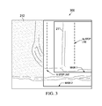
- FIG. 3 is a depiction based a scanning electron microscope (SEM) of an example completed bond pad stack having metal mask edges for metal mask 1 and metal mask 2 added to show disclosed metal mask features and resulting post-etch metal layer edges.
- SEM scanning electron microscope
- Example embodiments are described with reference to the drawings, wherein like reference numerals are used to designate similar or equivalent elements. Illustrated ordering of acts or events should not be considered as limiting, as some acts or events may occur in different order and/or concurrently with other acts or events. Furthermore, some illustrated acts or events may not be required to implement a methodology in accordance with this disclosure.
- FIG. 1 is a flow chart that shows steps in an example method 100 for forming bond pad stacks on a semiconductor die that is described together with FIGS. 2A-F which are cross-sectional diagrams showing processing progression for method 100 shown forming bond pad stacks on a semiconductor die comprising a power vertical metal oxide semiconductor (MOS) transistor, according to an example embodiment.
- Step 101 comprises providing a substrate including at least one transistor having a topside semiconductor surface, wherein a first terminal of the transistor is connected to a bond pad comprising a bond pad metal on the topside semiconductor surface.
- the bond pad material can comprise aluminum (Al) in one embodiment. However, the bond pad material can comprise other metals, such as copper, and can also comprise metal alloys.
- the transistor can be a power MOS transistor having gate electrode on a gate dielectric on a topside semiconductor surface of the substrate.
- the power transistor can include bipolars including thyristors (pair of tightly coupled bipolar junction transistors also called silicon controlled rectifiers), field effect transistors (FETs) including junction gate field-effect transistors (JFETs), and metal-oxide-semiconductor field-effect transistors (MOSFETs) including double-diffused metal-oxide-semiconductor (DMOS), High-electron-mobility transistors (HEMTs, such as a GaN HEMT), as well as Insulated Gate Bipolar Transistors (IGBTs).
- Example substrates include silicon and GaN, and the topside semiconductor surface can be the same as the substrate material, or be different.
- Step 102 comprises forming a dielectric stack including a bottom dielectric layer and a top dielectric layer on the bottom dielectric layer having a contact hole through the dielectric stack over the bond pad.
- the bottom dielectric layer is a dielectric stack including silicon nitride layer on a tetraethyl orthosilicate (TEOS) derived silicon oxide layer on a silicon oxynitride layer
- the second dielectric layer is a polyimide layer thicker than the bottom dielectric layer.
- An outer edge of the bottom dielectric layer within the contact hole extends beyond an outer edge of the top dielectric layer to define an exposed bond pad area having a bond pad edge.
- FIG. 2A is a cross sectional depiction of a semiconductor die 200 having a partially completed bond pad structure showing the substrate 205 with a topside semiconductor surface 206 having a dielectric stack thereon including a bottom dielectric layer 211 and a top dielectric layer 212 having a contact hole 239 through the dielectric stack over the bond pad 215 .
- the transistor is shown as an example n-channel vertical double diffused MOS (VDMOS) power transistor 220 that has a first terminal shown as its gate electrode 221 on a gate dielectric 229 connected to the bond pad 215 .
- the drain of transistor 220 is shown as 222 and the source as 223 , with a source contact 223 a on the bottom side of the substrate 205 .
- Transistor 220 includes p-body 224 .
- the drain 222 is generally connected to a disclosed bond pad.
- An outer edge of the bottom dielectric layer 211 within the contact hole 239 can be seen to extend beyond an outer edge of the top dielectric layer 212 to result in the bond pad 215 having an exposed bond pad area having a bond pad edge.
- Step 103 a comprises depositing a first metal layer
- step 103 b comprises depositing a second metal layer on the first metal layer.
- the depositing of the first metal layer and depositing the second metal layer can both comprise sputtering. However, plating may also be used to deposit either of these metal layers.
- FIG. 2B is a cross sectional depiction of the semiconductor die 230 having the partially completed bond pad structure showing a second metal layer 227 on a first metal layer 226 including over the bond pad 215 .
- the first metal layer 226 can comprise nickel (Ni).
- the wet etchant for etching the first metal layer 226 can comprise nitric acid (HNO 3 ).
- the second metal layer 227 can comprise metals including silver and gold.
- Step 104 comprises forming a first photoresist layer exclusively within the contact hole 239 .
- the mask used for this step is referred to herein as metal mask 1 .
- the metal mask 1 edge is on the bottom dielectric layer 211 but within the top dielectric layer 212 , and thus exclusively within the contact hole 239 .
- FIG. 3 shows a depiction based a scanning electron microscope (SEM) of an example completed bond pad stack having metal mask edges added to show disclosed metal mask features and resulting metal layer edges.
- Photolithography using metal mask 1 forms a photoresist pattern with the first photoresist layer exclusively within the contact hole 239 .
- FIG. 2C is a cross sectional depiction of semiconductor die 240 having the partially completed bond pad structure showing the first photoresist layer 233 being exclusively within the contact hole 239 over the bond pad 215 .
- Step 105 comprises wet etching the second metal layer 227 to recess the second metal layer 227 from sidewalls of the bottom dielectric layer 211 in the contact hole 239 .
- the wet etchant for etching the second metal layer 227 in the case the second metal layer comprises Ag can comprise using a mixture of sulfuric acid (H 2 SO 4 ) and phosphoric acid (H 3 PO 4 )
- FIG. 2D is a cross sectional depiction of the semiconductor die 250 showing the partially completed bond pad structure after wet etching of the second metal layer 227 to recess the second metal layer 227 from sidewalls of the bottom dielectric layer 211 in the contact hole 239 .
- Step 106 comprises forming a second photoresist layer exclusively within the contact hole.
- the mask used for this step is referred to herein as metal mask 2 .
- the metal mask 2 edge is on the bottom dielectric layer 211 but within the top dielectric layer 212 , and is thus exclusively within the contact hole 239 . See also FIG. 3 described below which shows a depiction based on a SEM of an example completed bond pad stack having metal mask edges added to show disclosed metal mask features and resulting metal layer edges.
- FIG. 2E is a cross sectional depiction of the semiconductor die 260 having the partially completed bond pad structure showing the second photoresist layer 234 exclusively within the contact hole 239 .
- Step 107 comprises wet etching the first metal layer 226 to recess the first metal layer 226 from the top dielectric layer 212 , wherein the first metal layer 226 extends over the bond pad edge onto the bottom dielectric layer 211 .
- FIG. 2F is a cross sectional depiction of the semiconductor die 270 having the completed bond pad structure showing the first metal layer 226 recessed from the top dielectric layer 212 and extending over the bond pad edge of the bond pad 215 onto the bottom dielectric layer 211 , and the second metal layer 227 on and within the area of the first metal layer 226 .
- the packaging includes solder mediated stacking of two (2) NMOS power vertical power transistors (such as each being VDMOS power transistor 220 in FIG. 2A ) with a first vertical power transistor source side down on a leadframe that is on a printed circuit board (PCB), a first metal clip on the drain side of the first vertical power transistor connected to a lead of the leadframe, a second vertical power transistor drain side down on the first metal clip, and a second metal clip on the source side of the second vertical power transistor connected to a lead of the leadframe.
- Bond wire connection can be made from disclosed bond pads connected to the respective gate electrodes of the first vertical power transistor and second vertical power transistor to leads of the leadframe.
- FIG. 3 is a depiction 300 based a SEM of an example completed bond pad stack having metal mask edges added to show disclosed metal mask features and resulting metal layer edges.
- the second metal layer is referred as Ag
- the first metal layer as Ni.
- the bottom dielectric layer 211 and top dielectric layer 212 are shown.
- the second metal edge shown as a broken line with the title “Ag stop line” is shown recessed from the edge of the bottom dielectric layer 211 a distance that is determined by the metal mask 1 pattern edge shown on the bottom dielectric layer 211 together with lateral etching of the Ag layer from the wet etch process.
- the mask pattern has been found to determine the Ni layer resulting profile, so that the resulting profile where the resulting Ni layer edge stops can be controlled by increasing or reducing the wet etching time.
- the gap shown between the edge of metal mask 1 and the top dielectric layer 212 has been found to have a significant influence to the resulting Ni profile. The more space there is, the higher the lateral etching rate. Accordingly, based on the pattern size, it has been found to be possible to set difference spaces to get a higher or lower etch rate, enabling better process control especially on smaller patterns.
- step plating which can occur in conventional metal plating processes over Al bond pads where the Ni does not extend over all bond pad metal edges. Missing Ni along any of the bond pad edge generally results in wafer scrap due to exposed Al on the bond pad.
- a challenge in conventional metal plating processes is the difficulty in controlling the Ni on the Al bond pads with good uniformity, as different Ni profiles at different sidewall locations even on one bond pad has been found to result.
- Metal sputter has been found to provide better uniformity control and essentially the same Ni profile for each die after wet etching.
- the minimum bond pad size actually fabricated was about 1 mm by 0.7 mm.
- disclosed methods are suitable for bond pad sizes down to at least to about 0.5 mm by 0.5 mm.
- Disclosed embodiments can be used to form semiconductor die including discrete devices such as power transistors or ICs that may integrated into a variety of assembly flows to form a variety of different devices and related products.
- the semiconductor die may include various elements therein and/or layers thereon, including barrier layers, dielectric layers, device structures, active elements and passive elements including source regions, drain regions, bit lines, bases, emitters, collectors, conductive lines, conductive vias, etc.
- the semiconductor die can be formed from a variety of processes including bipolar, CMOS, BiCMOS and MEMS.
Landscapes
- Internal Circuitry In Semiconductor Integrated Circuit Devices (AREA)
- Electrodes Of Semiconductors (AREA)
- Wire Bonding (AREA)
- Engineering & Computer Science (AREA)
- Manufacturing & Machinery (AREA)
Abstract
Description
Claims (6)
Priority Applications (4)
| Application Number | Priority Date | Filing Date | Title |
|---|---|---|---|
| US13/934,956 US8815730B1 (en) | 2013-07-03 | 2013-07-03 | Method for forming bond pad stack for transistors |
| PCT/US2014/045468 WO2015003163A1 (en) | 2013-07-03 | 2014-07-03 | Bond pad stack for transistors |
| CN201480037406.5A CN105359261B (en) | 2013-07-03 | 2014-07-03 | It is stacked for the bonding welding pad of transistor |
| US14/334,738 US9030023B2 (en) | 2013-07-03 | 2014-07-18 | Bond pad stack for transistors |
Applications Claiming Priority (1)
| Application Number | Priority Date | Filing Date | Title |
|---|---|---|---|
| US13/934,956 US8815730B1 (en) | 2013-07-03 | 2013-07-03 | Method for forming bond pad stack for transistors |
Related Child Applications (1)
| Application Number | Title | Priority Date | Filing Date |
|---|---|---|---|
| US14/334,738 Division US9030023B2 (en) | 2013-07-03 | 2014-07-18 | Bond pad stack for transistors |
Publications (1)
| Publication Number | Publication Date |
|---|---|
| US8815730B1 true US8815730B1 (en) | 2014-08-26 |
Family
ID=51358499
Family Applications (2)
| Application Number | Title | Priority Date | Filing Date |
|---|---|---|---|
| US13/934,956 Active US8815730B1 (en) | 2013-07-03 | 2013-07-03 | Method for forming bond pad stack for transistors |
| US14/334,738 Active US9030023B2 (en) | 2013-07-03 | 2014-07-18 | Bond pad stack for transistors |
Family Applications After (1)
| Application Number | Title | Priority Date | Filing Date |
|---|---|---|---|
| US14/334,738 Active US9030023B2 (en) | 2013-07-03 | 2014-07-18 | Bond pad stack for transistors |
Country Status (3)
| Country | Link |
|---|---|
| US (2) | US8815730B1 (en) |
| CN (1) | CN105359261B (en) |
| WO (1) | WO2015003163A1 (en) |
Cited By (2)
| Publication number | Priority date | Publication date | Assignee | Title |
|---|---|---|---|---|
| US9190375B2 (en) * | 2014-04-09 | 2015-11-17 | GlobalFoundries, Inc. | Solder bump reflow by induction heating |
| US20220157751A1 (en) * | 2020-05-05 | 2022-05-19 | Taiwan Semiconductor Manufacturing Company, Ltd. | Bond pad with enhanced reliability |
Families Citing this family (2)
| Publication number | Priority date | Publication date | Assignee | Title |
|---|---|---|---|---|
| JP2019106419A (en) * | 2017-12-11 | 2019-06-27 | 三菱電機株式会社 | Semiconductor device |
| US11670608B2 (en) * | 2019-09-27 | 2023-06-06 | Taiwan Semiconductor Manufacturing Co., Ltd. | Prevention of metal pad corrosion due to exposure to halogen |
Citations (5)
| Publication number | Priority date | Publication date | Assignee | Title |
|---|---|---|---|---|
| US20060214310A1 (en) | 2003-07-09 | 2006-09-28 | Chartered Semiconductor Manufacturing Ltd. | Aluminum cap with electroless nickel/immersion gold |
| US20080017859A1 (en) * | 2006-07-18 | 2008-01-24 | Tpo Displays Corp. | System for displaying images including thin film transistor device and method for fabricating the same |
| US20090152100A1 (en) | 2007-12-14 | 2009-06-18 | Ami Semiconductor, Inc. | Thick metal interconnect with metal pad caps at selective sites and process for making the same |
| US20100184285A1 (en) * | 2009-01-16 | 2010-07-22 | Chartered Semiconductor Manufacturing, Ltd. | Method to prevent corrosion of bond pad structure |
| US20120007182A1 (en) * | 2009-06-12 | 2012-01-12 | Globalfoundries Inc. | Charging protection device |
Family Cites Families (7)
| Publication number | Priority date | Publication date | Assignee | Title |
|---|---|---|---|---|
| KR100280553B1 (en) * | 1999-01-22 | 2001-01-15 | 김영환 | Semiconductor device and fabricationg method thereof |
| US6362531B1 (en) * | 2000-05-04 | 2002-03-26 | International Business Machines Corporation | Recessed bond pad |
| US6376353B1 (en) * | 2000-07-03 | 2002-04-23 | Chartered Semiconductor Manufacturing Ltd. | Aluminum and copper bimetallic bond pad scheme for copper damascene interconnects |
| US6503793B1 (en) * | 2001-08-10 | 2003-01-07 | Agere Systems Inc. | Method for concurrently forming an ESD protection device and a shallow trench isolation region |
| US7221034B2 (en) * | 2004-02-27 | 2007-05-22 | Infineon Technologies Ag | Semiconductor structure including vias |
| US8084858B2 (en) * | 2009-04-15 | 2011-12-27 | International Business Machines Corporation | Metal wiring structures for uniform current density in C4 balls |
| US8449079B2 (en) * | 2011-09-13 | 2013-05-28 | Hewlett-Packard Development Company, L.P. | Fluid ejection device having first and second resistors |
-
2013
- 2013-07-03 US US13/934,956 patent/US8815730B1/en active Active
-
2014
- 2014-07-03 WO PCT/US2014/045468 patent/WO2015003163A1/en not_active Ceased
- 2014-07-03 CN CN201480037406.5A patent/CN105359261B/en active Active
- 2014-07-18 US US14/334,738 patent/US9030023B2/en active Active
Patent Citations (5)
| Publication number | Priority date | Publication date | Assignee | Title |
|---|---|---|---|---|
| US20060214310A1 (en) | 2003-07-09 | 2006-09-28 | Chartered Semiconductor Manufacturing Ltd. | Aluminum cap with electroless nickel/immersion gold |
| US20080017859A1 (en) * | 2006-07-18 | 2008-01-24 | Tpo Displays Corp. | System for displaying images including thin film transistor device and method for fabricating the same |
| US20090152100A1 (en) | 2007-12-14 | 2009-06-18 | Ami Semiconductor, Inc. | Thick metal interconnect with metal pad caps at selective sites and process for making the same |
| US20100184285A1 (en) * | 2009-01-16 | 2010-07-22 | Chartered Semiconductor Manufacturing, Ltd. | Method to prevent corrosion of bond pad structure |
| US20120007182A1 (en) * | 2009-06-12 | 2012-01-12 | Globalfoundries Inc. | Charging protection device |
Cited By (4)
| Publication number | Priority date | Publication date | Assignee | Title |
|---|---|---|---|---|
| US9190375B2 (en) * | 2014-04-09 | 2015-11-17 | GlobalFoundries, Inc. | Solder bump reflow by induction heating |
| US20220157751A1 (en) * | 2020-05-05 | 2022-05-19 | Taiwan Semiconductor Manufacturing Company, Ltd. | Bond pad with enhanced reliability |
| US11824022B2 (en) * | 2020-05-05 | 2023-11-21 | Taiwan Semiconductor Manufacturing Company, Ltd. | Bond pad with enhanced reliability |
| US12165996B2 (en) * | 2020-05-05 | 2024-12-10 | Taiwan Semiconductor Manufacturing Company, Ltd. | Bond pad with enhanced reliability |
Also Published As
| Publication number | Publication date |
|---|---|
| US9030023B2 (en) | 2015-05-12 |
| CN105359261B (en) | 2018-06-15 |
| WO2015003163A1 (en) | 2015-01-08 |
| CN105359261A (en) | 2016-02-24 |
| US20150008511A1 (en) | 2015-01-08 |
| WO2015003163A8 (en) | 2015-03-19 |
Similar Documents
| Publication | Publication Date | Title |
|---|---|---|
| US10741484B2 (en) | Stacked semiconductor device structure and method | |
| US8222718B2 (en) | Semiconductor die package and method for making the same | |
| US8716063B2 (en) | Wafer level chip scale package and process of manufacture | |
| US9922928B2 (en) | Semiconductor device and method of manufacturing semiconductor device | |
| US10424508B2 (en) | Interconnection structure having a via structure and fabrication thereof | |
| TW202021130A (en) | High voltage cascade high electron mobility transistor device and manufacturing method thereof | |
| TW200929408A (en) | Wafer level chip scale packaging | |
| CN107148671B (en) | Triple stacked semiconductor package | |
| US9030023B2 (en) | Bond pad stack for transistors | |
| US10879200B2 (en) | Sidewall spacer to reduce bond pad necking and/or redistribution layer necking | |
| KR20130136553A (en) | Gold-free ohmic contacts | |
| US9806056B2 (en) | Method of packaging integrated circuits | |
| CN103681609A (en) | An integrated circuit, a chip package and a method for manufacturing an integrated circuit | |
| CN1976056A (en) | Semiconductor device and its manufacturing method | |
| US9460995B2 (en) | Semiconductor device and structure therefor | |
| CN112530919B (en) | Common Source Land Grid Array Package | |
| JP2009038140A (en) | Semiconductor device and manufacturing method thereof | |
| US10497643B1 (en) | Patterned die pad for packaged vertical semiconductor devices | |
| US20120193775A1 (en) | Semiconductor structure with low resistance of substrate and low power consumption | |
| US20170287834A1 (en) | Contact Expose Etch Stop | |
| CN111696943B (en) | Semiconductor device having a die pad with a bank-like structure | |
| TWI540703B (en) | Semiconductor device and manufacturing method thereof | |
| CN114078715A (en) | Passivation structuring and plating for semiconductor devices |
Legal Events
| Date | Code | Title | Description |
|---|---|---|---|
| AS | Assignment |
Owner name: TEXAS INSTRUMENTS INCORPORATED, TEXAS Free format text: ASSIGNMENT OF ASSIGNORS INTEREST;ASSIGNORS:WANG, JING;LIN, LIN;JIA, QIULING;AND OTHERS;REEL/FRAME:030864/0617 Effective date: 20130624 |
|
| STCF | Information on status: patent grant |
Free format text: PATENTED CASE |
|
| MAFP | Maintenance fee payment |
Free format text: PAYMENT OF MAINTENANCE FEE, 4TH YEAR, LARGE ENTITY (ORIGINAL EVENT CODE: M1551) Year of fee payment: 4 |
|
| MAFP | Maintenance fee payment |
Free format text: PAYMENT OF MAINTENANCE FEE, 8TH YEAR, LARGE ENTITY (ORIGINAL EVENT CODE: M1552); ENTITY STATUS OF PATENT OWNER: LARGE ENTITY Year of fee payment: 8 |
|
| MAFP | Maintenance fee payment |
Free format text: PAYMENT OF MAINTENANCE FEE, 12TH YEAR, LARGE ENTITY (ORIGINAL EVENT CODE: M1553); ENTITY STATUS OF PATENT OWNER: LARGE ENTITY Year of fee payment: 12 |