US8804048B2 - Motion-adaptive alternate gamma drive for LCD - Google Patents
Motion-adaptive alternate gamma drive for LCD Download PDFInfo
- Publication number
- US8804048B2 US8804048B2 US12/254,289 US25428908A US8804048B2 US 8804048 B2 US8804048 B2 US 8804048B2 US 25428908 A US25428908 A US 25428908A US 8804048 B2 US8804048 B2 US 8804048B2
- Authority
- US
- United States
- Prior art keywords
- motion
- luminance
- frame
- consecutive frames
- video signal
- Prior art date
- Legal status (The legal status is an assumption and is not a legal conclusion. Google has not performed a legal analysis and makes no representation as to the accuracy of the status listed.)
- Expired - Fee Related, expires
Links
Images


Classifications
-
- G—PHYSICS
- G09—EDUCATION; CRYPTOGRAPHY; DISPLAY; ADVERTISING; SEALS
- G09G—ARRANGEMENTS OR CIRCUITS FOR CONTROL OF INDICATING DEVICES USING STATIC MEANS TO PRESENT VARIABLE INFORMATION
- G09G3/00—Control arrangements or circuits, of interest only in connection with visual indicators other than cathode-ray tubes
- G09G3/20—Control arrangements or circuits, of interest only in connection with visual indicators other than cathode-ray tubes for presentation of an assembly of a number of characters, e.g. a page, by composing the assembly by combination of individual elements arranged in a matrix no fixed position being assigned to or needed to be assigned to the individual characters or partial characters
- G09G3/34—Control arrangements or circuits, of interest only in connection with visual indicators other than cathode-ray tubes for presentation of an assembly of a number of characters, e.g. a page, by composing the assembly by combination of individual elements arranged in a matrix no fixed position being assigned to or needed to be assigned to the individual characters or partial characters by control of light from an independent source
- G09G3/36—Control arrangements or circuits, of interest only in connection with visual indicators other than cathode-ray tubes for presentation of an assembly of a number of characters, e.g. a page, by composing the assembly by combination of individual elements arranged in a matrix no fixed position being assigned to or needed to be assigned to the individual characters or partial characters by control of light from an independent source using liquid crystals
- G09G3/3611—Control of matrices with row and column drivers
-
- G—PHYSICS
- G09—EDUCATION; CRYPTOGRAPHY; DISPLAY; ADVERTISING; SEALS
- G09G—ARRANGEMENTS OR CIRCUITS FOR CONTROL OF INDICATING DEVICES USING STATIC MEANS TO PRESENT VARIABLE INFORMATION
- G09G2320/00—Control of display operating conditions
- G09G2320/02—Improving the quality of display appearance
- G09G2320/0247—Flicker reduction other than flicker reduction circuits used for single beam cathode-ray tubes
-
- G—PHYSICS
- G09—EDUCATION; CRYPTOGRAPHY; DISPLAY; ADVERTISING; SEALS
- G09G—ARRANGEMENTS OR CIRCUITS FOR CONTROL OF INDICATING DEVICES USING STATIC MEANS TO PRESENT VARIABLE INFORMATION
- G09G2320/00—Control of display operating conditions
- G09G2320/02—Improving the quality of display appearance
- G09G2320/0252—Improving the response speed
-
- G—PHYSICS
- G09—EDUCATION; CRYPTOGRAPHY; DISPLAY; ADVERTISING; SEALS
- G09G—ARRANGEMENTS OR CIRCUITS FOR CONTROL OF INDICATING DEVICES USING STATIC MEANS TO PRESENT VARIABLE INFORMATION
- G09G2320/00—Control of display operating conditions
- G09G2320/02—Improving the quality of display appearance
- G09G2320/0261—Improving the quality of display appearance in the context of movement of objects on the screen or movement of the observer relative to the screen
-
- G—PHYSICS
- G09—EDUCATION; CRYPTOGRAPHY; DISPLAY; ADVERTISING; SEALS
- G09G—ARRANGEMENTS OR CIRCUITS FOR CONTROL OF INDICATING DEVICES USING STATIC MEANS TO PRESENT VARIABLE INFORMATION
- G09G2320/00—Control of display operating conditions
- G09G2320/06—Adjustment of display parameters
- G09G2320/0673—Adjustment of display parameters for control of gamma adjustment, e.g. selecting another gamma curve
-
- G—PHYSICS
- G09—EDUCATION; CRYPTOGRAPHY; DISPLAY; ADVERTISING; SEALS
- G09G—ARRANGEMENTS OR CIRCUITS FOR CONTROL OF INDICATING DEVICES USING STATIC MEANS TO PRESENT VARIABLE INFORMATION
- G09G2320/00—Control of display operating conditions
- G09G2320/10—Special adaptations of display systems for operation with variable images
- G09G2320/103—Detection of image changes, e.g. determination of an index representative of the image change
-
- G—PHYSICS
- G09—EDUCATION; CRYPTOGRAPHY; DISPLAY; ADVERTISING; SEALS
- G09G—ARRANGEMENTS OR CIRCUITS FOR CONTROL OF INDICATING DEVICES USING STATIC MEANS TO PRESENT VARIABLE INFORMATION
- G09G3/00—Control arrangements or circuits, of interest only in connection with visual indicators other than cathode-ray tubes
- G09G3/20—Control arrangements or circuits, of interest only in connection with visual indicators other than cathode-ray tubes for presentation of an assembly of a number of characters, e.g. a page, by composing the assembly by combination of individual elements arranged in a matrix no fixed position being assigned to or needed to be assigned to the individual characters or partial characters
- G09G3/2007—Display of intermediate tones
- G09G3/2018—Display of intermediate tones by time modulation using two or more time intervals
- G09G3/2022—Display of intermediate tones by time modulation using two or more time intervals using sub-frames
- G09G3/2025—Display of intermediate tones by time modulation using two or more time intervals using sub-frames the sub-frames having all the same time duration
Definitions
- the technology described in this patent document relates generally to video processing. More particularly, a motion-adaptive alternating gamma drive for a video display is provided that is especially useful for reducing motion blur in a liquid crystal display (LCD).
- LCD liquid crystal display
- Motion blur is a well-known problem associated with LCDs.
- MC-FRC motion-compensated frame rate conversion
- impulsive driving techniques provide lower-cost solutions, but often result in a lower quality image due to large area flicker and luminance loss.
- BFI black frame insertion
- GFI grey frame insertion
- the frame rate of the video signal is doubled (e.g., to 120 Hz) and every other frame is replaced with a black or grey frame to better mimic the impulse response of the image and reduce motion blur.
- a system for reducing motion blur in a video display may include a motion detection circuit and a luminance control circuit.
- the motion detection circuit may be used to compare a plurality of frames in a video signal to generate a motion detection output signal that indicates whether the video signal includes an image that is in motion or a still image.
- the luminance control circuit may be used to vary luminance levels between two or more consecutive frames of the video signal when the motion detection output signal indicates that the video signal includes an image that is in motion.
- the luminance control circuit further may also be used to discontinue varying the luminance levels of the video signal when the motion detection output signal indicates that the video signal includes a still image.
- a system for reducing motion blur in a video display may also include a frame-doubling data sampler that is configured to double the frames of the video signal such that each frame of the video signal is split into a first frame and a second frame.
- the luminance levels may be varied between the two or more consecutive frames by increasing the luminance level of the first frame and decreasing the luminance level of the second frame.
- the luminance levels may be varied between the two or more consecutive frames by replacing each second frame with a black frame or grey frames.
- the system may utilize a bright and dark look-up tables, where the bright and dark look-up tables each include sets of luminance correction values that are selected such that the average of the luminance values in the bright and dark look-up tables preserves the original luminance of the video signal.
- the amount by which the luminance level is varied between the two or more consecutive frames may be gradually increased when the motion detection output signal indicates that the video signal includes an image that is in motion and gradually decreased when the motion detection output signal indicates that the video signal includes a still image.
- a gain control block may be used to apply a gain coefficient to luminance values from the first and second sets of luminance values to adjust the luminance levels of the first and second frames.
- the gain control block may be further configured to vary the gain coefficient to cause the gradual increase or gradual decrease in the amount by which the luminance levels are varied between the two or more consecutive frames.
- An example motion detection circuit may include a frame comparison block and a motion threshold comparison block.
- the frame comparison block may be used to determine a number of pixel changes between consecutive frames in the video signal.
- the motion threshold comparison block may be used to compare the number of pixel changes with a global motion threshold value, wherein a number of pixel changes greater than the global motion threshold value is an indication that the video signal includes an image that is in motion.
- the frame comparison block may also be configured to apply a sensitivity setting to identify pixel changes between consecutive frames such that pixel variations below the sensitivity setting are ignored.
- the motion threshold comparison block may be further used to generate a binary output that indicates whether or not the number of pixel changes is greater than the global motion threshold.
- the motion detection circuit may also include a shift register and a pattern comparison block.
- the shift register may be used to store the binary output for a plurality of consecutive frames of the video signal.
- the pattern comparison block may be used to compare the stored binary output with a first bit pattern that is indicative of motion and generate the motion detection output signal to indicate that the video signal includes an image that is in motion when the stored binary output matches the first bit pattern.
- the pattern comparison block may also be used to compare the stored binary output with a second bit pattern that is indicative of stillness and generate the motion detection output to indicate that the video includes a still image when the stored binary output matches the second bit pattern.
- the first bit pattern may include a plurality of multiple bit windows, and the pattern comparison block may be configured to identify a match between the stored binary output and the first bit pattern if the stored binary output includes at least one bit indicative of motion in each of the plurality of multiple bit windows.
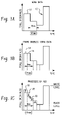
- FIGS. 1A-1C are diagrams depicting an alternating gamma drive (AGD) technique for reducing motion blur in an LCD.
- ATD alternating gamma drive
- FIG. 2A is a graph depicting example bright and dark gamma curves for AGD
- FIG. 2B is a graph depicting example look-up table (LUT) values for implementing the gamma curves.
- LUT look-up table
- FIG. 3 is a flow diagram depicting an example motion-adaptive AGD method for reducing motion blur in an LCD.
- FIG. 4 is a diagram depicting an example method for transitioning between AGD-ON and AGD-OFF modes.
- FIG. 5A is graph depicting example bright and dark gamma curves for AGD
- FIG. 5B is a graph that shows an example of how bright and dark LUT values may be modulated by coefficients to implement motion-adaptive AGD.
- FIG. 6 is a block diagram of an example motion-adaptive AGD system.
- FIG. 7 is a block diagram depicting another example motion-adaptive AGD system.
- FIG. 8 is a block diagram depicting an example system for detecting motion in a video signal.
- FIG. 9 depicts example motion detection patterns for the system of FIG. 8 .
- FIG. 10 is a block diagram depicting a further example of a motion-adaptive AGD system.
- FIGS. 11A-11E depict examples of various systems in which a motion-adaptive AGD system may be utilized.
- FIGS. 1A-1C illustrate an impulsive driving technique, referred to as alternating gamma drive (AGD), that may be used to reduce motion blur in an LCD.
- FIG. 1A shows an example 60 Hz video signal 10 for display on an LCD.
- LCDs are hold-type displays in which the same pixel brightness is maintained for the entire duration of the frame.
- the video signal 10 is first sampled at twice the frame rate (120 Hz), as shown in FIG. 1B .
- the pixel luminance is then varied in successive frames to provide an impulsive effect, as shown in FIG. 1C .
- the luminance is adjusted to achieve an impulsive effect in each set of frames that are not at the maximum (white) or minimum (black) brightness levels.
- the illustrated AGD technique implements an impulsive effect in the image by increasing and decreasing the brightness of successive frames such that the average luminance of adjacent frames preserves the original luminance of the image.
- An impulsive effect is achieved by increasing the luminance of the first 120 Hz frame 18 and decreasing the luminance of the second 120 Hz frame 20 , as shown in FIG. 1C .
- the average luminance 22 of the first and second gamma-adjusted 120 Hz frames 18 , 20 is the same as the luminance of the 60 Hz frame 12 .
- the human eye cannot perceive a difference between the original luminance of the 60 Hz frame 12 and the luminance in the first two gamma-adjusted 120 Hz frames 18 , 20 .
- FIG. 2A is a graph 30 depicting example bright and dark gamma curves 32 , 34 for implementing AGD.
- the middle gamma curve 36 represents the target gamma for the LCD.
- the bright and dark gamma curves 32 , 34 applied by the AGD technique are defined such that their average luminance corresponds to the target gamma 36 .
- the bright and dark gamma curves 32 , 34 may be achieved using look-up tables, as shown in FIG. 2B .
- FIG. 2B depicts example bright and dark look-up table values 40 , 42 that may be used to determine the amount by which the luminance of consecutive frames is increased or decreased during the AGD process.
- the look-up tables provide a light 40 and dark 42 delta value for adjusting the luminance to achieve an impulsive effect while maintaining the desired average gamma 36 .
- the light look-up table 40 may be used to determine the increase in luminance applied to the first gamma-corrected frame 18 based on the luminance value 22 of the original input data 12 .
- the dark look-up table 42 may be used to determine the decrease in luminance applied to the second gamma-corrected frame 20 .
- the AGD technique illustrated in FIGS. 1A-2B reduces LCD motion blur while maintaining the original luminance of the image.
- screen flicker may still pose a problem when displaying static images, particularly for image regions with mid-gray levels. This is because of a very large luminance change between frames.
- the image quality may be further degraded by quantization error of response time compensation (RTC) which typically uses interpolation technique for simple hardware.
- RTC response time compensation
- the quantization error in RTC calculation has nothing to do with image quality in case of conventional driving because RTC is applied only when images are in motion. Providing a higher accuracy RTC calculation typically leads to higher implementation costs. It has therefore been determined that a low-cost and high performance solution may be provided by utilizing a motion-adaptive AGD technique that selectively applies impulsive driving only for moving images.
- FIG. 3 is a flow diagram depicting an example motion-adaptive AGD method.
- step 50 incoming video frames are monitored to detect global motion. If motion is detected, then AGD is enabled in step 52 to reduce motion blur (referred to herein as AGD-ON mode). Otherwise, during periods when no motion is detected, AGD is disabled in step 54 to prevent screen flicker caused by applying AGD to still images (referred to herein as AGD-OFF mode).
- the AGD strength may be gradually transitioned during the mode switching phase, as illustrated in the example shown in FIG. 4 .
- the example depicted in FIG. 4 includes a first plot 60 that indicates periods during which motion is detected in an incoming video signal and a second plot 62 that shows the corresponding change in AGD strength.
- the AGD strength gradually rises or falls following a transition between AGD-ON and AGD-OFF modes.
- the minimum AGD strength shown in FIG. 4 corresponds to a gamma curve change of zero and the maximum AGD strength corresponds to the full amount of gamma curve modification. This is further illustrated with reference to the gamma correction curves shown in FIGS. 5A and 5B .
- FIG. 5A depicts example bright and dark gamma curves 70 , 72 for implementing AGD
- FIG. 5B depicts bright and dark look-up table values 74 , 76 for adjusting the luminance of consecutive frames to achieve the desired AGD gamma curves 70 , 72
- the top-most and bottom-most curves in FIG. 5B are the bright and dark look-up table values that are used at full AGD strength.
- the dotted curves depicted in FIG. 5B show the bright and dark luminance correction applied during the transitional periods shown in FIG. 4 to achieve a gradual increase or reduction in AGD strength.
- These transitional luminance correction values may, for example, be determined by applying a gain coefficient, C(m), to the bright and dark look-up table values 74 , 76 .
- a smooth transition is achieved by increasing C(m) in steps when motion is detected and decreasing C(m) in steps when motion stops.
- the step size for increasing and decreasing C(m), along with the duration of the transition period may be defined such that the human eye cannot perceive any luminance change.
- FIG. 6 is a block diagram of an example motion-adaptive AGD system 80 .
- the system 80 includes a frame-doubling data sampler 82 , a motion detection block 84 , a gain control block 86 , and bright (+Delta) and dark ( ⁇ Delta) lookup tables 88 , 90 . Also illustrated is a response time compensation (RTC) block 92 .
- RTC response time compensation
- the frame-doubling data sampler 82 receives an input video signal and re-samples the input at double speed (e.g., 120 Hz).
- the odd and even frames from the re-sampled video signal are then processed through two different data paths to implement motion-adaptive AGD.
- the motion detection block 84 monitors the incoming odd and even frames to detect motion in the received image.
- the motion detection block 84 may identify motion in the image by detecting changes in the pixel values between successive frames in the video input as a simplest implementation example.
- the motion detection block 84 generates a motion detection output to the gain control block 86 that indicates whether motion has been detected in the video input or whether the video image is still.
- the gain control block 86 generates a gain coefficient, for example as described above with reference to FIGS. 4-5B .
- the bright and dark look-up tables 88 , 90 are used to output luminance correction values ( ⁇ + and ⁇ ⁇ ) as a function of the luminance level of the re-sampled video signal.
- the luminance correction values ( ⁇ + and ⁇ ⁇ ) are multiplied by the gain coefficient and are then respectively applied to the odd and even frames of the re-sampled video signal to generate odd and even gamma-adjusted outputs (F odd and F even ).
- the gamma-adjusted outputs (F odd and F even ) are received by the RTC block 92 , which accelerates the temporal response time of the liquid crystal molecules of the LCD so that the luminance transition produced by the motion-adaptive AGD system 80 can occur within a single frame.
- FIG. 7 is a block diagram depicting another example motion-adaptive AGD system 100 .
- the re-sampled (frame-doubled) input is received by a motion detection and gain control block 102 .
- the motion detection and gain control block 102 includes motion detection logic that compares adjacent frames of the video input to determine how many pixels are changed. This value is then compared with a threshold value to identify motion in the image. The threshold value may be selected such that the motion detection logic will ignore small data changes that are not indicative of motion.
- the motion detection and gain control block 102 generates a gain control coefficient based on whether or not motion is detected in the video input, as described above.
- the gain control coefficient is applied to a luminance correction value from either a bright or dark look-up table 104 , 106 .
- the look-up tables 104 , 106 are selected using a frame selection circuit 108 that is controlled by a frame selection signal such that the gain-adjusted bright ( ⁇ + ) and dark ( ⁇ ⁇ ) luminance correction values are applied to alternating frames of the re-sampled data stream to generate a gamma-adjusted output.
- this example further includes a bypass circuit 110 that may be used to select either the gamma-corrected output or the unadjusted input as the video output (Data Out).
- FIG. 8 is a block diagram depicting an example system 120 for detecting motion in a video signal.
- the motion detection system 120 includes a frame comparison block 122 , a motion threshold comparison block 124 , an open-ended single bit shift register 126 and a pattern comparison block 128 .
- the motion-detection system 120 may, for example, be used to detect motion in the motion-adaptive AGD systems described herein with reference to FIGS. 6 , 7 and 10 .
- the motion detection system 120 compares adjacent frames 132 , 134 in a video signal to detect changes in the image that are indicative of motion.
- the frame comparison block 122 compares each pixel in the adjacent frames 132 , 134 to determine the total number of pixels that have changed.
- the frame comparison block 122 may utilize a pre-determined sensitivity setting 136 that provides a threshold value for identifying a change in an individual pixel value.
- the sensitivity setting 136 may be selected such that the frame comparison block 122 ignores slight pixel variations that may exist in a static image due to quantization error or noise between frames.
- the sensitivity setting 136 may be set to ignore the 2 LSB of each color (R, G, B) in a video frame with 24 BPP color depth. It should be understood, however, that other sensitivity settings 136 may also be utilized to achieve a desired sensitivity.
- the motion threshold comparison block 124 receives the total number of changed pixels from the frame comparison block 122 and compares this value with a programmable global motion threshold value.
- the motion threshold comparison block 124 generates a single bit output to the shift register 126 that indicates whether the total number of changed pixels is greater than the global motion threshold. For instance, the motion threshold comparison block 124 may output a “1” if the number of changed pixels is greater than the threshold and a “0” if it is not.
- the open-ended shift register 126 and the pattern comparison block 128 identify motion in the video signal when the pixel changes between frames remain greater than the global motion threshold for a pre-determined number of consecutive frames. Specifically, the pattern comparison block 128 compares the values stored in the open-ended shift register 126 with pre-determined ON and OFF patterns 138 , 140 to determine whether video images contain motion or are still. An example of ON and OFF patterns that may be utilized to detect motion are described below with reference to FIG. 9 .
- a feedback signal 142 may also be provided from the pattern comparison block 128 to the threshold comparison block 124 .
- the feedback signal 142 may be used to change the global motion detection threshold applied by the threshold comparison block 124 depending upon whether or not motion is detected. For instance, during periods when no motion is detected, a higher value global motion threshold may be used. The feedback signal 142 may then be used to lower the global motion threshold once motion has been detected. In this manner, once motion has initially been detected, less pixel change is needed to make a determination that the image remains in motion.
- the global motion threshold used in a static mode i.e., no motion detected
- the global motion threshold used in motion mode may be four times greater than the global motion threshold used in motion mode (i.e., after motion is initially detected); however, other ratios could also be used.
- FIG. 9 depicts example ON and OFF motion detection patterns 150 , 152 for the system of FIG. 8 .
- the example ON pattern 150 identifies motion in the video signal if the shift register 126 includes a “1” in any bit position within three consecutive three-bit windows 154 , 156 , 158 . That is, motion is identified if one or more logic level “1” is located in the shift register 126 at each of bit positions 1 - 3 , 4 - 6 and 7 - 9 .
- This example ON pattern 150 is used to account for the different bit patterns that will result during periods of motion depending upon the frame rates of the video source.
- Example bit patterns 160 - 162 indicative of motion are illustrated for frame rates of 24, 30 and 60 Hz, respectively. As illustrated, in each of these cases at least one logic level “1” will occur in each of the three windows 154 , 156 , 158 of the ON pattern 150 .
- the example OFF pattern 152 identifies that the video signal is not in motion upon detecting “0s” in nine consecutive bit positions of the shift register 126 .
- the OFF pattern 152 may be more simplistic than the ON pattern 150 because there is no frame rate dependency when the image is still.
- FIG. 10 is a block diagram depicting a further example of a motion-adaptive AGD system 200 .
- the system 200 includes a motion detection circuit 202 and a luminance control circuit 204 .
- a frame-doubled input 206 , 208 is received by both the motion detection circuit 202 and the luminance control circuit 204 .
- the motion detection circuit 202 identifies motion in the image by comparing the input frames 206 , 208 and generates a motion detection output (AGD ON/OFF) that indicates whether motion has been detected in the video input or whether the video image is still.
- AGD ON/OFF motion detection output
- the luminance control circuit 204 applies gain-adjusted bright and dark luminance correction values to the frame-doubled input 206 , 208 as a function of the motion detection output (AGD ON/OFF) such that AGD is applied to the frame-doubled input 206 , 208 only when motion has been detected by the motion detection circuit 202 .
- the motion detection circuit 202 in this example is similar to the motion detection circuit described above with reference to FIGS. 8 and 9 .
- the motion detection circuit 202 includes a comparison block 210 that compares each pixel in the adjacent frames 206 , 208 to determine the total number of pixels that have changed. This value is then compared with a global motion threshold value by a motion threshold comparison block 212 to generate a single bit output that is stored in an open-ended single bit shift register 214 .
- the stored values in the shift register 214 are compared to ON and OFF motion detection patterns by a pattern detection block 216 to determine whether the video images contain motion or are still.
- the pattern detection block 216 When motion is detected based on the ON pattern, the pattern detection block 216 generates an AGD ON output signal and also generates a threshold control signal to reduce the global motion threshold applied by the threshold detection block 212 . Similarly, when the images are determined to be still based on the OFF pattern, the pattern detection block 216 generates an AGD OFF output signal and also generates a threshold control signal to increase the global motion threshold.
- the luminance control circuit 204 includes an AGD gain control block 220 that generates a gain control coefficient based on the AGD ON/OFF output signal from the motion control circuit 202 .
- the gain control coefficient may, for example, be generated as described above with reference to FIGS. 4-5B .
- the gain control coefficient is applied to luminance correction values ( ⁇ + and ⁇ ⁇ ) that are respectively derived from bright and dark look-up tables 222 , 224 .
- the gain-corrected look-up table values are then added to the input frames 206 , 208 to generate odd and even gamma-adjusted outputs 226 , 228 .
- the present invention may be embodied in a high definition television (HDTV) 420 .
- the present invention may implement either or both signal processing and/or control circuits, which are generally identified in FIG. 11A at 422 , a WLAN interface and/or mass data storage of the HDTV 420 .
- HDTV 420 receives HDTV input signals in either a wired or wireless format and generates HDTV output signals for a display 426 .
- signal processing circuit and/or control circuit 422 and/or other circuits (not shown) of HDTV 420 may process data, perform coding and/or encryption, perform calculations, format data and/or perform any other type of HDTV processing that may be required.
- HDTV 420 may communicate with mass data storage 427 that stores data in a nonvolatile manner such as optical and/or magnetic storage devices.
- the HDD may be a mini HDD that includes one or more platters having a diameter that is smaller than approximately 1.8′′.
- HDTV 420 may be connected to memory 428 such as RAM, ROM, low latency nonvolatile memory such as flash memory and/or other suitable electronic data storage.
- HDTV 420 also may support connections with a WLAN via a WLAN network interface 429 .
- the present invention may be embodied in a cellular phone 450 that may include a cellular antenna 451 .
- the present invention may implement either or both signal processing and/or control circuits, which are generally identified in FIG. 11B at 452 , a WLAN interface and/or mass data storage of the cellular phone 450 .
- cellular phone 450 includes a microphone 456 , an audio output 458 such as a speaker and/or audio output jack, a display 460 and/or an input device 462 such as a keypad, pointing device, voice actuation and/or other input device.
- Signal processing and/or control circuits 452 and/or other circuits (not shown) in cellular phone 450 may process data, perform coding and/or encryption, perform calculations, format data and/or perform other cellular phone functions.
- Cellular phone 450 may communicate with mass data storage 464 that stores data in a nonvolatile manner such as optical and/or magnetic storage devices for example hard disk drives HDD and/or DVDs.
- the HDD may be a mini HDD that includes one or more platters having a diameter that is smaller than approximately 1.8′′.
- Cellular phone 450 may be connected to memory 466 such as RAM, ROM, low latency nonvolatile memory such as flash memory and/or other suitable electronic data storage.
- Cellular phone 450 also may support connections with a WLAN via a WLAN network interface 468 .
- the present invention may be embodied in a set top box 480 .
- the present invention may implement either or both signal processing and/or control circuits, which are generally identified in FIG. 11C at 484 , a WLAN interface and/or mass data storage of the set top box 480 .
- Set top box 480 receives signals from a source such as a broadband source and outputs standard and/or high definition audio/video signals suitable for a display 488 such as a television and/or monitor and/or other video and/or audio output devices.
- Signal processing and/or control circuits 484 and/or other circuits (not shown) of the set top box 480 may process data, perform coding and/or encryption, perform calculations, format data and/or perform any other set top box functions.
- Set top box 480 may communicate with mass data storage 490 that stores data in a nonvolatile manner.
- Mass data storage 490 may include optical and/or magnetic storage devices for example hard disk drives HDD and/or DVDs.
- the HDD may be a mini HDD that includes one or more platters having a diameter that is smaller than approximately 1.8′′.
- Set top box 480 may be connected to memory 494 such as RAM, ROM, low latency nonvolatile memory such as flash memory and/or other suitable electronic data storage.
- Set top box 480 also may support connections with a WLAN via a WLAN network interface 496 .
- the present invention may be embodied in a media player 500 .
- the present invention may implement either or both signal processing and/or control circuits, which are generally identified in FIG. 11D at 504 , a WLAN interface and/or mass data storage of the media player 500 .
- media player 500 includes a display 507 and/or a user input 508 such as a keypad, touchpad and the like.
- media player 500 may employ a graphical user interface (GUI) that typically employs menus, drop down menus, icons and/or a point-and-click interface via display 507 and/or user input 508 .
- Media player 500 further includes an audio output 509 such as a speaker and/or audio output jack.
- Signal processing and/or control circuits 504 and/or other circuits (not shown) of media player 500 may process data, perform coding and/or encryption, perform calculations, format data and/or perform any other media player function.
- Media player 500 may communicate with mass data storage 510 that stores data such as compressed audio and/or video content in a nonvolatile manner.
- the compressed audio files include files that are compliant with MP3 format or other suitable compressed audio and/or video formats.
- the mass data storage may include optical and/or magnetic storage devices for example hard disk drives HDD and/or DVDs.
- the HDD may be a mini HDD that includes one or more platters having a diameter that is smaller than approximately 1.8′′.
- Media player 500 may be connected to memory 514 such as RAM, ROM, low latency nonvolatile memory such as flash memory and/or other suitable electronic data storage.
- Media player 500 also may support connections with a WLAN via a WLAN network interface 516 . Still other implementations in addition to those described above are contemplated.
- VoIP phone 550 may include an antenna 518 .
- the present invention may implement either or both signal processing and/or control circuits, which are generally identified in FIG. 11E at 504 , a wireless interface and/or mass data storage of the VoIP phone 550 .
- VoIP phone 550 includes, in part, a microphone 510 , an audio output 512 such as a speaker and/or audio output jack, a display monitor 514 , an input device 516 such as a keypad, pointing device, voice actuation and/or other input devices, and a Wireless Fidelity (Wi-Fi) communication module 508 .
- Signal processing and/or control circuits 504 and/or other circuits (not shown) in VoIP phone 550 may process data, perform coding and/or encryption, perform calculations, format data and/or perform other VoIP phone functions.
- VoIP phone 550 may communicate with mass data storage 502 that stores data in a nonvolatile manner such as optical and/or magnetic storage devices, for example hard disk drives HDD and/or DVDs.
- the HDD may be a mini HDD that includes one or more platters having a diameter that is smaller than approximately 1.8′′.
- VoIP phone 550 may be connected to memory 506 , which may be a RAM, ROM, low latency nonvolatile memory such as flash memory and/or other suitable electronic data storage.
- VoIP phone 550 is configured to establish communications link with a VoIP network (not shown) via Wi-Fi communication module 508 .
Landscapes
- Engineering & Computer Science (AREA)
- Chemical & Material Sciences (AREA)
- Crystallography & Structural Chemistry (AREA)
- Physics & Mathematics (AREA)
- Computer Hardware Design (AREA)
- General Physics & Mathematics (AREA)
- Theoretical Computer Science (AREA)
- Liquid Crystal Display Device Control (AREA)
- Control Of Indicators Other Than Cathode Ray Tubes (AREA)
- Picture Signal Circuits (AREA)
Abstract
Description
AGD strength=|Δ++Δ−|,
where Δ+ is the increase in luminance from the input value and Δ− is the decrease in luminance from the input value. The AGD process can then be represented as follows:
D out,n =D in,n+(−1)n·Δ(d)
-
- where Δ(d)=Δ+, n=0, 2, 4, . . .
- Δ−, n=1, 3, 5, . . .
where n is frame number, d is the data value, and Δ is the gain value. To achieve a smooth transition scheme, the gain coefficient, C(m), may be introduced in accordance with the following equation:
D out,n =D in,n+(−1)n ·C(m)·Δ(d) - where Δ(d)=Δ+, n=0, 2, 4, . . .
- Δ−, n=1, 3, 5, . . .
Claims (38)
D out,n =D in,n+(−1)n ·C(m)·Δ(d),
D out,n =D in,n+(−1)n ·C(m)·Δ(d),
D out,n =D in,n+(−1)n ·C(m)·Δ(d),
D out,n =D in,n+(−1)n ·C(m)·Δ(d),
Priority Applications (1)
| Application Number | Priority Date | Filing Date | Title |
|---|---|---|---|
| US12/254,289 US8804048B2 (en) | 2007-10-25 | 2008-10-20 | Motion-adaptive alternate gamma drive for LCD |
Applications Claiming Priority (5)
| Application Number | Priority Date | Filing Date | Title |
|---|---|---|---|
| US98258007P | 2007-10-25 | 2007-10-25 | |
| US98646207P | 2007-11-08 | 2007-11-08 | |
| US98722807P | 2007-11-12 | 2007-11-12 | |
| US99147907P | 2007-11-30 | 2007-11-30 | |
| US12/254,289 US8804048B2 (en) | 2007-10-25 | 2008-10-20 | Motion-adaptive alternate gamma drive for LCD |
Publications (2)
| Publication Number | Publication Date |
|---|---|
| US20090109290A1 US20090109290A1 (en) | 2009-04-30 |
| US8804048B2 true US8804048B2 (en) | 2014-08-12 |
Family
ID=40229856
Family Applications (1)
| Application Number | Title | Priority Date | Filing Date |
|---|---|---|---|
| US12/254,289 Expired - Fee Related US8804048B2 (en) | 2007-10-25 | 2008-10-20 | Motion-adaptive alternate gamma drive for LCD |
Country Status (4)
| Country | Link |
|---|---|
| US (1) | US8804048B2 (en) |
| CN (1) | CN101868816B (en) |
| TW (1) | TWI450255B (en) |
| WO (1) | WO2009055328A2 (en) |
Families Citing this family (29)
| Publication number | Priority date | Publication date | Assignee | Title |
|---|---|---|---|---|
| US7952545B2 (en) * | 2006-04-06 | 2011-05-31 | Lockheed Martin Corporation | Compensation for display device flicker |
| TWI372377B (en) * | 2007-11-21 | 2012-09-11 | Mstar Semiconductor Inc | Method and apparatus for eliminating image blur by pixel-based processing |
| TW200926116A (en) * | 2007-12-03 | 2009-06-16 | Qisda Corp | Method of processing LCD images according to the content of the images |
| TWI386058B (en) * | 2008-10-03 | 2013-02-11 | Realtek Semiconductor Corp | Video processing method and device |
| JP5340083B2 (en) * | 2009-08-28 | 2013-11-13 | キヤノン株式会社 | Image display apparatus and brightness control method thereof |
| KR101630285B1 (en) * | 2009-10-28 | 2016-07-21 | 한화테크윈 주식회사 | Apparatus and method for color rolling suppression |
| JP5537121B2 (en) * | 2009-10-30 | 2014-07-02 | キヤノン株式会社 | Image processing apparatus and control method thereof |
| KR101094304B1 (en) * | 2010-02-23 | 2011-12-19 | 삼성모바일디스플레이주식회사 | Display device and image processing method |
| JP5381930B2 (en) * | 2010-08-20 | 2014-01-08 | 株式会社Jvcケンウッド | Video control apparatus and video control method |
| JP2012078590A (en) * | 2010-10-01 | 2012-04-19 | Canon Inc | Image display device and control method therefor |
| US9152872B2 (en) * | 2012-11-12 | 2015-10-06 | Accenture Global Services Limited | User experience analysis system to analyze events in a computer desktop |
| JP2014240913A (en) * | 2013-06-12 | 2014-12-25 | ソニー株式会社 | Display device and method for driving display device |
| CN103778897B (en) * | 2014-01-28 | 2016-03-02 | 北京京东方显示技术有限公司 | A kind of image display control method and device |
| JP6467865B2 (en) * | 2014-10-28 | 2019-02-13 | ソニー株式会社 | Image processing apparatus, camera system, image processing method, and program |
| US9658702B2 (en) * | 2015-08-12 | 2017-05-23 | Smart Technologies Ulc | System and method of object recognition for an interactive input system |
| US10325543B2 (en) * | 2015-12-15 | 2019-06-18 | a.u. Vista Inc. | Multi-mode multi-domain vertical alignment liquid crystal display and method thereof |
| CN107784981B (en) * | 2016-08-24 | 2020-08-04 | 联发科技股份有限公司 | Device applied to display and related image display method |
| JP2018063381A (en) * | 2016-10-14 | 2018-04-19 | 矢崎総業株式会社 | Display |
| CN108737825B (en) * | 2017-04-13 | 2023-05-02 | 腾讯科技(深圳)有限公司 | Video data coding method, device, computer equipment and storage medium |
| US11222606B2 (en) | 2017-12-19 | 2022-01-11 | Sony Group Corporation | Signal processing apparatus, signal processing method, and display apparatus |
| KR102757191B1 (en) * | 2019-11-27 | 2025-01-21 | 삼성전자주식회사 | Electronic device and method for controlling the same, and storage medium |
| EP3940586B1 (en) * | 2020-07-17 | 2025-09-17 | Sony Group Corporation | An electronic device and a related method for detecting and counting an action |
| US11495152B2 (en) * | 2020-09-01 | 2022-11-08 | Kostal Of America, Inc. | Method for diagnosing display connection and operation |
| CN112218156B (en) * | 2020-10-09 | 2022-07-29 | 海信视像科技股份有限公司 | Method for adjusting video dynamic contrast and display equipment |
| US11508273B2 (en) * | 2020-11-12 | 2022-11-22 | Synaptics Incorporated | Built-in test of a display driver |
| CN115914520A (en) * | 2021-09-30 | 2023-04-04 | 晶门科技(深圳)有限公司 | Dynamic motion detection method and device for display |
| EP4401418A1 (en) * | 2023-01-10 | 2024-07-17 | E-Peas | Device and method for automated output of an image motion area |
| KR20250132588A (en) * | 2024-02-28 | 2025-09-05 | 삼성디스플레이 주식회사 | Display apparatus and method of driving display panel using the same |
| CN121354505A (en) * | 2025-12-17 | 2026-01-16 | 福建亿林节能设备股份有限公司 | Multi-mode driven LCD display control system |
Citations (16)
| Publication number | Priority date | Publication date | Assignee | Title |
|---|---|---|---|---|
| US6288745B1 (en) * | 1997-04-24 | 2001-09-11 | Mitsubishi Denki Kabushiki Kaisha | Scanner line interpolation device |
| US20020136448A1 (en) * | 1998-07-20 | 2002-09-26 | Lau Technologies. | Real-time facial recognition and verification system |
| TW518555B (en) | 2000-04-21 | 2003-01-21 | Matsushita Electric Industrial Co Ltd | Gray-scale image display device that can reduce power consumption when writing data |
| US20030210256A1 (en) * | 2002-03-25 | 2003-11-13 | Yukio Mori | Display method and display apparatus |
| EP1536407A2 (en) | 2003-11-17 | 2005-06-01 | Sharp Kabushiki Kaisha | Image display apparatus, electronic apparatus, liquid crystal TV, liquid crystal driving apparatus, image display method, display control program and computer-readable recording medium |
| WO2006121188A1 (en) | 2005-05-11 | 2006-11-16 | Hitachi Displays, Ltd. | Display device |
| US20070035502A1 (en) * | 2005-08-10 | 2007-02-15 | Toshiba Matsushita Display Technology Co., Ltd. | Liquid crystal display device, method for controlling display data for liquid crystal display device, and recording media |
| US20070063944A1 (en) * | 2000-06-08 | 2007-03-22 | Ichiro Sato | Image display apparatus and image display method |
| WO2007040045A1 (en) | 2005-09-30 | 2007-04-12 | Sharp Kabushiki Kaisha | Image display device and method |
| US20070103418A1 (en) | 2005-11-09 | 2007-05-10 | Masahiro Ogino | Image displaying apparatus |
| US20070159530A1 (en) * | 2005-12-09 | 2007-07-12 | Lg Electronics Inc. | Method and apparatus for controlling output of a surveillance image |
| US20070171217A1 (en) * | 2006-01-20 | 2007-07-26 | Chin-Peng Tsai | Display device capable of compensating for luminance of environments |
| US20070216616A1 (en) * | 2004-06-01 | 2007-09-20 | Koninklijke Philips Electronics, N.V. | Display Device Comprising A Light Source |
| US20070262937A1 (en) * | 2006-05-09 | 2007-11-15 | Masahiro Take | Image display apparatus, control signal generating apparatus, image display control method, and computer program product |
| US20080123987A1 (en) * | 2006-11-29 | 2008-05-29 | Yun-Hung Shen | Method and apparatus for eliminating image blur |
| US8154628B2 (en) * | 2006-09-14 | 2012-04-10 | Mitsubishi Electric Corporation | Image processing apparatus and imaging apparatus and method |
Family Cites Families (2)
| Publication number | Priority date | Publication date | Assignee | Title |
|---|---|---|---|---|
| JP2006349952A (en) * | 2005-06-15 | 2006-12-28 | Sony Corp | Image display apparatus and method |
| TWI369665B (en) * | 2006-11-29 | 2012-08-01 | Mstar Semiconductor Inc | Method and apparatus for eliminating image blur |
-
2008
- 2008-10-20 CN CN200880117197.XA patent/CN101868816B/en not_active Expired - Fee Related
- 2008-10-20 WO PCT/US2008/080459 patent/WO2009055328A2/en not_active Ceased
- 2008-10-20 US US12/254,289 patent/US8804048B2/en not_active Expired - Fee Related
- 2008-10-23 TW TW097140735A patent/TWI450255B/en not_active IP Right Cessation
Patent Citations (17)
| Publication number | Priority date | Publication date | Assignee | Title |
|---|---|---|---|---|
| US6288745B1 (en) * | 1997-04-24 | 2001-09-11 | Mitsubishi Denki Kabushiki Kaisha | Scanner line interpolation device |
| US20020136448A1 (en) * | 1998-07-20 | 2002-09-26 | Lau Technologies. | Real-time facial recognition and verification system |
| TW518555B (en) | 2000-04-21 | 2003-01-21 | Matsushita Electric Industrial Co Ltd | Gray-scale image display device that can reduce power consumption when writing data |
| US20070063944A1 (en) * | 2000-06-08 | 2007-03-22 | Ichiro Sato | Image display apparatus and image display method |
| US20030210256A1 (en) * | 2002-03-25 | 2003-11-13 | Yukio Mori | Display method and display apparatus |
| EP1536407A2 (en) | 2003-11-17 | 2005-06-01 | Sharp Kabushiki Kaisha | Image display apparatus, electronic apparatus, liquid crystal TV, liquid crystal driving apparatus, image display method, display control program and computer-readable recording medium |
| US20070216616A1 (en) * | 2004-06-01 | 2007-09-20 | Koninklijke Philips Electronics, N.V. | Display Device Comprising A Light Source |
| WO2006121188A1 (en) | 2005-05-11 | 2006-11-16 | Hitachi Displays, Ltd. | Display device |
| US20070035502A1 (en) * | 2005-08-10 | 2007-02-15 | Toshiba Matsushita Display Technology Co., Ltd. | Liquid crystal display device, method for controlling display data for liquid crystal display device, and recording media |
| WO2007040045A1 (en) | 2005-09-30 | 2007-04-12 | Sharp Kabushiki Kaisha | Image display device and method |
| CN1975851A (en) | 2005-11-09 | 2007-06-06 | 株式会社日立显示器 | Image displaying apparatus |
| US20070103418A1 (en) | 2005-11-09 | 2007-05-10 | Masahiro Ogino | Image displaying apparatus |
| US20070159530A1 (en) * | 2005-12-09 | 2007-07-12 | Lg Electronics Inc. | Method and apparatus for controlling output of a surveillance image |
| US20070171217A1 (en) * | 2006-01-20 | 2007-07-26 | Chin-Peng Tsai | Display device capable of compensating for luminance of environments |
| US20070262937A1 (en) * | 2006-05-09 | 2007-11-15 | Masahiro Take | Image display apparatus, control signal generating apparatus, image display control method, and computer program product |
| US8154628B2 (en) * | 2006-09-14 | 2012-04-10 | Mitsubishi Electric Corporation | Image processing apparatus and imaging apparatus and method |
| US20080123987A1 (en) * | 2006-11-29 | 2008-05-29 | Yun-Hung Shen | Method and apparatus for eliminating image blur |
Non-Patent Citations (6)
| Title |
|---|
| European Patent Office, Invitation to Pay Additional Fees and Communication Relating to the Results of the Partial International Search, PCT/US2008/080459 issued Feb. 19, 2009. |
| First Office Action dated Feb. 8, 2014 from related/corresponding Taiwanese Patent Appl. No. 097140735. |
| Kimura, N. et al, "60.2: Invited Paper: New Technologies for Large-Sized High-Quality LCD TV", 2005 SID International Symposium, May 24, 2005, pp. 1734-1737, vol. XXXVI, SID International Symposium. |
| Notification of 2nd Office Action issued on Sep. 5, 2013 in related/corresponding Chinese Patent Application No. 200880117197.X. |
| Notification/Text of First Office Action issued in China dated Feb. 20, 2013 for related/corresponding Application No. 200880117197.X. |
| Third Office Action dated Jan. 2, 2014 from related/corresponding Chinese Patent Appl. No. 200880117197.X. |
Also Published As
| Publication number | Publication date |
|---|---|
| WO2009055328A2 (en) | 2009-04-30 |
| US20090109290A1 (en) | 2009-04-30 |
| TWI450255B (en) | 2014-08-21 |
| CN101868816A (en) | 2010-10-20 |
| CN101868816B (en) | 2014-06-18 |
| WO2009055328A3 (en) | 2010-01-21 |
| TW200931384A (en) | 2009-07-16 |
Similar Documents
| Publication | Publication Date | Title |
|---|---|---|
| US8804048B2 (en) | Motion-adaptive alternate gamma drive for LCD | |
| CN101764924B (en) | Method and apparatus for processing video data of liquid crystal display device | |
| US10199011B2 (en) | Generation of tone mapping function for dynamic pixel and backlight control | |
| JP5410731B2 (en) | Control method of backlight luminance suppression and display system using the control method | |
| EP1858257B1 (en) | Display device, contrast adjusting method and contrast adjusting program | |
| US20080238935A1 (en) | Contrast control apparatus and contrast control method and image display | |
| JP2008078858A (en) | Image display apparatus and method | |
| JP2004266755A (en) | Image processing device, image display device, and image processing method | |
| US8159567B2 (en) | Image processing apparatus and image processing method | |
| US8447131B2 (en) | Image processing apparatus and image processing method | |
| JP3602520B2 (en) | Liquid crystal display | |
| US20070164949A1 (en) | Device and method for driving liquid crystal display | |
| US8648784B2 (en) | Device and method for overdriving a liquid crystal display | |
| JP2009053221A (en) | Image display device and image display method | |
| JP2798169B2 (en) | Image display method and apparatus | |
| JP2006010839A (en) | Controller for display | |
| TW202331695A (en) | A method to display pixel design and control signal for lower power and higher bit depth | |
| JP4181612B2 (en) | Image display apparatus and method | |
| US7729022B2 (en) | Method for processing image | |
| US20120026185A1 (en) | Display apparatus and display method | |
| WO2024000181A1 (en) | Solid-state imaging device having tunable conversion gain, driving method, and electronic device | |
| KR101552886B1 (en) | Apparatus and method for improving picture quality of moving picture | |
| JP3785414B2 (en) | Liquid crystal display | |
| JP5132081B2 (en) | Display device | |
| JP6479401B2 (en) | Display device, control method of display device, and control program |
Legal Events
| Date | Code | Title | Description |
|---|---|---|---|
| AS | Assignment |
Owner name: MARVELL INTERNATIONAL LTD., BERMUDA Free format text: ASSIGNMENT OF ASSIGNORS INTEREST;ASSIGNOR:MARVELL SEMICONDUCTOR, INC.;REEL/FRAME:021737/0920 Effective date: 20081014 Owner name: MARVELL SEMICONDUCTOR, INC., CALIFORNIA Free format text: ASSIGNMENT OF ASSIGNORS INTEREST;ASSIGNORS:YE, BO;KIM, TAESUNG;VU, CHUNG PHAN;REEL/FRAME:021712/0603 Effective date: 20081014 Owner name: MARVELL INTERNATIONAL LTD., BERMUDA Free format text: LICENSE;ASSIGNOR:MARVELL WORLD TRADE LTD.;REEL/FRAME:021712/0675 Effective date: 20081015 Owner name: MARVELL WORLD TRADE LTD., BARBADOS Free format text: ASSIGNMENT OF ASSIGNORS INTEREST;ASSIGNOR:MARVELL INTERNATIONAL, LTD.;REEL/FRAME:021712/0662 Effective date: 20081015 |
|
| STCF | Information on status: patent grant |
Free format text: PATENTED CASE |
|
| AS | Assignment |
Owner name: MARVELL INTERNATIONAL LTD., BERMUDA Free format text: ASSIGNMENT OF ASSIGNORS INTEREST;ASSIGNOR:MARVELL WORLD TRADE LTD.;REEL/FRAME:043325/0124 Effective date: 20170608 |
|
| AS | Assignment |
Owner name: SYNAPTICS LLC, SWITZERLAND Free format text: ASSIGNMENT OF ASSIGNORS INTEREST;ASSIGNOR:MARVELL INTERNATIONAL LTD.;REEL/FRAME:043853/0827 Effective date: 20170611 Owner name: SYNAPTICS INCORPORATED, CALIFORNIA Free format text: ASSIGNMENT OF ASSIGNORS INTEREST;ASSIGNOR:MARVELL INTERNATIONAL LTD.;REEL/FRAME:043853/0827 Effective date: 20170611 |
|
| AS | Assignment |
Owner name: WELLS FARGO BANK, NATIONAL ASSOCIATION, NORTH CAROLINA Free format text: SECURITY INTEREST;ASSIGNOR:SYNAPTICS INCORPORATED;REEL/FRAME:044037/0896 Effective date: 20170927 Owner name: WELLS FARGO BANK, NATIONAL ASSOCIATION, NORTH CARO Free format text: SECURITY INTEREST;ASSIGNOR:SYNAPTICS INCORPORATED;REEL/FRAME:044037/0896 Effective date: 20170927 |
|
| MAFP | Maintenance fee payment |
Free format text: PAYMENT OF MAINTENANCE FEE, 4TH YEAR, LARGE ENTITY (ORIGINAL EVENT CODE: M1551) Year of fee payment: 4 |
|
| FEPP | Fee payment procedure |
Free format text: MAINTENANCE FEE REMINDER MAILED (ORIGINAL EVENT CODE: REM.); ENTITY STATUS OF PATENT OWNER: LARGE ENTITY |
|
| LAPS | Lapse for failure to pay maintenance fees |
Free format text: PATENT EXPIRED FOR FAILURE TO PAY MAINTENANCE FEES (ORIGINAL EVENT CODE: EXP.); ENTITY STATUS OF PATENT OWNER: LARGE ENTITY |
|
| STCH | Information on status: patent discontinuation |
Free format text: PATENT EXPIRED DUE TO NONPAYMENT OF MAINTENANCE FEES UNDER 37 CFR 1.362 |
|
| FP | Lapsed due to failure to pay maintenance fee |
Effective date: 20220812 |