US8779494B2 - High-k metal gate random access memory - Google Patents
High-k metal gate random access memory Download PDFInfo
- Publication number
- US8779494B2 US8779494B2 US13/426,825 US201213426825A US8779494B2 US 8779494 B2 US8779494 B2 US 8779494B2 US 201213426825 A US201213426825 A US 201213426825A US 8779494 B2 US8779494 B2 US 8779494B2
- Authority
- US
- United States
- Prior art keywords
- metal gate
- random access
- access memory
- units
- gate
- Prior art date
- Legal status (The legal status is an assumption and is not a legal conclusion. Google has not performed a legal analysis and makes no representation as to the accuracy of the status listed.)
- Active
Links
Images


Classifications
-
- H—ELECTRICITY
- H10—SEMICONDUCTOR DEVICES; ELECTRIC SOLID-STATE DEVICES NOT OTHERWISE PROVIDED FOR
- H10B—ELECTRONIC MEMORY DEVICES
- H10B12/00—Dynamic random access memory [DRAM] devices
- H10B12/01—Manufacture or treatment
- H10B12/02—Manufacture or treatment for one transistor one-capacitor [1T-1C] memory cells
- H10B12/05—Making the transistor
-
- H—ELECTRICITY
- H10—SEMICONDUCTOR DEVICES; ELECTRIC SOLID-STATE DEVICES NOT OTHERWISE PROVIDED FOR
- H10B—ELECTRONIC MEMORY DEVICES
- H10B12/00—Dynamic random access memory [DRAM] devices
- H10B12/30—DRAM devices comprising one-transistor - one-capacitor [1T-1C] memory cells
- H10B12/48—Data lines or contacts therefor
- H10B12/482—Bit lines
-
- H—ELECTRICITY
- H10—SEMICONDUCTOR DEVICES; ELECTRIC SOLID-STATE DEVICES NOT OTHERWISE PROVIDED FOR
- H10B—ELECTRONIC MEMORY DEVICES
- H10B12/00—Dynamic random access memory [DRAM] devices
- H10B12/30—DRAM devices comprising one-transistor - one-capacitor [1T-1C] memory cells
- H10B12/48—Data lines or contacts therefor
- H10B12/488—Word lines
Definitions
- the instant disclosure relates to a random access memory; in particular, to a high-k metal gate random access memory.
- DRAM dynamic random access memory
- the size reduction means higher storage density for the memory device.
- the internal channel length of the semiconductor components or the gaps in between the components has a decisive impact on component density and the critical dimension.
- the critical dimensions of the semiconductor components are limited by the manufacturing process. Taking the existing semiconductor manufacturing process for example, the critical factor that determines the dimensions of the semiconductor components is usually the minimum resolution of the photolithography process.
- the minimum resolution will continue to shrink as the semiconductor technology continues to advance.
- the semiconductor component can be downsized. The reason is during the downsizing process, the required physical and electrical properties of the semiconductor components may be lost due to excessive shrinkage.
- the internal channel of the semiconductor component may be too short.
- One of the consequences is the overlapping of the bit trapping regions, which can cause errors in reading and/or writing the data.
- leakage of electricity is more likely to occur for the semiconductor component.
- the capacitance for the capacitor of the memory device becomes more difficult to maintain, such that the stored data may be easily lost.
- the object of the instant disclosure is to provide a vertical high-k metal gate transistor, in particular a 4F2 DRAM to obtain a more capable memory device.
- the high-k metal gate random access memory of the instant disclosure comprises a substrate, a plurality of bit line units, a plurality of source regions, a plurality of gate structures, a plurality of drain regions, a plurality of word line units, and a plurality of capacitance units.
- the substrate has a plurality of upward extending trenches formed thereon.
- the bit line units and the trenches are alternately arranged on the substrate.
- Each of the source regions is formed on the respective bit line unit.
- Each of the gate structures is connected to the respective source region.
- Each gate structure is constructed of a metal gate and a channel area formed therein.
- the base surface of each drain region is in connection with the respective gate structure.
- the word line units are arranged between the source and drain regions to partially surround the periphery of the gate structures, and each capacitance unit is arranged on top of the respective drain region.
- the instant disclosure further discloses another high-k metal gate random access memory, which comprises: a substrate, a plurality of bit line units, a plurality of source regions, a plurality of gate structures, a plurality of drain regions, a plurality of word line units, and a plurality of capacitance units.
- the substrate has a plurality of upward extending trenches formed thereon.
- the bit line units and the trenches are alternately arranged on the substrate.
- Each of the source regions is formed on the respective bit line unit, and each of the gate structures is disposed on the respective source region.
- Each gate structure is constructed with a metal gate and a channel area is formed therein. Each channel area is bounded from the above by the respective drain region, where each drain region is formed inside the respective metal gate.
- the word line units are disposed in between the source regions and the drain regions.
- the word line units also partially surround the periphery of the gate structures.
- Each of the capacitance units has an upper electrode layer, a dielectric layer, and a lower electrode layer served by the respective drain region.
- the instant disclosure provides a vertical high-k metal gate transistor, in particular a 4F2 DRAM, where the drain regions, the gate structures, and the source regions are vertically arranged.
- the horizontal area of the transistor can be reduced to increase the component density, while maintaining the performance of the transistors.
- the high-k metal gate random access memory can reduce electricity leakage to enhance the electrical properties of the memory device.
- FIG. 1 shows a top view of a high-k metal gate random access memory of the instant disclosure.
- FIG. 2 shows a sectional view of the high-k metal gate random access memory in FIG. 1 taken along a cut-line AA′ for a first embodiment of the instant disclosure.
- FIG. 3 shows a sectional view of the high-k metal gate random access memory in FIG. 1 taken along a cut-line BB′ for the first embodiment of the instant disclosure.
- FIG. 4 shows a sectional view of the high-k metal gate random access memory in FIG. 1 taken along a cut-line CC′ for the first embodiment of the instant disclosure.
- FIG. 5 shows a sectional view of the high-k metal gate random access memory in FIG. 1 taken along a cut-line DD′ for the first embodiment of the instant disclosure.
- FIG. 6 shows a sectional view of a high-k metal gate random access memory in FIG. 1 taken along a cut-line AA′ for a second embodiment of the instant disclosure.
- FIG. 7 shows a sectional view of the high-k metal gate random access memory in FIG. 1 taken along a cut-line BB′ for the second embodiment of the instant disclosure.
- FIG. 8 shows a sectional view of the high-k metal gate random access memory in FIG. 1 taken along a cut-line CC′ for the second embodiment of the instant disclosure.
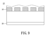
- FIG. 9 shows a sectional view of the high-k metal gate random access memory in FIG. 1 taken along a cut-line DD′ for the second embodiment of the instant disclosure.
- the instant disclosure provides a high-k metal gate random access memory 10 , which comprises a substrate 20 , a plurality of bit line units 30 , a plurality of source regions 41 , a plurality of gate structures 42 , a plurality of drain regions 45 , a plurality of word line units 50 , and a plurality of capacitance units 60 .
- FIG. 1 is a top view showing the structural layout of the high-k metal gate random access memory 10 .
- the layout is addressed by strip-type bit line units 30 arranged parallel at a distance from one another and word line units 50 which run transversely with respect to the bit line units 30 and likewise run parallel at a distance from one another.
- one capacitance unit 60 is disposed at each intersection between the bit line units 30 and the word line units 50 .
- FIG. 2 shows a sectional view of the random access memory 10 in FIG. 1 taken along a cut-line AA′ for a first embodiment of the instant disclosure.
- the substrate 20 has a plurality of trenches 21 formed thereon, where the trenches 21 extend beyond the substrate 20 .
- the trenches 21 are filled with insulating material such as silicon dioxide (silica), silicon nitride, borophosphosilicate glass (BPSG), phosphosilicate glass (PSG), undoped silicon glass (USG), or any material having high dielectric constant.
- the filler material is not restricted thereto.
- the bit line units 30 are arranged parallel at a distance from one another on the substrate 20 .
- the bit line units 30 and the trenches 21 are alternately arranged on the substrate 20 .
- a plurality of high-k metal gate transistors 40 is disposed on the bit line units 30 . Specially, the transistors 40 are perpendicular to the substrate 20 , unlike the conventional ones which are parallel.
- Each of the source regions 41 is disposed on the respective bit line unit 30 and separated from one another by the respective trench 21 .
- the source regions 41 are topped with gate structures 42 .
- the source regions 41 are made of polysilicons doped with n-type ions.
- Each of the gate structures 42 includes a metal gate 43 and a channel area 44 formed therein. More specially, the length of the channel area 44 is adjustable based on needs. In other words, the height of the gate structure 42 can be increased so that the length of the channel area 44 is also increased to reduce electricity leakage or improve electrical properties.
- the metal gate 43 can be made of titanium (Ti), titanium nitride (TiN), tantalum (Ta), tantalum nitride (TaN), tantalum carbide (TaC), tantalum silicide (TaSi 2 ), nickel silicide (NiSi 2 ), molybdenum silicide (MoSi 2 ), molybdenum nitride (MoN), tungsten (W), tungsten nitride (WN), or zirconium disilicide (ZrSi 2 ).
- the material used to construct the metal gate 43 is not restricted thereto.
- the channel area 44 is made of undoped polysilicon, polysilicon doped with ions, or any other high dielectric material.
- the channel area 44 is preferably made of undoped polysilicon.
- the other end of each gate structures 42 is connected to respective drain region 45 .
- the base surface of each drain region 45 is connected to the respective gate structure 42 .
- the drain region 45 is made of polysilicon doped with n-type ions.
- the word lines 50 are arranged between the source regions 41 and the drain regions 45 to partially surround the gate structures 42 . In others words, the gate structures 42 and the word lines 50 are alternately arranged. Furthermore, the capacitance units 60 are disposed on the drain regions 45 . Each of the capacitance units 60 includes an upper electrode layer 61 , a dielectric layer 62 , and lower electrode layer 63 . Specially, each capacitance unit 60 is connected to the respective drain region 45 through the lower electrode layer 63 . The upper electrode layer 61 is connected to a reference voltage.
- FIG. 3 where a sectional view of random access memory 10 of the first embodiment in FIG. 1 taken along a cut-line BB′ is shown.
- the bit line units 30 are parallel.
- the bit line units 30 and the trenches 21 are alternately arranged.
- FIG. 4 where a sectional view of the random access memory 10 in FIG. 1 taken along a cut-line CC′ is shown. Since the trenches 21 are alternately arranged with the transistors 40 along the longitudinal direction, the trenches 21 are not shown in FIG. 4 .
- FIG. 5 where a sectional view taken along a cut-line DD′ for the random access memory 10 in FIG. 1 is shown.
- the word lines 50 are parallel
- the instant disclosure further provides another high-k metal gate random access memory 10 .
- FIG. 6 where a sectional view of the random access memory 10 shown in FIG. 1 taken along the cut-line AA′ for the second embodiment is shown.
- each of the drain regions 45 and a portion of each gate structure 42 are arranged inside the respective capacitance unit 60 .
- the drain regions 45 are utilized as the lower electrode layers 63 of the capacitance units 60 .
- the dielectric layer 62 and the upper electrode layer 61 are formed correspondingly on the respective drain region 45 to form the capacitance unit 60 .
- Other physical structures of the random access memory 10 of the instant embodiment are identical to the previous embodiment, thus no further elaboration shall be provided herein.
- the metal gates 43 of the gate structures 42 of the instant embodiment cover the channel areas 44 and the drain regions 45 concurrently. Moreover, a portion of each metal gate 43 and a portion of each drain region 45 are extended inside the respective capacitance unit 60 to be in contact with the dielectric layer 62 . Since the drain regions 45 have the abilities to conduct electricity, the drain regions 45 are capable of being utilized as the lower electrode layers 63 of the capacitance units 60 . Specially, the length of the channel area 44 is adjustable based on needs so that the length of the channel area 44 is increased to reduce electricity leakage or improve electrical properties.
- FIG. 7 where a sectional view of the random access memory 10 in FIG. 1 taken along the cut-line BB′ for the second embodiment is shown.
- the bit line units 30 are parallel and alternately arranged with the trenches 21 .
- FIG. 8 where a sectional view of the random access memory 10 in FIG. 1 taken along the cut-line CC′ for the second embodiment is shown. Since the trenches 21 and the transistors 40 are alternately arranged along the longitudinal direction, the trenches 21 are not shown in the figure.
- FIG. 9 where a sectional view of the random access memory 10 in FIG. 1 taken along the cut-line DD′ for the second embodiment is shown.
- the word lines 50 are parallel.
- the present invention provides a vertical transistor, in particular to a 4F2 DRAM, where the drain regions, the gate structures, and the source regions are vertically arranged so that the lateral area of the transistor can be reduced.
- the component density can be increased while maintaining the performance of the transistors.
- the occurrence of electricity leakage can be reduced and the electrical properties of the random access memory can be improved.
Landscapes
- Engineering & Computer Science (AREA)
- Manufacturing & Machinery (AREA)
- Semiconductor Memories (AREA)
Abstract
Description
Claims (6)
Applications Claiming Priority (3)
| Application Number | Priority Date | Filing Date | Title |
|---|---|---|---|
| TW101100354A TWI488182B (en) | 2012-01-04 | 2012-01-04 | High-k metal gate random access memory |
| TW101100354A | 2012-01-04 | ||
| TW101100354 | 2012-01-04 |
Publications (2)
| Publication Number | Publication Date |
|---|---|
| US20130168751A1 US20130168751A1 (en) | 2013-07-04 |
| US8779494B2 true US8779494B2 (en) | 2014-07-15 |
Family
ID=48694146
Family Applications (1)
| Application Number | Title | Priority Date | Filing Date |
|---|---|---|---|
| US13/426,825 Active US8779494B2 (en) | 2012-01-04 | 2012-03-22 | High-k metal gate random access memory |
Country Status (2)
| Country | Link |
|---|---|
| US (1) | US8779494B2 (en) |
| TW (1) | TWI488182B (en) |
Families Citing this family (3)
| Publication number | Priority date | Publication date | Assignee | Title |
|---|---|---|---|---|
| CN112864098B (en) * | 2021-01-14 | 2023-06-30 | 长鑫存储技术有限公司 | Method for manufacturing semiconductor structure and semiconductor structure |
| US12096617B2 (en) | 2021-01-14 | 2024-09-17 | Changxin Memory Technologies, Inc. | Method of manufacturing semiconductor structure and semiconductor structure |
| CN113241347B (en) * | 2021-07-13 | 2021-10-15 | 芯盟科技有限公司 | Semiconductor structure and method for forming semiconductor structure |
Citations (4)
| Publication number | Priority date | Publication date | Assignee | Title |
|---|---|---|---|---|
| US20090189217A1 (en) * | 2004-11-08 | 2009-07-30 | Jae-Man Yoon | Semiconductor Memory Devices Including a Vertical Channel Transistor |
| US20090191677A1 (en) * | 2005-05-13 | 2009-07-30 | Micron Technology, Inc. | Memory array with surrounding gate access transistors and capacitors with global and staggered local bit lines |
| US20110042746A1 (en) * | 2006-11-01 | 2011-02-24 | Samsung Electronics Co., Ltd. | Single transistor memory device having source and drain insulating regions and method of fabricating the same |
| US20130069052A1 (en) * | 2011-09-16 | 2013-03-21 | Micron Technology, Inc. | Memory cells, semiconductor devices, systems including such cells, and methods of fabrication |
Family Cites Families (3)
| Publication number | Priority date | Publication date | Assignee | Title |
|---|---|---|---|---|
| US7271083B2 (en) * | 2004-07-22 | 2007-09-18 | Taiwan Semiconductor Manufacturing Company, Ltd. | One-transistor random access memory technology compatible with metal gate process |
| US8648403B2 (en) * | 2006-04-21 | 2014-02-11 | International Business Machines Corporation | Dynamic memory cell structures |
| US7826251B2 (en) * | 2008-05-22 | 2010-11-02 | International Business Machines Corporation | High performance metal gate polygate 8 transistor SRAM cell with reduced variability |
-
2012
- 2012-01-04 TW TW101100354A patent/TWI488182B/en active
- 2012-03-22 US US13/426,825 patent/US8779494B2/en active Active
Patent Citations (4)
| Publication number | Priority date | Publication date | Assignee | Title |
|---|---|---|---|---|
| US20090189217A1 (en) * | 2004-11-08 | 2009-07-30 | Jae-Man Yoon | Semiconductor Memory Devices Including a Vertical Channel Transistor |
| US20090191677A1 (en) * | 2005-05-13 | 2009-07-30 | Micron Technology, Inc. | Memory array with surrounding gate access transistors and capacitors with global and staggered local bit lines |
| US20110042746A1 (en) * | 2006-11-01 | 2011-02-24 | Samsung Electronics Co., Ltd. | Single transistor memory device having source and drain insulating regions and method of fabricating the same |
| US20130069052A1 (en) * | 2011-09-16 | 2013-03-21 | Micron Technology, Inc. | Memory cells, semiconductor devices, systems including such cells, and methods of fabrication |
Also Published As
| Publication number | Publication date |
|---|---|
| TW201329975A (en) | 2013-07-16 |
| US20130168751A1 (en) | 2013-07-04 |
| TWI488182B (en) | 2015-06-11 |
Similar Documents
| Publication | Publication Date | Title |
|---|---|---|
| US11646225B2 (en) | Semiconductor devices and methods of fabricating the same | |
| US10573653B2 (en) | Semiconductor devices having contact plugs overlapping associated bitline structures and contact holes | |
| US9548300B2 (en) | Semiconductor device including capacitor and method for manufacturing the same | |
| CN102709286B (en) | Isolation Structures and Component Structures Containing Isolation Structures | |
| US9064731B2 (en) | Semiconductor device having landing pads | |
| KR20220005866A (en) | Semiconductor dedvice | |
| KR20150068765A (en) | Semiconductor device and fabricating method thereof | |
| US20180158828A1 (en) | Semiconductor device including multi-liner layer in trench | |
| US10515977B2 (en) | Boundary design to reduce memory array edge CMP dishing effect | |
| CN110896073A (en) | Integrated circuit device including gate spacer structure | |
| CN110444543B (en) | Integrated assemblies containing carbon-doped oxides and methods of forming integrated assemblies | |
| US8946077B2 (en) | Method of manufacturing a semiconductor device | |
| US10461168B2 (en) | Semiconductor device for compensating internal delay, methods thereof, and data processing system having the same | |
| US8779494B2 (en) | High-k metal gate random access memory | |
| JP5283920B2 (en) | Semiconductor memory device | |
| US20150076612A1 (en) | Semiconductor Device | |
| TW202123388A (en) | Memory device | |
| US9548260B2 (en) | Semiconductor devices including conductive plug | |
| US9472495B2 (en) | Semiconductor device and method of manufacturing the same | |
| US9070740B2 (en) | Memory unit, memory unit array and method of manufacturing the same | |
| US20250185232A1 (en) | Semiconductor devices | |
| US20250169061A1 (en) | Semiconductor device | |
| US20230247822A1 (en) | Semiconductor device | |
| US20250071967A1 (en) | Semiconductor device | |
| US20250169076A1 (en) | Boundary design to reduce memory array edge cmp dishing effect |
Legal Events
| Date | Code | Title | Description |
|---|---|---|---|
| AS | Assignment |
Owner name: INOTERA MEMORIES, INC., TAIWAN Free format text: ASSIGNMENT OF ASSIGNORS INTEREST;ASSIGNORS:LEE, TZUNG-HAN;HUANG, CHUNG-LIN;CHU, RON FU;REEL/FRAME:027924/0100 Effective date: 20120322 |
|
| STCF | Information on status: patent grant |
Free format text: PATENTED CASE |
|
| AS | Assignment |
Owner name: MORGAN STANLEY SENIOR FUNDING, INC., MARYLAND Free format text: SUPPLEMENT NO. 3 TO PATENT SECURITY AGREEMENT;ASSIGNOR:MICRON TECHNOLOGY, INC.;REEL/FRAME:041675/0105 Effective date: 20170124 |
|
| AS | Assignment |
Owner name: MICRON TECHNOLOGY, INC., IDAHO Free format text: ASSIGNMENT OF ASSIGNORS INTEREST;ASSIGNOR:INOTERA MEMORIES, INC.;REEL/FRAME:041820/0815 Effective date: 20170222 |
|
| MAFP | Maintenance fee payment |
Free format text: PAYMENT OF MAINTENANCE FEE, 4TH YEAR, LARGE ENTITY (ORIGINAL EVENT CODE: M1551) Year of fee payment: 4 |
|
| AS | Assignment |
Owner name: JPMORGAN CHASE BANK, N.A., AS COLLATERAL AGENT, ILLINOIS Free format text: SECURITY INTEREST;ASSIGNORS:MICRON TECHNOLOGY, INC.;MICRON SEMICONDUCTOR PRODUCTS, INC.;REEL/FRAME:047540/0001 Effective date: 20180703 Owner name: JPMORGAN CHASE BANK, N.A., AS COLLATERAL AGENT, IL Free format text: SECURITY INTEREST;ASSIGNORS:MICRON TECHNOLOGY, INC.;MICRON SEMICONDUCTOR PRODUCTS, INC.;REEL/FRAME:047540/0001 Effective date: 20180703 |
|
| AS | Assignment |
Owner name: MICRON TECHNOLOGY, INC., IDAHO Free format text: RELEASE BY SECURED PARTY;ASSIGNOR:MORGAN STANLEY SENIOR FUNDING, INC., AS COLLATERAL AGENT;REEL/FRAME:050695/0825 Effective date: 20190731 |
|
| AS | Assignment |
Owner name: MICRON TECHNOLOGY, INC., IDAHO Free format text: RELEASE BY SECURED PARTY;ASSIGNOR:JPMORGAN CHASE BANK, N.A., AS COLLATERAL AGENT;REEL/FRAME:051028/0001 Effective date: 20190731 Owner name: MICRON SEMICONDUCTOR PRODUCTS, INC., IDAHO Free format text: RELEASE BY SECURED PARTY;ASSIGNOR:JPMORGAN CHASE BANK, N.A., AS COLLATERAL AGENT;REEL/FRAME:051028/0001 Effective date: 20190731 |
|
| MAFP | Maintenance fee payment |
Free format text: PAYMENT OF MAINTENANCE FEE, 8TH YEAR, LARGE ENTITY (ORIGINAL EVENT CODE: M1552); ENTITY STATUS OF PATENT OWNER: LARGE ENTITY Year of fee payment: 8 |
|
| MAFP | Maintenance fee payment |
Free format text: PAYMENT OF MAINTENANCE FEE, 12TH YEAR, LARGE ENTITY (ORIGINAL EVENT CODE: M1553); ENTITY STATUS OF PATENT OWNER: LARGE ENTITY Year of fee payment: 12 |