US8766378B2 - Programmable FETs using Vt-shift effect and methods of manufacture - Google Patents
Programmable FETs using Vt-shift effect and methods of manufacture Download PDFInfo
- Publication number
- US8766378B2 US8766378B2 US13/803,470 US201313803470A US8766378B2 US 8766378 B2 US8766378 B2 US 8766378B2 US 201313803470 A US201313803470 A US 201313803470A US 8766378 B2 US8766378 B2 US 8766378B2
- Authority
- US
- United States
- Prior art keywords
- tin
- metal
- metal gate
- design
- layer
- Prior art date
- Legal status (The legal status is an assumption and is not a legal conclusion. Google has not performed a legal analysis and makes no representation as to the accuracy of the status listed.)
- Expired - Fee Related
Links
- 230000000694 effects Effects 0.000 title claims abstract description 9
- 238000000034 method Methods 0.000 title abstract description 28
- 238000004519 manufacturing process Methods 0.000 title abstract description 21
- 229910052751 metal Inorganic materials 0.000 claims abstract description 71
- 239000002184 metal Substances 0.000 claims abstract description 71
- ATJFFYVFTNAWJD-UHFFFAOYSA-N Tin Chemical compound [Sn] ATJFFYVFTNAWJD-UHFFFAOYSA-N 0.000 claims description 25
- 239000000463 material Substances 0.000 claims description 19
- VYPSYNLAJGMNEJ-UHFFFAOYSA-N Silicium dioxide Chemical compound O=[Si]=O VYPSYNLAJGMNEJ-UHFFFAOYSA-N 0.000 claims description 10
- 229910052735 hafnium Inorganic materials 0.000 claims description 7
- VBJZVLUMGGDVMO-UHFFFAOYSA-N hafnium atom Chemical compound [Hf] VBJZVLUMGGDVMO-UHFFFAOYSA-N 0.000 claims description 7
- 239000012212 insulator Substances 0.000 claims description 7
- 239000003989 dielectric material Substances 0.000 claims description 6
- 229910021332 silicide Inorganic materials 0.000 claims description 6
- FVBUAEGBCNSCDD-UHFFFAOYSA-N silicide(4-) Chemical compound [Si-4] FVBUAEGBCNSCDD-UHFFFAOYSA-N 0.000 claims description 6
- 125000006850 spacer group Chemical group 0.000 claims description 6
- QVGXLLKOCUKJST-UHFFFAOYSA-N atomic oxygen Chemical compound [O] QVGXLLKOCUKJST-UHFFFAOYSA-N 0.000 claims description 5
- 229910052681 coesite Inorganic materials 0.000 claims description 5
- 229910052906 cristobalite Inorganic materials 0.000 claims description 5
- 229910052760 oxygen Inorganic materials 0.000 claims description 5
- 239000001301 oxygen Substances 0.000 claims description 5
- 239000000377 silicon dioxide Substances 0.000 claims description 5
- 229910052682 stishovite Inorganic materials 0.000 claims description 5
- 229910052905 tridymite Inorganic materials 0.000 claims description 5
- 230000005669 field effect Effects 0.000 abstract description 4
- 238000013461 design Methods 0.000 description 67
- 238000012938 design process Methods 0.000 description 15
- 238000012360 testing method Methods 0.000 description 10
- 238000005516 engineering process Methods 0.000 description 9
- 238000012545 processing Methods 0.000 description 8
- 238000004088 simulation Methods 0.000 description 8
- 230000008569 process Effects 0.000 description 7
- 239000004065 semiconductor Substances 0.000 description 6
- CJNBYAVZURUTKZ-UHFFFAOYSA-N hafnium(iv) oxide Chemical compound O=[Hf]=O CJNBYAVZURUTKZ-UHFFFAOYSA-N 0.000 description 5
- 238000003860 storage Methods 0.000 description 5
- 239000000758 substrate Substances 0.000 description 5
- IJGRMHOSHXDMSA-UHFFFAOYSA-N Atomic nitrogen Chemical compound N#N IJGRMHOSHXDMSA-UHFFFAOYSA-N 0.000 description 4
- 238000000137 annealing Methods 0.000 description 4
- 238000011960 computer-aided design Methods 0.000 description 4
- 230000005540 biological transmission Effects 0.000 description 3
- 238000013500 data storage Methods 0.000 description 3
- 238000000151 deposition Methods 0.000 description 3
- 238000010586 diagram Methods 0.000 description 3
- 238000012986 modification Methods 0.000 description 3
- 230000004048 modification Effects 0.000 description 3
- PXHVJJICTQNCMI-UHFFFAOYSA-N Nickel Chemical compound [Ni] PXHVJJICTQNCMI-UHFFFAOYSA-N 0.000 description 2
- 238000004458 analytical method Methods 0.000 description 2
- 239000007795 chemical reaction product Substances 0.000 description 2
- 238000005229 chemical vapour deposition Methods 0.000 description 2
- 238000005137 deposition process Methods 0.000 description 2
- 230000006870 function Effects 0.000 description 2
- WIHZLLGSGQNAGK-UHFFFAOYSA-N hafnium(4+);oxygen(2-) Chemical class [O-2].[O-2].[Hf+4] WIHZLLGSGQNAGK-UHFFFAOYSA-N 0.000 description 2
- 230000007246 mechanism Effects 0.000 description 2
- 229910021334 nickel silicide Inorganic materials 0.000 description 2
- RUFLMLWJRZAWLJ-UHFFFAOYSA-N nickel silicide Chemical compound [Ni]=[Si]=[Ni] RUFLMLWJRZAWLJ-UHFFFAOYSA-N 0.000 description 2
- 229910052757 nitrogen Inorganic materials 0.000 description 2
- 238000001020 plasma etching Methods 0.000 description 2
- 239000000047 product Substances 0.000 description 2
- 238000012795 verification Methods 0.000 description 2
- ZOXJGFHDIHLPTG-UHFFFAOYSA-N Boron Chemical compound [B] ZOXJGFHDIHLPTG-UHFFFAOYSA-N 0.000 description 1
- XUIMIQQOPSSXEZ-UHFFFAOYSA-N Silicon Chemical compound [Si] XUIMIQQOPSSXEZ-UHFFFAOYSA-N 0.000 description 1
- 238000009825 accumulation Methods 0.000 description 1
- 238000000277 atomic layer chemical vapour deposition Methods 0.000 description 1
- 230000015572 biosynthetic process Effects 0.000 description 1
- 229910052796 boron Inorganic materials 0.000 description 1
- 238000005266 casting Methods 0.000 description 1
- 230000015556 catabolic process Effects 0.000 description 1
- 239000000919 ceramic Substances 0.000 description 1
- 238000012512 characterization method Methods 0.000 description 1
- 238000004140 cleaning Methods 0.000 description 1
- 230000007812 deficiency Effects 0.000 description 1
- 238000006731 degradation reaction Methods 0.000 description 1
- 229910000449 hafnium oxide Inorganic materials 0.000 description 1
- 238000010438 heat treatment Methods 0.000 description 1
- 239000013067 intermediate product Substances 0.000 description 1
- 238000012804 iterative process Methods 0.000 description 1
- 238000001459 lithography Methods 0.000 description 1
- 238000000465 moulding Methods 0.000 description 1
- 230000006855 networking Effects 0.000 description 1
- 229910052759 nickel Inorganic materials 0.000 description 1
- 150000004767 nitrides Chemical class 0.000 description 1
- 230000003287 optical effect Effects 0.000 description 1
- 238000000059 patterning Methods 0.000 description 1
- 230000035515 penetration Effects 0.000 description 1
- 238000000623 plasma-assisted chemical vapour deposition Methods 0.000 description 1
- 238000009877 rendering Methods 0.000 description 1
- 229910052710 silicon Inorganic materials 0.000 description 1
- 239000010703 silicon Substances 0.000 description 1
- 238000004544 sputter deposition Methods 0.000 description 1
- 230000002194 synthesizing effect Effects 0.000 description 1
- 238000002076 thermal analysis method Methods 0.000 description 1
Images


Classifications
-
- H—ELECTRICITY
- H01—ELECTRIC ELEMENTS
- H01L—SEMICONDUCTOR DEVICES NOT COVERED BY CLASS H10
- H01L29/00—Semiconductor devices adapted for rectifying, amplifying, oscillating or switching, or capacitors or resistors with at least one potential-jump barrier or surface barrier, e.g. PN junction depletion layer or carrier concentration layer; Details of semiconductor bodies or of electrodes thereof ; Multistep manufacturing processes therefor
- H01L29/40—Electrodes ; Multistep manufacturing processes therefor
- H01L29/408—Electrodes ; Multistep manufacturing processes therefor with an insulating layer with a particular dielectric or electrostatic property, e.g. with static charges or for controlling trapped charges or moving ions, or with a plate acting on the insulator potential or the insulator charges, e.g. for controlling charges effect or potential distribution in the insulating layer, or with a semi-insulating layer contacting directly the semiconductor surface
-
- H—ELECTRICITY
- H01—ELECTRIC ELEMENTS
- H01L—SEMICONDUCTOR DEVICES NOT COVERED BY CLASS H10
- H01L21/00—Processes or apparatus adapted for the manufacture or treatment of semiconductor or solid state devices or of parts thereof
- H01L21/02—Manufacture or treatment of semiconductor devices or of parts thereof
- H01L21/04—Manufacture or treatment of semiconductor devices or of parts thereof the devices having at least one potential-jump barrier or surface barrier, e.g. PN junction, depletion layer or carrier concentration layer
- H01L21/18—Manufacture or treatment of semiconductor devices or of parts thereof the devices having at least one potential-jump barrier or surface barrier, e.g. PN junction, depletion layer or carrier concentration layer the devices having semiconductor bodies comprising elements of Group IV of the Periodic System or AIIIBV compounds with or without impurities, e.g. doping materials
- H01L21/28—Manufacture of electrodes on semiconductor bodies using processes or apparatus not provided for in groups H01L21/20 - H01L21/268
- H01L21/28008—Making conductor-insulator-semiconductor electrodes
- H01L21/28017—Making conductor-insulator-semiconductor electrodes the insulator being formed after the semiconductor body, the semiconductor being silicon
- H01L21/28026—Making conductor-insulator-semiconductor electrodes the insulator being formed after the semiconductor body, the semiconductor being silicon characterised by the conductor
- H01L21/28088—Making conductor-insulator-semiconductor electrodes the insulator being formed after the semiconductor body, the semiconductor being silicon characterised by the conductor the final conductor layer next to the insulator being a composite, e.g. TiN
-
- G—PHYSICS
- G06—COMPUTING; CALCULATING OR COUNTING
- G06F—ELECTRIC DIGITAL DATA PROCESSING
- G06F30/00—Computer-aided design [CAD]
- G06F30/30—Circuit design
-
- H—ELECTRICITY
- H01—ELECTRIC ELEMENTS
- H01L—SEMICONDUCTOR DEVICES NOT COVERED BY CLASS H10
- H01L21/00—Processes or apparatus adapted for the manufacture or treatment of semiconductor or solid state devices or of parts thereof
- H01L21/02—Manufacture or treatment of semiconductor devices or of parts thereof
- H01L21/04—Manufacture or treatment of semiconductor devices or of parts thereof the devices having at least one potential-jump barrier or surface barrier, e.g. PN junction, depletion layer or carrier concentration layer
- H01L21/18—Manufacture or treatment of semiconductor devices or of parts thereof the devices having at least one potential-jump barrier or surface barrier, e.g. PN junction, depletion layer or carrier concentration layer the devices having semiconductor bodies comprising elements of Group IV of the Periodic System or AIIIBV compounds with or without impurities, e.g. doping materials
- H01L21/28—Manufacture of electrodes on semiconductor bodies using processes or apparatus not provided for in groups H01L21/20 - H01L21/268
- H01L21/28008—Making conductor-insulator-semiconductor electrodes
- H01L21/28017—Making conductor-insulator-semiconductor electrodes the insulator being formed after the semiconductor body, the semiconductor being silicon
- H01L21/28158—Making the insulator
- H01L21/28167—Making the insulator on single crystalline silicon, e.g. using a liquid, i.e. chemical oxidation
- H01L21/28176—Making the insulator on single crystalline silicon, e.g. using a liquid, i.e. chemical oxidation with a treatment, e.g. annealing, after the formation of the definitive gate conductor
-
- H—ELECTRICITY
- H01—ELECTRIC ELEMENTS
- H01L—SEMICONDUCTOR DEVICES NOT COVERED BY CLASS H10
- H01L21/00—Processes or apparatus adapted for the manufacture or treatment of semiconductor or solid state devices or of parts thereof
- H01L21/02—Manufacture or treatment of semiconductor devices or of parts thereof
- H01L21/04—Manufacture or treatment of semiconductor devices or of parts thereof the devices having at least one potential-jump barrier or surface barrier, e.g. PN junction, depletion layer or carrier concentration layer
- H01L21/18—Manufacture or treatment of semiconductor devices or of parts thereof the devices having at least one potential-jump barrier or surface barrier, e.g. PN junction, depletion layer or carrier concentration layer the devices having semiconductor bodies comprising elements of Group IV of the Periodic System or AIIIBV compounds with or without impurities, e.g. doping materials
- H01L21/28—Manufacture of electrodes on semiconductor bodies using processes or apparatus not provided for in groups H01L21/20 - H01L21/268
- H01L21/28008—Making conductor-insulator-semiconductor electrodes
- H01L21/28017—Making conductor-insulator-semiconductor electrodes the insulator being formed after the semiconductor body, the semiconductor being silicon
- H01L21/28158—Making the insulator
- H01L21/28167—Making the insulator on single crystalline silicon, e.g. using a liquid, i.e. chemical oxidation
- H01L21/28185—Making the insulator on single crystalline silicon, e.g. using a liquid, i.e. chemical oxidation with a treatment, e.g. annealing, after the formation of the gate insulator and before the formation of the definitive gate conductor
-
- H—ELECTRICITY
- H01—ELECTRIC ELEMENTS
- H01L—SEMICONDUCTOR DEVICES NOT COVERED BY CLASS H10
- H01L21/00—Processes or apparatus adapted for the manufacture or treatment of semiconductor or solid state devices or of parts thereof
- H01L21/02—Manufacture or treatment of semiconductor devices or of parts thereof
- H01L21/04—Manufacture or treatment of semiconductor devices or of parts thereof the devices having at least one potential-jump barrier or surface barrier, e.g. PN junction, depletion layer or carrier concentration layer
- H01L21/18—Manufacture or treatment of semiconductor devices or of parts thereof the devices having at least one potential-jump barrier or surface barrier, e.g. PN junction, depletion layer or carrier concentration layer the devices having semiconductor bodies comprising elements of Group IV of the Periodic System or AIIIBV compounds with or without impurities, e.g. doping materials
- H01L21/30—Treatment of semiconductor bodies using processes or apparatus not provided for in groups H01L21/20 - H01L21/26
- H01L21/324—Thermal treatment for modifying the properties of semiconductor bodies, e.g. annealing, sintering
-
- H—ELECTRICITY
- H01—ELECTRIC ELEMENTS
- H01L—SEMICONDUCTOR DEVICES NOT COVERED BY CLASS H10
- H01L29/00—Semiconductor devices adapted for rectifying, amplifying, oscillating or switching, or capacitors or resistors with at least one potential-jump barrier or surface barrier, e.g. PN junction depletion layer or carrier concentration layer; Details of semiconductor bodies or of electrodes thereof ; Multistep manufacturing processes therefor
- H01L29/40—Electrodes ; Multistep manufacturing processes therefor
- H01L29/43—Electrodes ; Multistep manufacturing processes therefor characterised by the materials of which they are formed
- H01L29/49—Metal-insulator-semiconductor electrodes, e.g. gates of MOSFET
- H01L29/4966—Metal-insulator-semiconductor electrodes, e.g. gates of MOSFET the conductor material next to the insulator being a composite material, e.g. organic material, TiN, MoSi2
-
- H—ELECTRICITY
- H01—ELECTRIC ELEMENTS
- H01L—SEMICONDUCTOR DEVICES NOT COVERED BY CLASS H10
- H01L29/00—Semiconductor devices adapted for rectifying, amplifying, oscillating or switching, or capacitors or resistors with at least one potential-jump barrier or surface barrier, e.g. PN junction depletion layer or carrier concentration layer; Details of semiconductor bodies or of electrodes thereof ; Multistep manufacturing processes therefor
- H01L29/40—Electrodes ; Multistep manufacturing processes therefor
- H01L29/43—Electrodes ; Multistep manufacturing processes therefor characterised by the materials of which they are formed
- H01L29/49—Metal-insulator-semiconductor electrodes, e.g. gates of MOSFET
- H01L29/51—Insulating materials associated therewith
- H01L29/517—Insulating materials associated therewith the insulating material comprising a metallic compound, e.g. metal oxide, metal silicate
-
- H—ELECTRICITY
- H01—ELECTRIC ELEMENTS
- H01L—SEMICONDUCTOR DEVICES NOT COVERED BY CLASS H10
- H01L29/00—Semiconductor devices adapted for rectifying, amplifying, oscillating or switching, or capacitors or resistors with at least one potential-jump barrier or surface barrier, e.g. PN junction depletion layer or carrier concentration layer; Details of semiconductor bodies or of electrodes thereof ; Multistep manufacturing processes therefor
- H01L29/66—Types of semiconductor device ; Multistep manufacturing processes therefor
- H01L29/68—Types of semiconductor device ; Multistep manufacturing processes therefor controllable by only the electric current supplied, or only the electric potential applied, to an electrode which does not carry the current to be rectified, amplified or switched
- H01L29/76—Unipolar devices, e.g. field effect transistors
- H01L29/772—Field effect transistors
- H01L29/78—Field effect transistors with field effect produced by an insulated gate
- H01L29/7833—Field effect transistors with field effect produced by an insulated gate with lightly doped drain or source extension, e.g. LDD MOSFET's; DDD MOSFET's
-
- H—ELECTRICITY
- H01—ELECTRIC ELEMENTS
- H01L—SEMICONDUCTOR DEVICES NOT COVERED BY CLASS H10
- H01L29/00—Semiconductor devices adapted for rectifying, amplifying, oscillating or switching, or capacitors or resistors with at least one potential-jump barrier or surface barrier, e.g. PN junction depletion layer or carrier concentration layer; Details of semiconductor bodies or of electrodes thereof ; Multistep manufacturing processes therefor
- H01L29/40—Electrodes ; Multistep manufacturing processes therefor
- H01L29/43—Electrodes ; Multistep manufacturing processes therefor characterised by the materials of which they are formed
- H01L29/49—Metal-insulator-semiconductor electrodes, e.g. gates of MOSFET
- H01L29/51—Insulating materials associated therewith
- H01L29/511—Insulating materials associated therewith with a compositional variation, e.g. multilayer structures
- H01L29/513—Insulating materials associated therewith with a compositional variation, e.g. multilayer structures the variation being perpendicular to the channel plane
Definitions
- the invention relates to semiconductor structures and methods of manufacture and, more particularly, to programmable field effect transistors (FETs) using high-k dielectric metal gate Vt shift effect and methods of manufacturing the same.
- FETs field effect transistors
- Negative Bias Temperature Instability is a key reliability issue that is of immediate concern in p-channel MOS devices operating with negative gate voltages. This same mechanism also affects nMOS transistors when biased in the accumulation regime, i.e., with a negative bias applied to the gate. NBTI manifests as an increase in the threshold voltage and consequent decrease in drain current and transconductance. The degradation exhibits log law dependence with time.
- Vt-shift by oxygen-ingress is an issue causing Vt variation in high-k dielectric metal gate technology. It is believed that the Vt shift is due to two components: stable component and meta-stable component.
- the stable component refers to the removal of oxygen vacancies in HfO 2 and the meta-stable component refers to the formation of oxygen interstitials in HfO 2 .
- a method of controlling Vt shift in a high-k dielectric metal gate structure comprises applying a current to a gate contact of the high-k dielectric metal gate structure to raise a temperature of a metal forming a gate stack. The temperature is raised beyond a temperature needed fro oxygen induced Vt shift on high-k materials.
- a method of controlling Vt shift in a TiN metal gate structure with a hafnium based dielectric comprises raising a temperature of the TiN metal to above a Vt shift threshold by applying a current through contacts of the TiN metal gate structure.
- a structure comprises a metal gate structure comprising a Ti based metal formed on a hafnium based dielectric material and a poly material formed on the Ti based metal.
- the Ti based metal exhibits a Vt shift control effect due to a current induced temperature increase.
- a method in a computer-aided design system for generating a functional design model of a programmable field effect transistor comprises generating a functional representation of a metal gate structure comprising a Ti based metal formed on a hafnium based dielectric material and a poly material formed on the Ti based metal.
- the Ti based metal exhibits a Vt shift control effect due to a current induced temperature increase.
- a design structure tangibly embodied in a machine readable storage medium for designing, manufacturing, or testing an integrated circuit comprises the structures of the present invention.
- a hardware description language (HDL) design structure encoded on a machine-readable data storage medium comprises elements that when processed in a computer-aided design system generates a machine-executable representation of the programmable FET, which comprises the structures of the present invention.
- a method in a computer-aided design system is provided for generating a functional design model of the programmable FET. The method comprises generating a functional representation of the structural elements of the programmable FET.
- FIGS. 1-6 show structures and respective processing steps in accordance with aspects of the invention
- FIG. 7 shows a graph of threshold voltage shift (Vt shift) vs. temperature
- FIG. 8 shows flatband voltage vs. annealing temperature
- FIG. 9 is a flow diagram of a design process used in semiconductor design, manufacture, and/or test.
- the invention relates to semiconductor structures and methods of manufacture and, more particularly, to programmable field effect transistors (FETs) with high-k dielectric metal gate Vt shift effect and methods of manufacturing the same.
- FETs field effect transistors
- the present invention provides a structure and fabrication methodology that uses a control effect to make programmable logic FET cells.
- the structure and fabrication methodology prevents Vt-shift by oxygen-ingress which causes Vt variation in high-k dielectric metal gate technologies.
- the present invention controls Vt-shift by gate current heating.
- This methodology improves yield and cost of masks for different Vt shifts, is flexible for all circuit designs, and has memory applications (e.g., multi-valued memory like mirrorbit, or write-once memory).
- the methodology and resulting structure is compatible and easier (compared to known methodologies) to apply on the state-of-the-art CMOS SOI high-k dielectric metal gate technologies (e.g., high performance, high density).
- the present invention can be implemented in many different applications such as, for example, a field-programmable gate array (FPGA).
- FPGA field-programmable gate array
- FIG. 1 shows a beginning structure and respective processing steps in accordance with aspects of the invention.
- the beginning structure 10 includes a substrate 12 .
- the substrate 12 can be, for example, SOI, BULK, Si or other known substrates used in the fabrication of semiconductor devices.
- a dielectric 14 is formed on the substrate 12 .
- the dielectric 14 is a high-k dielectric and can be, for example, a hafnium based material such as, hafnium dioxide (HfO 2 ); although other hafnium based dielectric materials are also contemplated by the present invention.
- the high-k dielectric can be HFSIO, or a stack of combinations of such materials with or without oxide materials.
- the dielectric 14 can be deposited to a thickness of about 10 ⁇ to about 20 ⁇ ; although other dimensions are contemplated by the present invention depending on design parameters and technology node.
- the dielectric 14 can be deposited using any well known deposition process such as, for example, chemical vapor deposition (CVD), ALCVD or PECVD.
- CVD chemical vapor deposition
- ALCVD ALCVD
- PECVD PECVD
- a metal 16 is formed on the dielectric 14 .
- the metal 16 can be one or more metal layers, depending on the particular design parameters.
- the metal 16 is Ti or TiN, which preferably responds well to the control effect of the present invention.
- the metal 16 can be deposited using conventional deposition methods as noted above, in addition to sputtering techniques.
- the metal 16 can be deposited to a thickness of about 20 ⁇ to about 40 ⁇ ; although other dimensions are contemplated by the present invention depending on design parameters, technology node and preferences related to controlling the Vt shift using the methodologies described herein.
- a poly layer 18 is deposited on the metal 16 using conventional deposition methods as noted above.
- the poly layer 18 can be deposited to a thickness of about 400 ⁇ to about 500 ⁇ ; although other dimensions are contemplated by the present invention depending on design parameters and technology node.
- the dielectric 14 , metal 16 and poly layer 18 undergo a patterning process to form a metal gate stack 20 .
- a resist can be deposited on the poly layer 18 , masked and exposed to light to form a pattern. Once the exposed resist is washed away, a conventional reactive ion etching (RIE) can be used to form the metal gate stack 20 .
- RIE reactive ion etching
- a sidewall spacer 22 can be formed using conventional deposition processes, as noted above.
- the sidewall spacer 22 is a SiO 2 ; although other materials such as nitride can also be used as the sidewall spacer 22 .
- an optional layer 24 is deposited on the top of the metal gate stack 20 and the sidewall spacers 22 .
- the optional layer 24 is SiN.
- the optional layer 24 can be deposited using the conventional deposition methods noted above.
- a metal is deposited on the sides of the optional layer 24 on the substrate 12 .
- the metal is preferably a nickel layer which is then annealed to form nickel silicide contact regions 26 .
- the annealing is performed at about 400° C., which is a temperature that will not melt the metal 16 .
- the nickel silicide contact regions 26 will act as a contact region for source and drain regions.
- the metal can also be deposited on top of the metal gate stack 20 to form a contact region for the metal gate stack. (See, e.g., FIG. 7 ).
- an insulator layer 28 is deposited on the structure.
- the insulator layer 28 may be, for example, a SiO 2 ; although other insulator materials are also contemplated by the present invention.
- a wiring layer or contact 30 is formed in the insulator layer 28 to the silicide contact regions 26 .
- a trench or via (opening) is opened in the insulator layer 30 to the silicide contact regions 26 on the source and drain regions and the metal gate stack using conventional lithographic fabrication processes.
- a metal is then deposited in the openings to form contacts or wirings 30 in electrical and direct contact with the silicide contact regions 26 .
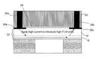
- FIG. 6 is a cross sectional view along line A-A of FIG. 5 , showing the contacts or wirings 30 directly and electrically contacting the silicide contact regions 26 of the metal gate stack 20 . More specifically, as shown in FIG. 6 , a current is applied through the contacts or wirings 30 directly and electrically contacting the silicide contact regions 26 of the metal gate stack 20 . The current is passed through the poly layer 18 and into the metal layer 16 , and back into the poly layer 18 and to the other of the contacts or wirings 30 b of the metal gate stack 20 . The high current introduces a high temperature and hence heats the metal 16 which, in turn, induces a Vt shift in the gate metal 16 . In embodiments, 1.2 voltage can raise the temperature of the TiN metal 16 to about at least about 625° C. and preferably about 900° C. or greater, depending on the thickness and other dimensions of the metal gate material.
- the thermal conductivity of the metal gate material is about 40 W/(M ⁇ K). Assuming the TiN layer is 0.4 um wide, 0.04 um thick and 0.04 um long, the thermal resistance of the TiN is about 6.25 ⁇ 10 4 K/W. Also, in this example, the power dissipation is about 1 ⁇ 10 ⁇ 2 W.
- the temperature delta is about 625° C., which is much higher than the temperature needed for oxygen induced Vt shift on high-K materials.
- R hs is the thermal resistance of Si/SiO 2 .
- P th is the thermal power
- R s is the thermal resistance of the TiN
- ⁇ T is the temperature difference
- Si/SiO 2 thermal resistance is much smaller than TiN.
- the dimensions of the TiN metal 16
- the dimensions of the TiN will affect the temperature rise and required applied voltage to provide the Vt shift in accordance with the present invention.
- one of skill in the art can easily determine the preferred dimensions of the TiN for the required Vt shift (without further explanation).
- FIG. 7 shows a graph of threshold voltage shift (Vt shift) vs. temperature.
- Vt shift threshold voltage shift
- the graph of FIG. 7 shows that a low temperature anneal of about 400° C. to about 600° C. will result in a Vt shift to high, e.g., an off state. With this temperature rise, the device will shut off an not conduct. However, a high temperature anneal of greater than 600° C. will begin shifting the Vt to low.
- a temperature increase of about greater than 900° C. will result in Vt shift to low, e.g., an on state. With this temperature rise, the device will be “on” and conduct. Accordingly, by providing a current to the device as discussed with reference to FIG. 6 , e.g., 1 voltage raises the temperature to about 900° C., it is possible to provide a Vt shift of the device to the “on” state.
- FIG. 8 shows flatband voltage vs. annealing temperature.
- FIG. 8 shows a programmable Vt shift by using a temperature increase in the device. Accordingly, it is possible by providing a current to the device as discussed with reference to FIG. 1 , that the device can be Vt shifted. In this graphical representation, a large Vt shift begins to occur at about 500° C.
- FIG. 9 is a flow diagram of a design process used in semiconductor design, manufacture, and/or test.
- FIG. 9 shows a block diagram of an exemplary design flow 900 used for example, in semiconductor IC logic design, simulation, test, layout, and manufacture.
- Design flow 900 includes processes, machines and/or mechanisms for processing design structures or devices to generate logically or otherwise functionally equivalent representations of the design structures and/or devices described above and shown in FIGS. 1-6 .
- the design structures processed and/or generated by design flow 900 may be encoded on machine-readable transmission or storage media to include data and/or instructions that when executed or otherwise processed on a data processing system generate a logically, structurally, mechanically, or otherwise functionally equivalent representation of hardware components, circuits, devices, or systems.
- Machines include, but are not limited to, any machine used in an IC design process, such as designing, manufacturing, or simulating a circuit, component, device, or system.
- machines may include: lithography machines, machines and/or equipment for generating masks (e.g. e-beam writers), computers or equipment for simulating design structures, any apparatus used in the manufacturing or test process, or any machines for programming functionally equivalent representations of the design structures into any medium (e.g. a machine for programming a programmable gate array).
- Design flow 900 may vary depending on the type of representation being designed. For example, a design flow 900 for building an application specific IC (ASIC) may differ from a design flow 900 for designing a standard component or from a design flow 900 for instantiating the design into a programmable array, for example a programmable gate array (PGA) or a field programmable gate array (FPGA) offered by Altera® Inc. or Xilinx® Inc.
- ASIC application specific IC
- PGA programmable gate array
- FPGA field programmable gate array
- FIG. 9 illustrates multiple such design structures including an input design structure 920 that is preferably processed by a design process 910 .
- Design structure 920 may be a logical simulation design structure generated and processed by design process 910 to produce a logically equivalent functional representation of a hardware device.
- Design structure 920 may also or alternatively comprise data and/or program instructions that when processed by design process 910 , generate a functional representation of the physical structure of a hardware device. Whether representing functional and/or structural design features, design structure 920 may be generated using electronic computer-aided design (ECAD) such as implemented by a core developer/designer.
- ECAD electronic computer-aided design
- design structure 920 When encoded on a machine-readable data transmission, gate array, or storage medium, design structure 920 may be accessed and processed by one or more hardware and/or software modules within design process 910 to simulate or otherwise functionally represent an electronic component, circuit, electronic or logic module, apparatus, device, or system such as those shown in FIGS. 1-6 .
- design structure 920 may comprise files or other data structures including human and/or machine-readable source code, compiled structures, and computer-executable code structures that when processed by a design or simulation data processing system, functionally simulate or otherwise represent circuits or other levels of hardware logic design.
- Such data structures may include hardware-description language (HDL) design entities or other data structures conforming to and/or compatible with lower-level HDL design languages such as Verilog and VHDL, and/or higher level design languages such as C or C++.
- HDL hardware-description language
- Design process 910 preferably employs and incorporates hardware and/or software modules for synthesizing, translating, or otherwise processing a design/simulation functional equivalent of the components, circuits, devices, or logic structures shown in FIGS. 1-6 to generate a netlist 980 which may contain design structures such as design structure 920 .
- Netlist 980 may comprise, for example, compiled or otherwise processed data structures representing a list of wires, discrete components, logic gates, control circuits, I/O devices, models, etc. that describes the connections to other elements and circuits in an integrated circuit design.
- Netlist 980 may be synthesized using an iterative process in which netlist 980 is resynthesized one or more times depending on design specifications and parameters for the device.
- netlist 980 may be recorded on a machine-readable data storage medium or programmed into a programmable gate array.
- the medium may be a non-volatile storage medium such as a magnetic or optical disk drive, a programmable gate array, a compact flash, or other flash memory. Additionally, or in the alternative, the medium may be a system or cache memory, buffer space, or electrically or optically conductive devices and materials on which data packets may be transmitted and intermediately stored via the Internet, or other networking suitable means.
- Design process 910 may include hardware and software modules for processing a variety of input data structure types including netlist 980 .
- data structure types may reside, for example, within library elements 930 and include a set of commonly used elements, circuits, and devices, including models, layouts, and symbolic representations, for a given manufacturing technology (e.g., different technology nodes, 32 nm, 45 nm, 90 nm, etc.).
- the data structure types may further include design specifications 940 , characterization data 950 , verification data 960 , design rules 970 , and test data files 985 which may include input test patterns, output test results, and other testing information.
- Design process 910 may further include, for example, standard mechanical design processes such as stress analysis, thermal analysis, mechanical event simulation, process simulation for operations such as casting, molding, and die press forming, etc.
- standard mechanical design processes such as stress analysis, thermal analysis, mechanical event simulation, process simulation for operations such as casting, molding, and die press forming, etc.
- One of ordinary skill in the art of mechanical design can appreciate the extent of possible mechanical design tools and applications used in design process 910 without deviating from the scope and spirit of the invention.
- Design process 910 may also include modules for performing standard circuit design processes such as timing analysis, verification, design rule checking, place and route operations, etc.
- Design process 910 employs and incorporates logic and physical design tools such as HDL compilers and simulation model build tools to process design structure 920 together with some or all of the depicted supporting data structures along with any additional mechanical design or data (if applicable), to generate a second design structure 990 .
- logic and physical design tools such as HDL compilers and simulation model build tools
- Design structure 990 resides on a storage medium or programmable gate array in a data format used for the exchange of data of mechanical devices and structures (e.g. information stored in a ICES, DXF, Parasolid XT, JT, DRG, or any other suitable format for storing or rendering such mechanical design structures). Similar to design structure 920 , design structure 990 preferably comprises one or more files, data structures, or other computer-encoded data or instructions that reside on transmission or data storage media and that when processed by an ECAD system generate a logically or otherwise functionally equivalent form of one or more of the embodiments of the invention shown in FIGS. 1-6 . In one embodiment, design structure 990 may comprise a compiled, executable HDL simulation model that functionally simulates the devices shown in FIGS. 1-6 .
- Design structure 990 may also employ a data format used for the exchange of layout data of integrated circuits and/or symbolic data format (e.g. information stored in a GDSII (GDS2), GL1, OASIS, map files, or any other suitable format for storing such design data structures).
- Design structure 990 may comprise information such as, for example, symbolic data, map files, test data files, design content files, manufacturing data, layout parameters, wires, levels of metal, vias, shapes, data for routing through the manufacturing line, and any other data required by a manufacturer or other designer/developer to produce a device or structure as described above and shown in FIGS. 1-6 .
- Design structure 990 may then proceed to a stage 995 where, for example, design structure 990 : proceeds to tape-out, is released to manufacturing, is released to a mask house, is sent to another design house, is sent back to the customer, etc.
- the method as described above is used in the fabrication of integrated circuit chips.
- the resulting integrated circuit chips can be distributed by the fabricator in raw wafer form (that is, as a single wafer that has multiple unpackaged chips), as a bare die, or in a packaged form.
- the chip is mounted in a single chip package (such as a plastic carrier, with leads that are affixed to a motherboard or other higher level carrier) or in a multichip package (such as a ceramic carrier that has either or both surface interconnections or buried interconnections).
- the chip is then integrated with other chips, discrete circuit elements, and/or other signal processing devices as part of either (a) an intermediate product, such as a motherboard, or (b) an end product.
- the end product can be any product that includes integrated circuit chips, ranging from toys and other low-end applications to advanced computer products having a display, a keyboard or other input device, and a central processor.
Abstract
Description
where:
Claims (12)
Priority Applications (1)
| Application Number | Priority Date | Filing Date | Title |
|---|---|---|---|
| US13/803,470 US8766378B2 (en) | 2010-08-17 | 2013-03-14 | Programmable FETs using Vt-shift effect and methods of manufacture |
Applications Claiming Priority (2)
| Application Number | Priority Date | Filing Date | Title |
|---|---|---|---|
| US12/858,094 US8492247B2 (en) | 2010-08-17 | 2010-08-17 | Programmable FETs using Vt-shift effect and methods of manufacture |
| US13/803,470 US8766378B2 (en) | 2010-08-17 | 2013-03-14 | Programmable FETs using Vt-shift effect and methods of manufacture |
Related Parent Applications (1)
| Application Number | Title | Priority Date | Filing Date |
|---|---|---|---|
| US12/858,094 Division US8492247B2 (en) | 2010-08-17 | 2010-08-17 | Programmable FETs using Vt-shift effect and methods of manufacture |
Publications (2)
| Publication Number | Publication Date |
|---|---|
| US20130187244A1 US20130187244A1 (en) | 2013-07-25 |
| US8766378B2 true US8766378B2 (en) | 2014-07-01 |
Family
ID=45593392
Family Applications (2)
| Application Number | Title | Priority Date | Filing Date |
|---|---|---|---|
| US12/858,094 Expired - Fee Related US8492247B2 (en) | 2010-08-17 | 2010-08-17 | Programmable FETs using Vt-shift effect and methods of manufacture |
| US13/803,470 Expired - Fee Related US8766378B2 (en) | 2010-08-17 | 2013-03-14 | Programmable FETs using Vt-shift effect and methods of manufacture |
Family Applications Before (1)
| Application Number | Title | Priority Date | Filing Date |
|---|---|---|---|
| US12/858,094 Expired - Fee Related US8492247B2 (en) | 2010-08-17 | 2010-08-17 | Programmable FETs using Vt-shift effect and methods of manufacture |
Country Status (4)
| Country | Link |
|---|---|
| US (2) | US8492247B2 (en) |
| CN (1) | CN103503150B (en) |
| TW (1) | TWI520187B (en) |
| WO (1) | WO2012024037A2 (en) |
Families Citing this family (1)
| Publication number | Priority date | Publication date | Assignee | Title |
|---|---|---|---|---|
| US8741713B2 (en) | 2012-08-10 | 2014-06-03 | International Business Machines Corporation | Reliable physical unclonable function for device authentication |
Citations (29)
| Publication number | Priority date | Publication date | Assignee | Title |
|---|---|---|---|---|
| US6210999B1 (en) | 1998-12-04 | 2001-04-03 | Advanced Micro Devices, Inc. | Method and test structure for low-temperature integration of high dielectric constant gate dielectrics into self-aligned semiconductor devices |
| US20030070305A1 (en) | 2001-03-26 | 2003-04-17 | Mitsubishi Materials Corporation | Coated cemented carbide cutting tool |
| US20030170939A1 (en) | 1990-11-09 | 2003-09-11 | Semiconductor Energy Laboratory Co., Ltd. | Method of manufacturing gate insulated field effects transistors |
| US20040113171A1 (en) | 2002-12-13 | 2004-06-17 | Taiwan Semiconductor Manufacturing Company | Method of fabricating a mosfet device with metal containing gate structures |
| US6756600B2 (en) | 1999-02-19 | 2004-06-29 | Advanced Micro Devices, Inc. | Ion implantation with improved ion source life expectancy |
| US6831339B2 (en) | 2001-01-08 | 2004-12-14 | International Business Machines Corporation | Aluminum nitride and aluminum oxide/aluminum nitride heterostructure gate dielectric stack based field effect transistors and method for forming same |
| US20050269635A1 (en) | 2004-06-04 | 2005-12-08 | International Business Machines Corporation | Selective implementation of barrier layers to achieve threshold voltage control in CMOS device fabrication with high-k dielectrics |
| US20060046514A1 (en) | 2004-08-31 | 2006-03-02 | Texas Instruments Incorporated | Thermal treatment of nitrided oxide to improve negative bias thermal instability |
| US7071066B2 (en) | 2003-09-15 | 2006-07-04 | Taiwan Semiconductor Manufacturing Co., Ltd. | Method and structure for forming high-k gates |
| US20070001244A1 (en) | 2001-08-27 | 2007-01-04 | Renesas Technology Corporation | Semiconductor device and manufacturing method thereof |
| US7208366B2 (en) | 2003-04-28 | 2007-04-24 | Intel Corporation | Bonding gate oxide with high-k additives |
| US7242055B2 (en) | 2004-11-15 | 2007-07-10 | International Business Machines Corporation | Nitrogen-containing field effect transistor gate stack containing a threshold voltage control layer formed via deposition of a metal oxide |
| US20080251852A1 (en) | 2007-04-16 | 2008-10-16 | Igor Arsovski | E-fuse and method |
| US7488656B2 (en) | 2005-04-29 | 2009-02-10 | International Business Machines Corporation | Removal of charged defects from metal oxide-gate stacks |
| US20090039436A1 (en) * | 2007-08-07 | 2009-02-12 | Doris Bruce B | High Performance Metal Gate CMOS with High-K Gate Dielectric |
| US20090039426A1 (en) * | 2007-08-10 | 2009-02-12 | International Business Machines Corporation | Extremely-thin silicon-on-insulator transistor with raised source/drain |
| US7498271B1 (en) | 2008-06-24 | 2009-03-03 | International Business Machines Corporation | Nitrogen based plasma process for metal gate MOS device |
| US7518199B2 (en) | 2005-01-26 | 2009-04-14 | Kabushiki Kaisha Toshiba | Insulating film containing an additive element and semiconductor device |
| US20090181505A1 (en) * | 2008-01-14 | 2009-07-16 | Takashi Ando | Method and apparatus for fabricating a high-performance band-edge complementary metal-oxide-semiconductor device |
| US7563729B2 (en) | 2003-01-17 | 2009-07-21 | Fujitsu Microelectronics Limited | Method of forming a dielectric film |
| US20090298245A1 (en) * | 2007-08-07 | 2009-12-03 | International Business Machines Corporation | Low Power Circuit Structure with Metal Gate and High-k Dielectric |
| US20090302370A1 (en) | 2008-06-05 | 2009-12-10 | Supratik Guha | Method and apparatus for flatband voltage tuning of high-k field effect transistors |
| US20100019358A1 (en) | 2008-07-23 | 2010-01-28 | International Business Machines Corporation | Semiconductor device and method of manufacturing |
| US20100109068A1 (en) | 2007-09-26 | 2010-05-06 | Micron Technology, Inc. | Lanthanide dielectric with controlled interfaces |
| US20100148271A1 (en) | 2008-12-17 | 2010-06-17 | Chien-Liang Lin | Method for gate leakage reduction and Vt shift control and complementary metal-oxide-semiconductor device |
| US20100178772A1 (en) | 2009-01-15 | 2010-07-15 | Taiwan Semiconductor Manufacturing Company, Ltd. | Method of fabricating high-k metal gate devices |
| US20100295102A1 (en) | 2004-07-08 | 2010-11-25 | Semisouth Laboratories, Inc. | Normally-off integrated jfet power switches in wide bandgap semiconductors and methods of making |
| US7858500B2 (en) | 2005-10-26 | 2010-12-28 | International Business Machines Corporation | Low threshold voltage semiconductor device with dual threshold voltage control means |
| US8035173B2 (en) | 2007-06-14 | 2011-10-11 | International Business Machines Corporation | CMOS transistors with differential oxygen content high-K dielectrics |
-
2010
- 2010-08-17 US US12/858,094 patent/US8492247B2/en not_active Expired - Fee Related
-
2011
- 2011-07-13 CN CN201180039693.XA patent/CN103503150B/en not_active Expired - Fee Related
- 2011-07-13 WO PCT/US2011/043855 patent/WO2012024037A2/en active Application Filing
- 2011-08-15 TW TW100129065A patent/TWI520187B/en not_active IP Right Cessation
-
2013
- 2013-03-14 US US13/803,470 patent/US8766378B2/en not_active Expired - Fee Related
Patent Citations (31)
| Publication number | Priority date | Publication date | Assignee | Title |
|---|---|---|---|---|
| US20030170939A1 (en) | 1990-11-09 | 2003-09-11 | Semiconductor Energy Laboratory Co., Ltd. | Method of manufacturing gate insulated field effects transistors |
| US6210999B1 (en) | 1998-12-04 | 2001-04-03 | Advanced Micro Devices, Inc. | Method and test structure for low-temperature integration of high dielectric constant gate dielectrics into self-aligned semiconductor devices |
| US6756600B2 (en) | 1999-02-19 | 2004-06-29 | Advanced Micro Devices, Inc. | Ion implantation with improved ion source life expectancy |
| US6831339B2 (en) | 2001-01-08 | 2004-12-14 | International Business Machines Corporation | Aluminum nitride and aluminum oxide/aluminum nitride heterostructure gate dielectric stack based field effect transistors and method for forming same |
| US20030070305A1 (en) | 2001-03-26 | 2003-04-17 | Mitsubishi Materials Corporation | Coated cemented carbide cutting tool |
| US20070001244A1 (en) | 2001-08-27 | 2007-01-04 | Renesas Technology Corporation | Semiconductor device and manufacturing method thereof |
| US20040113171A1 (en) | 2002-12-13 | 2004-06-17 | Taiwan Semiconductor Manufacturing Company | Method of fabricating a mosfet device with metal containing gate structures |
| US7563729B2 (en) | 2003-01-17 | 2009-07-21 | Fujitsu Microelectronics Limited | Method of forming a dielectric film |
| US7208366B2 (en) | 2003-04-28 | 2007-04-24 | Intel Corporation | Bonding gate oxide with high-k additives |
| US7071066B2 (en) | 2003-09-15 | 2006-07-04 | Taiwan Semiconductor Manufacturing Co., Ltd. | Method and structure for forming high-k gates |
| US8193051B2 (en) | 2004-06-04 | 2012-06-05 | International Business Machines Corporation | Selective implementation of barrier layers to achieve threshold voltage control in CMOS device fabrication with high-k dielectrics |
| US20090011610A1 (en) | 2004-06-04 | 2009-01-08 | International Business Machines Corporation | Selective implementation of barrier layers to achieve treshold voltage control in cmos device fabrication with high k dielectrics |
| US20050269635A1 (en) | 2004-06-04 | 2005-12-08 | International Business Machines Corporation | Selective implementation of barrier layers to achieve threshold voltage control in CMOS device fabrication with high-k dielectrics |
| US20100295102A1 (en) | 2004-07-08 | 2010-11-25 | Semisouth Laboratories, Inc. | Normally-off integrated jfet power switches in wide bandgap semiconductors and methods of making |
| US20060046514A1 (en) | 2004-08-31 | 2006-03-02 | Texas Instruments Incorporated | Thermal treatment of nitrided oxide to improve negative bias thermal instability |
| US7242055B2 (en) | 2004-11-15 | 2007-07-10 | International Business Machines Corporation | Nitrogen-containing field effect transistor gate stack containing a threshold voltage control layer formed via deposition of a metal oxide |
| US7518199B2 (en) | 2005-01-26 | 2009-04-14 | Kabushiki Kaisha Toshiba | Insulating film containing an additive element and semiconductor device |
| US7488656B2 (en) | 2005-04-29 | 2009-02-10 | International Business Machines Corporation | Removal of charged defects from metal oxide-gate stacks |
| US7858500B2 (en) | 2005-10-26 | 2010-12-28 | International Business Machines Corporation | Low threshold voltage semiconductor device with dual threshold voltage control means |
| US20080251852A1 (en) | 2007-04-16 | 2008-10-16 | Igor Arsovski | E-fuse and method |
| US8035173B2 (en) | 2007-06-14 | 2011-10-11 | International Business Machines Corporation | CMOS transistors with differential oxygen content high-K dielectrics |
| US20090039436A1 (en) * | 2007-08-07 | 2009-02-12 | Doris Bruce B | High Performance Metal Gate CMOS with High-K Gate Dielectric |
| US20090298245A1 (en) * | 2007-08-07 | 2009-12-03 | International Business Machines Corporation | Low Power Circuit Structure with Metal Gate and High-k Dielectric |
| US20090039426A1 (en) * | 2007-08-10 | 2009-02-12 | International Business Machines Corporation | Extremely-thin silicon-on-insulator transistor with raised source/drain |
| US20100109068A1 (en) | 2007-09-26 | 2010-05-06 | Micron Technology, Inc. | Lanthanide dielectric with controlled interfaces |
| US20090181505A1 (en) * | 2008-01-14 | 2009-07-16 | Takashi Ando | Method and apparatus for fabricating a high-performance band-edge complementary metal-oxide-semiconductor device |
| US20090302370A1 (en) | 2008-06-05 | 2009-12-10 | Supratik Guha | Method and apparatus for flatband voltage tuning of high-k field effect transistors |
| US7498271B1 (en) | 2008-06-24 | 2009-03-03 | International Business Machines Corporation | Nitrogen based plasma process for metal gate MOS device |
| US20100019358A1 (en) | 2008-07-23 | 2010-01-28 | International Business Machines Corporation | Semiconductor device and method of manufacturing |
| US20100148271A1 (en) | 2008-12-17 | 2010-06-17 | Chien-Liang Lin | Method for gate leakage reduction and Vt shift control and complementary metal-oxide-semiconductor device |
| US20100178772A1 (en) | 2009-01-15 | 2010-07-15 | Taiwan Semiconductor Manufacturing Company, Ltd. | Method of fabricating high-k metal gate devices |
Non-Patent Citations (5)
| Title |
|---|
| International Preliminary Report on Patentability for related Application No. PCT/US11/43855 dated Feb. 11, 2014, 2 pages. |
| International Search Report for App. No. PCT/US11/43855, mailing date Dec. 6, 2011. |
| Notice of Allowance for related U.S. Appl. No. 12/858,094 dated Mar. 22, 2013. |
| Written Opinion of the International Searching Authority for App. No. PCT/US11/43855, mailing date Dec. 6, 2011. |
| Yoshiki, "Influences of Annealing Temperature . . . ZrO2 Gate Dielectrics", Journal of Applied Physics, 2006, Part 2, vol. 24, Issue 7, Abstract. |
Also Published As
| Publication number | Publication date |
|---|---|
| WO2012024037A2 (en) | 2012-02-23 |
| US20130187244A1 (en) | 2013-07-25 |
| US8492247B2 (en) | 2013-07-23 |
| WO2012024037A3 (en) | 2014-03-20 |
| TW201220372A (en) | 2012-05-16 |
| CN103503150A (en) | 2014-01-08 |
| CN103503150B (en) | 2016-08-03 |
| US20120043622A1 (en) | 2012-02-23 |
| TWI520187B (en) | 2016-02-01 |
Similar Documents
| Publication | Publication Date | Title |
|---|---|---|
| US9583628B2 (en) | Semiconductor device with a low-K spacer and method of forming the same | |
| US8932949B2 (en) | FinFET structure and method to adjust threshold voltage in a FinFET structure | |
| US8847323B2 (en) | finFET devices | |
| US8476716B2 (en) | Band edge engineered Vt offset device | |
| US8003463B2 (en) | Structure, design structure and method of manufacturing dual metal gate Vt roll-up structure | |
| US20130132924A1 (en) | Method, structure and design structure for customizing history effects of soi circuits | |
| WO2011083041A1 (en) | Read transistor for single poly non-volatile memory using body contacted soi device | |
| US8941190B2 (en) | Semiconductor structures and methods of manufacture | |
| US7964467B2 (en) | Method, structure and design structure for customizing history effects of soi circuits | |
| US9214561B2 (en) | Thin body switch transistor | |
| US8766378B2 (en) | Programmable FETs using Vt-shift effect and methods of manufacture | |
| Ma et al. | Non-logic Devices in Logic Processes | |
| US9153669B2 (en) | Low capacitance finFET gate structure | |
| US8963211B2 (en) | Method, structure and design structure for customizing history effects of SOI circuits | |
| US7964922B2 (en) | Structure, design structure and method of manufacturing dual metal gate VT roll-up structure |
Legal Events
| Date | Code | Title | Description |
|---|---|---|---|
| AS | Assignment |
Owner name: INTERNATIONAL BUSINESS MACHINES CORPORATION, NEW Y Free format text: ASSIGNMENT OF ASSIGNORS INTEREST;ASSIGNORS:CARTIER, EDUARD A.;LIANG, QINGQING;LIANG, YUE;AND OTHERS;SIGNING DATES FROM 20130304 TO 20130311;REEL/FRAME:029996/0985 |
|
| AS | Assignment |
Owner name: GLOBALFOUNDRIES U.S. 2 LLC, NEW YORK Free format text: ASSIGNMENT OF ASSIGNORS INTEREST;ASSIGNOR:INTERNATIONAL BUSINESS MACHINES CORPORATION;REEL/FRAME:036550/0001 Effective date: 20150629 |
|
| AS | Assignment |
Owner name: GLOBALFOUNDRIES INC., CAYMAN ISLANDS Free format text: ASSIGNMENT OF ASSIGNORS INTEREST;ASSIGNORS:GLOBALFOUNDRIES U.S. 2 LLC;GLOBALFOUNDRIES U.S. INC.;REEL/FRAME:036779/0001 Effective date: 20150910 |
|
| FEPP | Fee payment procedure |
Free format text: MAINTENANCE FEE REMINDER MAILED (ORIGINAL EVENT CODE: REM.) |
|
| LAPS | Lapse for failure to pay maintenance fees |
Free format text: PATENT EXPIRED FOR FAILURE TO PAY MAINTENANCE FEES (ORIGINAL EVENT CODE: EXP.) |
|
| STCH | Information on status: patent discontinuation |
Free format text: PATENT EXPIRED DUE TO NONPAYMENT OF MAINTENANCE FEES UNDER 37 CFR 1.362 |
|
| AS | Assignment |
Owner name: GLOBALFOUNDRIES U.S. INC., NEW YORK Free format text: RELEASE BY SECURED PARTY;ASSIGNOR:WILMINGTON TRUST, NATIONAL ASSOCIATION;REEL/FRAME:056987/0001 Effective date: 20201117 |