US8759818B2 - Deuterated compounds for electronic applications - Google Patents
Deuterated compounds for electronic applications Download PDFInfo
- Publication number
- US8759818B2 US8759818B2 US12/643,420 US64342009A US8759818B2 US 8759818 B2 US8759818 B2 US 8759818B2 US 64342009 A US64342009 A US 64342009A US 8759818 B2 US8759818 B2 US 8759818B2
- Authority
- US
- United States
- Prior art keywords
- compound
- group
- deuterated
- aryl
- layer
- Prior art date
- Legal status (The legal status is an assumption and is not a legal conclusion. Google has not performed a legal analysis and makes no representation as to the accuracy of the status listed.)
- Active, expires
Links
- 0 [1*]C1=C([2*])C([3*])=C([4*])C2=C1C(CC)=C1C([8*])=C([7*])C([6*])=C([5*])C1=C2CC Chemical compound [1*]C1=C([2*])C([3*])=C([4*])C2=C1C(CC)=C1C([8*])=C([7*])C([6*])=C([5*])C1=C2CC 0.000 description 11
- OEIRCHDKKKQEGJ-UHFFFAOYSA-N *.BC1=CC=C(C2=CC=CC3=C2C=CC=C3)C=C1.BrC1=C2C=CC=CC2=C(C2=CC=C3C=CC=CC3=C2)C2=C1C=CC=C2.BrC1=CC=C(I)C=C1.C1=CC2=CC=C(C3=C4C=CC=CC4=C(C4=CC=C(C5=C6C=CC=CC6=CC=C5)C=C4)C4=C3C=CC=C4)C=C2C=C1.C1=CC2=CC=C(C3=C4C=CC=CC4=CC4=C3C=CC=C4)C=C2C=C1.CC1(C)OB(C2=CC=C(C3=CC=CC4=C3C=CC=C4)C=C2)OC1(C)C.O=C1C2=CC=CC=C2CC2=C1C=CC=C2.O=S(=O)(OC1=C2C=CC=CC2=CC2=C1C=CC=C2)C(F)(F)F.OB(O)C1=CC=CC2=C1C=CC=C2 Chemical compound *.BC1=CC=C(C2=CC=CC3=C2C=CC=C3)C=C1.BrC1=C2C=CC=CC2=C(C2=CC=C3C=CC=CC3=C2)C2=C1C=CC=C2.BrC1=CC=C(I)C=C1.C1=CC2=CC=C(C3=C4C=CC=CC4=C(C4=CC=C(C5=C6C=CC=CC6=CC=C5)C=C4)C4=C3C=CC=C4)C=C2C=C1.C1=CC2=CC=C(C3=C4C=CC=CC4=CC4=C3C=CC=C4)C=C2C=C1.CC1(C)OB(C2=CC=C(C3=CC=CC4=C3C=CC=C4)C=C2)OC1(C)C.O=C1C2=CC=CC=C2CC2=C1C=CC=C2.O=S(=O)(OC1=C2C=CC=CC2=CC2=C1C=CC=C2)C(F)(F)F.OB(O)C1=CC=CC2=C1C=CC=C2 OEIRCHDKKKQEGJ-UHFFFAOYSA-N 0.000 description 1
- KZZOWPZFKDASQY-UHFFFAOYSA-N BrC1=CC(I)=CC=C1.BrC1=CC(N2C3=C(C=C(C4=CC=CC=C4)C=C3)C3=C2/C=C\C(C2=CC=CC=C2)=C/3)=CC=C1.C1=CC=C(C2=CC3=C(C=C2)CC2=C3/C=C(C3=CC=CC=C3)\C=C/2)C=C1 Chemical compound BrC1=CC(I)=CC=C1.BrC1=CC(N2C3=C(C=C(C4=CC=CC=C4)C=C3)C3=C2/C=C\C(C2=CC=CC=C2)=C/3)=CC=C1.C1=CC=C(C2=CC3=C(C=C2)CC2=C3/C=C(C3=CC=CC=C3)\C=C/2)C=C1 KZZOWPZFKDASQY-UHFFFAOYSA-N 0.000 description 1
- ONTRYMJBSPKMCU-UHFFFAOYSA-N BrC1=CC2=C(C=C1)CC1=C2C=C(Br)C=C1.C1=CC=C(C2=CC3=C(C=C2)CC2=C3/C=C(C3=CC=CC=C3)\C=C/2)C=C1.OB(O)C1=CC=CC=C1 Chemical compound BrC1=CC2=C(C=C1)CC1=C2C=C(Br)C=C1.C1=CC=C(C2=CC3=C(C=C2)CC2=C3/C=C(C3=CC=CC=C3)\C=C/2)C=C1.OB(O)C1=CC=CC=C1 ONTRYMJBSPKMCU-UHFFFAOYSA-N 0.000 description 1
- GRZXRNSALNIIAU-UHFFFAOYSA-N BrC1=CC=CC(N2C3=C(C=C(C4=CC=CC=C4)C=C3)C3=C2C=CC(C2=CC=CC=C2)=C3)=C1.C1=CC=C(C2=CC=C(NC3=CC(N4C5=C(C=C(C6=CC=CC=C6)C=C5)C5=C4/C=C\C(C4=CC=CC=C4)=C/5)=CC=C3)C=C2)C=C1.NC1=CC=C(C2=CC=CC=C2)C=C1 Chemical compound BrC1=CC=CC(N2C3=C(C=C(C4=CC=CC=C4)C=C3)C3=C2C=CC(C2=CC=CC=C2)=C3)=C1.C1=CC=C(C2=CC=C(NC3=CC(N4C5=C(C=C(C6=CC=CC=C6)C=C5)C5=C4/C=C\C(C4=CC=CC=C4)=C/5)=CC=C3)C=C2)C=C1.NC1=CC=C(C2=CC=CC=C2)C=C1 GRZXRNSALNIIAU-UHFFFAOYSA-N 0.000 description 1
- YOBMRVLWYWVNBG-ZEWIGMTRSA-N C#CC#CC#CC#CC1=CC2=C(C=C1)C(C1=CC=C(C3=CC=CC=C3)C=C1)=C1C=C(C#CC#CC#CC#C)C=CC1=C2C1=CC=C(C2=CC=CC=C2)C=C1.C1=CC=C(C2=CC3=C(C=C2)C(C2=CC=C(C4=CC=CC5=C4C=CC=C5)C=C2)=C2C=CC=CC2=C3C2=CC=C(C3=CC4=C(C=CC=C4)C=C3)C=C2)C=C1.CC.CC.CC.CC.CC.CC.CC.CC.CC.CC.CC.CC.CC.CC.CC.CCCC1=CC(C2=C3C=CC=CC3=C(C3=CC(CCC)=C(C4=CC=CC5=C4C=CC=C5)C=C3)C3=C2C=CC=C3)=CC=C1C1=CC2=C(C=CC=C2)C=C1.[2H]C1=C([2H])C2=C([2H])C([2H])=C([2H])C(C3=C([2H])C([2H])=C(C4=C5C([2H])=C([2H])C([2H])=C([2H])C5=C(C5=C([2H])C6=C(C([2H])=C([2H])C([2H])=C6[2H])C([2H])=C5[2H])C5=C4C([2H])=C([2H])C([2H])=C5[2H])C([2H])=C3[2H])=C2C([2H])=C1[2H].[HH].[HH].[HH].[HH].[HH].[HH].[HH].[HH].[HH].[HH].[HH].[HH].[HH].[HH].[HH].[HH].[HH].[HH].[HH].[HH].[HH].[HH].[HH].[HH].[HH].[HH].[HH].[HH].[HH].[HH] Chemical compound C#CC#CC#CC#CC1=CC2=C(C=C1)C(C1=CC=C(C3=CC=CC=C3)C=C1)=C1C=C(C#CC#CC#CC#C)C=CC1=C2C1=CC=C(C2=CC=CC=C2)C=C1.C1=CC=C(C2=CC3=C(C=C2)C(C2=CC=C(C4=CC=CC5=C4C=CC=C5)C=C2)=C2C=CC=CC2=C3C2=CC=C(C3=CC4=C(C=CC=C4)C=C3)C=C2)C=C1.CC.CC.CC.CC.CC.CC.CC.CC.CC.CC.CC.CC.CC.CC.CC.CCCC1=CC(C2=C3C=CC=CC3=C(C3=CC(CCC)=C(C4=CC=CC5=C4C=CC=C5)C=C3)C3=C2C=CC=C3)=CC=C1C1=CC2=C(C=CC=C2)C=C1.[2H]C1=C([2H])C2=C([2H])C([2H])=C([2H])C(C3=C([2H])C([2H])=C(C4=C5C([2H])=C([2H])C([2H])=C([2H])C5=C(C5=C([2H])C6=C(C([2H])=C([2H])C([2H])=C6[2H])C([2H])=C5[2H])C5=C4C([2H])=C([2H])C([2H])=C5[2H])C([2H])=C3[2H])=C2C([2H])=C1[2H].[HH].[HH].[HH].[HH].[HH].[HH].[HH].[HH].[HH].[HH].[HH].[HH].[HH].[HH].[HH].[HH].[HH].[HH].[HH].[HH].[HH].[HH].[HH].[HH].[HH].[HH].[HH].[HH].[HH].[HH] YOBMRVLWYWVNBG-ZEWIGMTRSA-N 0.000 description 1
- RUQICFLRSLDXDP-UHFFFAOYSA-N C1=CC2=C(C=C1)C=C(C1=C3C=CC=CC3=C(C3=CC=C(C4=CC=CC5=C4C=CC=C5)C=C3)C3=C1C=CC=C3)C=C2 Chemical compound C1=CC2=C(C=C1)C=C(C1=C3C=CC=CC3=C(C3=CC=C(C4=CC=CC5=C4C=CC=C5)C=C3)C3=C1C=CC=C3)C=C2 RUQICFLRSLDXDP-UHFFFAOYSA-N 0.000 description 1
- WLSOEQQASASWGH-UHFFFAOYSA-N C1=CC2=C(C=C1)C=C(C1=C3C=CC=CC3=C(C3=CC=C(C4=CC=CC5=C4C=CC=C5)C=C3)C3=C1C=CC=C3)C=C2.C1=CC2=C(C=C1)C=C(C1=CC=C(C3=C4C=CC=CC4=C(C4=CC=C(C5=CC=CC6=C5C=CC=C6)C=C4)C4=C3C=CC=C4)C=C1)C=C2.C1=CC=C(C2=CC3=CC=C(C4=C5C=CC=CC5=C(C5=CC=C(C6=CC=CC=C6)C6=C5C=CC=C6)C5=C4C=CC=C5)C=C3C=C2)C=C1.C1=CC=C(C2=CC=C(C3=CC=C(C4=C5C=CC=CC5=C(C5=CC=C(C6=CC=CC7=C6C=CC=C7)C=C5)C5=C4C=CC=C5)C=C3)C=C2)C=C1.CC.CC.CC.CC.CC.CC.CC.CC.CC.CC.CC.CC.CC.CC.CC.CC.CC.CC Chemical compound C1=CC2=C(C=C1)C=C(C1=C3C=CC=CC3=C(C3=CC=C(C4=CC=CC5=C4C=CC=C5)C=C3)C3=C1C=CC=C3)C=C2.C1=CC2=C(C=C1)C=C(C1=CC=C(C3=C4C=CC=CC4=C(C4=CC=C(C5=CC=CC6=C5C=CC=C6)C=C4)C4=C3C=CC=C4)C=C1)C=C2.C1=CC=C(C2=CC3=CC=C(C4=C5C=CC=CC5=C(C5=CC=C(C6=CC=CC=C6)C6=C5C=CC=C6)C5=C4C=CC=C5)C=C3C=C2)C=C1.C1=CC=C(C2=CC=C(C3=CC=C(C4=C5C=CC=CC5=C(C5=CC=C(C6=CC=CC7=C6C=CC=C7)C=C5)C5=C4C=CC=C5)C=C3)C=C2)C=C1.CC.CC.CC.CC.CC.CC.CC.CC.CC.CC.CC.CC.CC.CC.CC.CC.CC.CC WLSOEQQASASWGH-UHFFFAOYSA-N 0.000 description 1
- OGBVMWSTTXJPJX-QEIHYARFSA-N C1=CC2=CC=C(N(C3=CC=C(/C=C/C4=CC=C(N(C5=CC6=C(C=CC=C6)C=C5)C5=CC6=C(C=CC=C6)C=C5)C=C4)C=C3)C3=CC4=C(C=CC=C4)C=C3)C=C2C=C1.CC1=CC=C(N(C2=CC=C(C3=CC=C(C4=CC=C(C(C)(C)CCC(C)(C)C)C=C4)C=C3)C=C2)C2=CC3=C(C=C(N(C4=CC=C(C5=CC=C(C6=CC=C(C(C)(C)CCC(C)(C)C)C=C6)C=C5)C=C4)C4=CC=C(C)C=C4C)C4=C3C=CC=C4)C3=C2C=CC=C3)C(C)=C1.[2H].[2H].[2H].[2H].[2H].[2H][2H].[2H][2H].[2H][2H].[2H][2H].[2H][2H].[2H][2H].[2H][2H].[2H][2H].[2H][2H].[2H][2H].[2H][2H].[2H][2H].[2H][2H].[2H][2H].[2H][2H].[2H][2H].[2H][2H].[2H][2H].[2H][2H].[2H][2H] Chemical compound C1=CC2=CC=C(N(C3=CC=C(/C=C/C4=CC=C(N(C5=CC6=C(C=CC=C6)C=C5)C5=CC6=C(C=CC=C6)C=C5)C=C4)C=C3)C3=CC4=C(C=CC=C4)C=C3)C=C2C=C1.CC1=CC=C(N(C2=CC=C(C3=CC=C(C4=CC=C(C(C)(C)CCC(C)(C)C)C=C4)C=C3)C=C2)C2=CC3=C(C=C(N(C4=CC=C(C5=CC=C(C6=CC=C(C(C)(C)CCC(C)(C)C)C=C6)C=C5)C=C4)C4=CC=C(C)C=C4C)C4=C3C=CC=C4)C3=C2C=CC=C3)C(C)=C1.[2H].[2H].[2H].[2H].[2H].[2H][2H].[2H][2H].[2H][2H].[2H][2H].[2H][2H].[2H][2H].[2H][2H].[2H][2H].[2H][2H].[2H][2H].[2H][2H].[2H][2H].[2H][2H].[2H][2H].[2H][2H].[2H][2H].[2H][2H].[2H][2H].[2H][2H].[2H][2H] OGBVMWSTTXJPJX-QEIHYARFSA-N 0.000 description 1
- JRMNWDGFCLJVCG-WJLVBAFDSA-N C1=CC=C(C2=CC=C(N(C3=CC=C(C4=CC=CC=C4)C=C3)C3=C4C=CC(C56CC7CC(CC(C7)C5)C6)=CC4=C(N(C4=CC=C(C5=CC=CC=C5)C=C4)C4=CC=C(C5=CC=CC=C5)C=C4)C4=CC=C(C56CC7CC(CC(C7)C5)C6)C=C43)C=C2)C=C1.CC(C)C1=CC=C(N(C2=CC=C(C(C)(C)C)C=C2)C2=C3C=CC(C45CC6CC(CC(C6)C4)C5)=CC3=C(N(C3=CC=C(C(C)C)C=C3)C3=CC=C(C(C)(C)C)C=C3)C3=CC=C(C45CC6CC(CC(C6)C4)C5)C=C32)C=C1.CCCCC(C)(C)C1=CC=C2C(=C1)C(N(C1=CC=C(C3=CC=CC=C3)C=C1)C1=CC(N3C4=CC=C(C5=CC=CC=C5)C=C4C4=C3C=CC(C3=CC=CC=C3)=C4)=CC=C1)=C1C=CC(C(C)(C)CCCC)=CC1=C2N(C1=CC=C(C2=CC=CC=C2)C=C1)C1=CC(N2C3=CC=C(C4=CC=CC=C4)C=C3C3=C2C=CC(C2=CC=CC=C2)=C3)=CC=C1.[2H].[2H].[2H].[2H][2H].[2H][2H].[2H][2H].[2H][2H] Chemical compound C1=CC=C(C2=CC=C(N(C3=CC=C(C4=CC=CC=C4)C=C3)C3=C4C=CC(C56CC7CC(CC(C7)C5)C6)=CC4=C(N(C4=CC=C(C5=CC=CC=C5)C=C4)C4=CC=C(C5=CC=CC=C5)C=C4)C4=CC=C(C56CC7CC(CC(C7)C5)C6)C=C43)C=C2)C=C1.CC(C)C1=CC=C(N(C2=CC=C(C(C)(C)C)C=C2)C2=C3C=CC(C45CC6CC(CC(C6)C4)C5)=CC3=C(N(C3=CC=C(C(C)C)C=C3)C3=CC=C(C(C)(C)C)C=C3)C3=CC=C(C45CC6CC(CC(C6)C4)C5)C=C32)C=C1.CCCCC(C)(C)C1=CC=C2C(=C1)C(N(C1=CC=C(C3=CC=CC=C3)C=C1)C1=CC(N3C4=CC=C(C5=CC=CC=C5)C=C4C4=C3C=CC(C3=CC=CC=C3)=C4)=CC=C1)=C1C=CC(C(C)(C)CCCC)=CC1=C2N(C1=CC=C(C2=CC=CC=C2)C=C1)C1=CC(N2C3=CC=C(C4=CC=CC=C4)C=C3C3=C2C=CC(C2=CC=CC=C2)=C3)=CC=C1.[2H].[2H].[2H].[2H][2H].[2H][2H].[2H][2H].[2H][2H] JRMNWDGFCLJVCG-WJLVBAFDSA-N 0.000 description 1
- LCNAXCMWDWANMM-OBCBACTQSA-N C1=CC=C(C2=CC=C(NC3=CC=CC(N4C5=C(C=C(C6=CC=CC=C6)C=C5)C5=C4/C=C\C(C4=CC=CC=C4)=C/5)=C3)C=C2)C=C1.CCCCC(C)(C)C1=CC=C2C(=C1)C(Br)=C1C=CC(C(C)(C)CCCC)=CC1=C2Br.CCCCC(C)(C)C1=CC=C2C(=C1)C(N(C1=CC=C(C3=CC=CC=C3)C=C1)C1=CC=CC(N3C4=C(C=C(C5=CC=CC=C5)C=C4)C4=C3C=CC(C3=CC=CC=C3)=C4)=C1)=C1C=CC(C(C)(C)CCCC)=CC1=C2N(C1=CC=C(C2=CC=CC=C2)C=C1)C1=CC=CC(N2C3=C(C=C(C4=CC=CC=C4)C=C3)C3=C2C=CC(C2=CC=CC=C2)=C3)=C1.[2H][2H].[2H][2H].[2H][2H] Chemical compound C1=CC=C(C2=CC=C(NC3=CC=CC(N4C5=C(C=C(C6=CC=CC=C6)C=C5)C5=C4/C=C\C(C4=CC=CC=C4)=C/5)=C3)C=C2)C=C1.CCCCC(C)(C)C1=CC=C2C(=C1)C(Br)=C1C=CC(C(C)(C)CCCC)=CC1=C2Br.CCCCC(C)(C)C1=CC=C2C(=C1)C(N(C1=CC=C(C3=CC=CC=C3)C=C1)C1=CC=CC(N3C4=C(C=C(C5=CC=CC=C5)C=C4)C4=C3C=CC(C3=CC=CC=C3)=C4)=C1)=C1C=CC(C(C)(C)CCCC)=CC1=C2N(C1=CC=C(C2=CC=CC=C2)C=C1)C1=CC=CC(N2C3=C(C=C(C4=CC=CC=C4)C=C3)C3=C2C=CC(C2=CC=CC=C2)=C3)=C1.[2H][2H].[2H][2H].[2H][2H] LCNAXCMWDWANMM-OBCBACTQSA-N 0.000 description 1
- GTMZAOCEECDPCT-UHFFFAOYSA-N C1=CC=C(C2=CC=C3C(=C2)C2=CC(C4=CC=CC=C4)=CC=C2N3C2=CC(C3=CC(C4=CC=CC=C4)=C4C=CC5=C(N=C(C6=CC(N7C8=C(C=C(C9=CC=CC=C9)C=C8)C8=C7C=CC(C7=CC=CC=C7)=C8)=CC=C6)C=C5C5=CC=CC=C5)C4=N3)=CC=C2)C=C1 Chemical compound C1=CC=C(C2=CC=C3C(=C2)C2=CC(C4=CC=CC=C4)=CC=C2N3C2=CC(C3=CC(C4=CC=CC=C4)=C4C=CC5=C(N=C(C6=CC(N7C8=C(C=C(C9=CC=CC=C9)C=C8)C8=C7C=CC(C7=CC=CC=C7)=C8)=CC=C6)C=C5C5=CC=CC=C5)C4=N3)=CC=C2)C=C1 GTMZAOCEECDPCT-UHFFFAOYSA-N 0.000 description 1
- OJHDUXWDLLNYJW-JFRPZZMSSA-N C1=CC=C(C2=CC=CC=C2)C=C1.C1=CC=C(C2=CC=CC=C2)C=C1.C1=CC=C(C2=CC=CC=C2)C=C1.C1=CC=C(C2=CC=CC=C2)C=C1.C1=CC=C(P(C2=CC=CC=C2)C2=CC=CC=C2)C=C1.OB(O)C1=C/C2=CC=CC=C2/C=C\1.P.P.P.[2H]C1=C([2H])C([2H])=C2C(=C1[2H])C([2H])=C1C([2H])=C([2H])C([2H])=C([2H])C1=C2C1=CC2=C(C=CC=C2)C=C1.[2H]C1=C([2H])C([2H])=C2C(Br)=C3C([2H])=C([2H])C([2H])=C([2H])C3=C([2H])C2=C1[2H].[Pd]C1=CC=CC=C1 Chemical compound C1=CC=C(C2=CC=CC=C2)C=C1.C1=CC=C(C2=CC=CC=C2)C=C1.C1=CC=C(C2=CC=CC=C2)C=C1.C1=CC=C(C2=CC=CC=C2)C=C1.C1=CC=C(P(C2=CC=CC=C2)C2=CC=CC=C2)C=C1.OB(O)C1=C/C2=CC=CC=C2/C=C\1.P.P.P.[2H]C1=C([2H])C([2H])=C2C(=C1[2H])C([2H])=C1C([2H])=C([2H])C([2H])=C([2H])C1=C2C1=CC2=C(C=CC=C2)C=C1.[2H]C1=C([2H])C([2H])=C2C(Br)=C3C([2H])=C([2H])C([2H])=C([2H])C3=C([2H])C2=C1[2H].[Pd]C1=CC=CC=C1 OJHDUXWDLLNYJW-JFRPZZMSSA-N 0.000 description 1
- WYKLMRFJZYRXBL-OULNOZOWSA-N C1=CC=C(C2=CC=CC=C2)C=C1.C1=CC=C(C2=CC=CC=C2)C=C1.C1=CC=C(C2=CC=CC=C2)C=C1.C1=CC=C(C2=CC=CC=C2)C=C1.C1=CC=C(P(C2=CC=CC=C2)C2=CC=CC=C2)C=C1.P.P.P.[2H]C1=C([2H])C([2H])=C2C(=C1[2H])C(Br)=C1C([2H])=C([2H])C([2H])=C([2H])C1=C2C1=CC2=C(C=CC=C2)C=C1.[2H]C1=C([2H])C([2H])=C2C(=C1[2H])C(C1=CC3=C(C=CC=C3)C=C1)=C1C([2H])=C([2H])C([2H])=C([2H])C1=C2C1=C([2H])C([2H])=C(C2=C3C([2H])=C([2H])C([2H])=C([2H])C3=C([2H])C([2H])=C2[2H])C([2H])=C1[2H].[2H]C1=C([2H])C([2H])=C2C(=C1[2H])C([2H])=C([2H])C([2H])=C2C1=C([2H])C([2H])=C(B2OC(C)(C)C(C)(C)O2)C([2H])=C1[2H].[Pd]C1=CC=CC=C1 Chemical compound C1=CC=C(C2=CC=CC=C2)C=C1.C1=CC=C(C2=CC=CC=C2)C=C1.C1=CC=C(C2=CC=CC=C2)C=C1.C1=CC=C(C2=CC=CC=C2)C=C1.C1=CC=C(P(C2=CC=CC=C2)C2=CC=CC=C2)C=C1.P.P.P.[2H]C1=C([2H])C([2H])=C2C(=C1[2H])C(Br)=C1C([2H])=C([2H])C([2H])=C([2H])C1=C2C1=CC2=C(C=CC=C2)C=C1.[2H]C1=C([2H])C([2H])=C2C(=C1[2H])C(C1=CC3=C(C=CC=C3)C=C1)=C1C([2H])=C([2H])C([2H])=C([2H])C1=C2C1=C([2H])C([2H])=C(C2=C3C([2H])=C([2H])C([2H])=C([2H])C3=C([2H])C([2H])=C2[2H])C([2H])=C1[2H].[2H]C1=C([2H])C([2H])=C2C(=C1[2H])C([2H])=C([2H])C([2H])=C2C1=C([2H])C([2H])=C(B2OC(C)(C)C(C)(C)O2)C([2H])=C1[2H].[Pd]C1=CC=CC=C1 WYKLMRFJZYRXBL-OULNOZOWSA-N 0.000 description 1
- RPENFGRYVMIOFH-TUPVBMROSA-N C1=CC=C(P(C2=CC=CC=C2)C2=CC=CC=C2)C=C1.C1=CC=C(P(C2=CC=CC=C2)C2=CC=CC=C2)C=C1.C1=CC=C(P(C2=CC=CC=C2)C2=CC=CC=C2)C=C1.C1=CC=C(P(C2=CC=CC=C2)C2=CC=CC=C2)C=C1.[2H]C1=C([2H])C([2H])=C2C(=C1[2H])C(C1=C([2H])C([2H])=C(C3=C4C([2H])=C([2H])C([2H])=C([2H])C4=C([2H])C([2H])=C3[2H])C([2H])=C1[2H])=C1C([2H])=C([2H])C([2H])=C([2H])C1=C2C1=C([2H])C2=C(C([2H])=C([2H])C([2H])=C2[2H])C([2H])=C1[2H].[2H]C1=C([2H])C([2H])=C2C(=C1[2H])C([2H])=C([2H])C([2H])=C2C1=C([2H])C([2H])=C(C2=C3C([2H])=C([2H])C([2H])=C([2H])C3=C(Br)C3=C([2H])C([2H])=C([2H])C([2H])=C32)C([2H])=C1[2H].[2H]C1=C([2H])C2=C(C([2H])=C1[2H])C([2H])=C(B1OC(C)(C)C(C)(C)O1)C([2H])=C2[2H].[Pd] Chemical compound C1=CC=C(P(C2=CC=CC=C2)C2=CC=CC=C2)C=C1.C1=CC=C(P(C2=CC=CC=C2)C2=CC=CC=C2)C=C1.C1=CC=C(P(C2=CC=CC=C2)C2=CC=CC=C2)C=C1.C1=CC=C(P(C2=CC=CC=C2)C2=CC=CC=C2)C=C1.[2H]C1=C([2H])C([2H])=C2C(=C1[2H])C(C1=C([2H])C([2H])=C(C3=C4C([2H])=C([2H])C([2H])=C([2H])C4=C([2H])C([2H])=C3[2H])C([2H])=C1[2H])=C1C([2H])=C([2H])C([2H])=C([2H])C1=C2C1=C([2H])C2=C(C([2H])=C([2H])C([2H])=C2[2H])C([2H])=C1[2H].[2H]C1=C([2H])C([2H])=C2C(=C1[2H])C([2H])=C([2H])C([2H])=C2C1=C([2H])C([2H])=C(C2=C3C([2H])=C([2H])C([2H])=C([2H])C3=C(Br)C3=C([2H])C([2H])=C([2H])C([2H])=C32)C([2H])=C1[2H].[2H]C1=C([2H])C2=C(C([2H])=C1[2H])C([2H])=C(B1OC(C)(C)C(C)(C)O1)C([2H])=C2[2H].[Pd] RPENFGRYVMIOFH-TUPVBMROSA-N 0.000 description 1
- QTEBQCDBLATULV-JZNHYLBVSA-N C1=CC=C2C(=C1)C(C1=CC=C(C3=CC=CC4=C3C=CC=C4)C=C1)=C1C=CC=CC1=C2C1=CC2=C(C=CC=C2)C=C1.C1=CC=C2C(=C1)C(C1=CC=C(C3=CC=CC4=C3C=CC=C4)C=C1)=C1C=CC=CC1=C2C1=CC2=C(C=CC=C2)C=C1.CC.[2H]C.[2H]C.[2H]C.[2H][2H].[2H][2H].[2H][2H].[2H][2H].[2H][2H].[2H][2H].[2H][2H].[2H][2H].[2H][2H][2H].[HH].[HH].[HH].[HH].[HH].[HH].[HH] Chemical compound C1=CC=C2C(=C1)C(C1=CC=C(C3=CC=CC4=C3C=CC=C4)C=C1)=C1C=CC=CC1=C2C1=CC2=C(C=CC=C2)C=C1.C1=CC=C2C(=C1)C(C1=CC=C(C3=CC=CC4=C3C=CC=C4)C=C1)=C1C=CC=CC1=C2C1=CC2=C(C=CC=C2)C=C1.CC.[2H]C.[2H]C.[2H]C.[2H][2H].[2H][2H].[2H][2H].[2H][2H].[2H][2H].[2H][2H].[2H][2H].[2H][2H].[2H][2H][2H].[HH].[HH].[HH].[HH].[HH].[HH].[HH] QTEBQCDBLATULV-JZNHYLBVSA-N 0.000 description 1
- SGCWCYWMZRAEQJ-UHFFFAOYSA-N C1=CC=C2C=C3C=CC=CC3=CC2=C1.CCCCC(C)(C)C1=CC=C2C=C3C=C(C(C)(C)CCCC)C=CC3=CC2=C1.CCCCC(C)(C)O Chemical compound C1=CC=C2C=C3C=CC=CC3=CC2=C1.CCCCC(C)(C)C1=CC=C2C=C3C=C(C(C)(C)CCCC)C=CC3=CC2=C1.CCCCC(C)(C)O SGCWCYWMZRAEQJ-UHFFFAOYSA-N 0.000 description 1
- YYLXEWWRLOTTDA-AIVBGJAYSA-N CC(C)(C)C1=CC=C(N(C2=CC=CC(C3=C4C=CC=CC4=CC=C3)=C2)C2=CC3=C4/C=C\C=C/C4=C(N(C4=CC=C(C(C)(C)C)C=C4)C4=CC=CC(C5=C6C=CC=CC6=CC=C5)=C4)C=C3C3=C2C=CC(C(C)(C)C)=C3)C=C1.CC1=CC(C)=CC(N(C2=CC=C(C(C)C)C=C2)C2=CC3=C4C=CC=CC4=C(N(C4=CC=C(C(C)C)C=C4)C4=CC(C)=CC(C)=C4)C=C3C3=C2C=CC=C3)=C1.CC1=CC=C(N(C2=CC=CC(C3=CC(C4=CC=CC=C4)=CC=C3)=C2)C2=C3/C=C\C=C/C3=C3C=C(N(C4=CC=CC(C5=CC(C6=CC=CC=C6)=CC=C5)=C4)C4=C(C)C=C(C)C=C4)C4=C(C=CC=C4)C3=C2)C(C)=C1.[2H].[2H].[2H].[2H].[2H][2H].[2H][2H].[2H][2H].[2H][2H].[2H][2H].[2H][2H].[2H][2H].[2H][2H].[2H][2H].[2H][2H].[2H][2H].[2H][2H].[2H][2H] Chemical compound CC(C)(C)C1=CC=C(N(C2=CC=CC(C3=C4C=CC=CC4=CC=C3)=C2)C2=CC3=C4/C=C\C=C/C4=C(N(C4=CC=C(C(C)(C)C)C=C4)C4=CC=CC(C5=C6C=CC=CC6=CC=C5)=C4)C=C3C3=C2C=CC(C(C)(C)C)=C3)C=C1.CC1=CC(C)=CC(N(C2=CC=C(C(C)C)C=C2)C2=CC3=C4C=CC=CC4=C(N(C4=CC=C(C(C)C)C=C4)C4=CC(C)=CC(C)=C4)C=C3C3=C2C=CC=C3)=C1.CC1=CC=C(N(C2=CC=CC(C3=CC(C4=CC=CC=C4)=CC=C3)=C2)C2=C3/C=C\C=C/C3=C3C=C(N(C4=CC=CC(C5=CC(C6=CC=CC=C6)=CC=C5)=C4)C4=C(C)C=C(C)C=C4)C4=C(C=CC=C4)C3=C2)C(C)=C1.[2H].[2H].[2H].[2H].[2H][2H].[2H][2H].[2H][2H].[2H][2H].[2H][2H].[2H][2H].[2H][2H].[2H][2H].[2H][2H].[2H][2H].[2H][2H].[2H][2H].[2H][2H] YYLXEWWRLOTTDA-AIVBGJAYSA-N 0.000 description 1
- BOWYXCDRTDZSLV-RCRMIMKVSA-N CC(C)C1=CC=C(N(C2=CC=C(C(C)(C)C)C=C2)C2=C3C=CC(C4(C)CCCCC4)=CC3=C(N(C3=CC=C(C(C)C)C=C3)C3=CC=C(C(C)(C)C)C=C3)C3=CC=C(C4(C)CCCCC4)C=C32)C=C1.CC(C)C1=CC=C(N(C2=CC=C(C(C)(C)C)C=C2)C2=C3C=CC(C4=CC=C(C(C)(C)C)C=C4)=CC3=C(N(C3=CC=C(C(C)C)C=C3)C3=CC=C(C(C)(C)C)C=C3)C3=CC=C(C4=CC=C(C(C)(C)C)C=C4)C=C32)C=C1.CCCCC(C)(C)C1=CC=C2C(=C1)C(N(C1=CC=C(C(C)C)C=C1)C1=CC=C(C(C)(C)C)C=C1)=C1C=CC(C(C)(C)CCCC)=CC1=C2N(C1=CC=C(C(C)C)C=C1)C1=CC=C(C(C)(C)C)C=C1.[2H].[2H].[2H].[2H].[2H].[2H][2H].[2H][2H] Chemical compound CC(C)C1=CC=C(N(C2=CC=C(C(C)(C)C)C=C2)C2=C3C=CC(C4(C)CCCCC4)=CC3=C(N(C3=CC=C(C(C)C)C=C3)C3=CC=C(C(C)(C)C)C=C3)C3=CC=C(C4(C)CCCCC4)C=C32)C=C1.CC(C)C1=CC=C(N(C2=CC=C(C(C)(C)C)C=C2)C2=C3C=CC(C4=CC=C(C(C)(C)C)C=C4)=CC3=C(N(C3=CC=C(C(C)C)C=C3)C3=CC=C(C(C)(C)C)C=C3)C3=CC=C(C4=CC=C(C(C)(C)C)C=C4)C=C32)C=C1.CCCCC(C)(C)C1=CC=C2C(=C1)C(N(C1=CC=C(C(C)C)C=C1)C1=CC=C(C(C)(C)C)C=C1)=C1C=CC(C(C)(C)CCCC)=CC1=C2N(C1=CC=C(C(C)C)C=C1)C1=CC=C(C(C)(C)C)C=C1.[2H].[2H].[2H].[2H].[2H].[2H][2H].[2H][2H] BOWYXCDRTDZSLV-RCRMIMKVSA-N 0.000 description 1
- LPSLGGPSLDKWQK-BPKCTKGGSA-N CC.CC.CC(C)(C)C1=CC2=C(C=C1)C(N(C1=CC=CC=C1)C1=CC=CC=C1)=C1C=C(C(C)(C)C)C=CC1=C2N(C1=CC=CC=C1)C1=CC=CC=C1.[2H].[2H].[2H].[2H]C.[2H]C.[2H][2H].[2H][2H].[2H][2H].[2H][2H].[2H][2H].[2H][2H].[2H][2H].[2H][2H].[2H][2H].[2H][2H].[C-]#[N+]C1=CC=C2C(=C1)C1=C(C=C2N(C2=CC=C(C(C)(C)C)C=C2)C2=CC(C)=C(C)C=C2)C2=C(C=CC=C2)C(N(C2=CC=C(C(C)(C)C)C=C2)C2=CC(C)=C(C)C=C2)=C1 Chemical compound CC.CC.CC(C)(C)C1=CC2=C(C=C1)C(N(C1=CC=CC=C1)C1=CC=CC=C1)=C1C=C(C(C)(C)C)C=CC1=C2N(C1=CC=CC=C1)C1=CC=CC=C1.[2H].[2H].[2H].[2H]C.[2H]C.[2H][2H].[2H][2H].[2H][2H].[2H][2H].[2H][2H].[2H][2H].[2H][2H].[2H][2H].[2H][2H].[2H][2H].[C-]#[N+]C1=CC=C2C(=C1)C1=C(C=C2N(C2=CC=C(C(C)(C)C)C=C2)C2=CC(C)=C(C)C=C2)C2=C(C=CC=C2)C(N(C2=CC=C(C(C)(C)C)C=C2)C2=CC(C)=C(C)C=C2)=C1 LPSLGGPSLDKWQK-BPKCTKGGSA-N 0.000 description 1
- VNCOUWKEAGURBD-UHFFFAOYSA-N CC.CC.CN(C)C1=C2C=CC=CC2=C(N(C)C)C2=C1C=CC=C2 Chemical compound CC.CC.CN(C)C1=C2C=CC=CC2=C(N(C)C)C2=C1C=CC=C2 VNCOUWKEAGURBD-UHFFFAOYSA-N 0.000 description 1
- XDSZBIWYDFTNMG-UHFFFAOYSA-N CC.CC.CN(C)C1=CC2=C3C=CC=CC3=C(N(C)C)C=C2C2=C1C=CC=C2 Chemical compound CC.CC.CN(C)C1=CC2=C3C=CC=CC3=C(N(C)C)C=C2C2=C1C=CC=C2 XDSZBIWYDFTNMG-UHFFFAOYSA-N 0.000 description 1
- ADPGVEULRIJZJH-SCNPYLHUSA-N CC1(C)OB(B2OC(C)(C)C(C)(C)O2)OC1(C)C.[2H]C1=C([2H])C([2H])=C2C(=C1[2H])C([2H])=C([2H])C([2H])=C2C1=C([2H])C([2H])=C(B2OC(C)(C)C(C)(C)O2)C([2H])=C1[2H].[2H]C1=C([2H])C([2H])=C2C(=C1[2H])C([2H])=C([2H])C([2H])=C2C1=C([2H])C([2H])=C(Br)C([2H])=C1[2H] Chemical compound CC1(C)OB(B2OC(C)(C)C(C)(C)O2)OC1(C)C.[2H]C1=C([2H])C([2H])=C2C(=C1[2H])C([2H])=C([2H])C([2H])=C2C1=C([2H])C([2H])=C(B2OC(C)(C)C(C)(C)O2)C([2H])=C1[2H].[2H]C1=C([2H])C([2H])=C2C(=C1[2H])C([2H])=C([2H])C([2H])=C2C1=C([2H])C([2H])=C(Br)C([2H])=C1[2H] ADPGVEULRIJZJH-SCNPYLHUSA-N 0.000 description 1
- MPEYZRNNZCFWHM-GOIPOZINSA-N CC1(C)OB(B2OC(C)(C)C(C)(C)O2)OC1(C)C.[2H]C1=C([2H])C([2H])=C2C(B3OC(C)(C)C(C)(C)O3)=C([2H])C([2H])=C([2H])C2=C1[2H].[2H]C1=C([2H])C([2H])=C2C(Br)=C([2H])C([2H])=C([2H])C2=C1[2H] Chemical compound CC1(C)OB(B2OC(C)(C)C(C)(C)O2)OC1(C)C.[2H]C1=C([2H])C([2H])=C2C(B3OC(C)(C)C(C)(C)O3)=C([2H])C([2H])=C([2H])C2=C1[2H].[2H]C1=C([2H])C([2H])=C2C(Br)=C([2H])C([2H])=C([2H])C2=C1[2H] MPEYZRNNZCFWHM-GOIPOZINSA-N 0.000 description 1
- DNTKAEKNAUYHCT-UHFFFAOYSA-N CC1=CC=C(N(C2=CC=C(C3=CC=C(C4=CC=C(C(C)(C)CC(C)(C)C)C=C4)C=C3)C=C2)C2=CC3=C(/C=C(/N(C4=CC=C(C5=CC=C(C6=CC=C(C(C)(C)CC(C)(C)C)C=C6)C=C5)C=C4)C4=CC=C(C)C=C4C)C4=CC=CC=C43)C3=C2C=CC=C3)C(C)=C1 Chemical compound CC1=CC=C(N(C2=CC=C(C3=CC=C(C4=CC=C(C(C)(C)CC(C)(C)C)C=C4)C=C3)C=C2)C2=CC3=C(/C=C(/N(C4=CC=C(C5=CC=C(C6=CC=C(C(C)(C)CC(C)(C)C)C=C6)C=C5)C=C4)C4=CC=C(C)C=C4C)C4=CC=CC=C43)C3=C2C=CC=C3)C(C)=C1 DNTKAEKNAUYHCT-UHFFFAOYSA-N 0.000 description 1
- DLBFMPQBBGQNHW-NELOXFMUSA-N CC1=CC=C(N(C2=CC=C(C3=CC=C(C4=CC=C(C(C)(C)CC(C)(C)C)C=C4)C=C3)C=C2)C2=CC3=C(C=C(N(C4=CC=C(C5=CC=C(C6=CC=C(C(C)(C)CC(C)(C)C)C=C6)C=C5)C=C4)C4=CC=C(C)C=C4C)C4=C3C=CC=C4)C3=CC=CC=C32)C(C)=C1.CC1=CC=C(N(C2=CC=C(C3=CC=C(C4=CC=C(C(C)C)C=C4)C=C3)C=C2)C2=CC3=C(C=C(N(C4=CC=C(C5=CC=C(C6=CC=C(C(C)C)C=C6)C=C5)C=C4)C4=CC=C(C)C=C4C)C4=C3C=CC=C4)C3=C2C=CC=C3)C(C)=C1.[2H].[2H].[2H].[2H][2H].[2H][2H].[2H][2H].[2H][2H].[2H][2H].[2H][2H].[2H][2H].[2H][2H].[2H][2H].[2H][2H].[2H][2H] Chemical compound CC1=CC=C(N(C2=CC=C(C3=CC=C(C4=CC=C(C(C)(C)CC(C)(C)C)C=C4)C=C3)C=C2)C2=CC3=C(C=C(N(C4=CC=C(C5=CC=C(C6=CC=C(C(C)(C)CC(C)(C)C)C=C6)C=C5)C=C4)C4=CC=C(C)C=C4C)C4=C3C=CC=C4)C3=CC=CC=C32)C(C)=C1.CC1=CC=C(N(C2=CC=C(C3=CC=C(C4=CC=C(C(C)C)C=C4)C=C3)C=C2)C2=CC3=C(C=C(N(C4=CC=C(C5=CC=C(C6=CC=C(C(C)C)C=C6)C=C5)C=C4)C4=CC=C(C)C=C4C)C4=C3C=CC=C4)C3=C2C=CC=C3)C(C)=C1.[2H].[2H].[2H].[2H][2H].[2H][2H].[2H][2H].[2H][2H].[2H][2H].[2H][2H].[2H][2H].[2H][2H].[2H][2H].[2H][2H].[2H][2H] DLBFMPQBBGQNHW-NELOXFMUSA-N 0.000 description 1
- IVIFICZURDLDQR-UHFFFAOYSA-N CC1=CC=C(N(C2=CC=C(C3=CC=C(C4=CC=C(C(C)C)C=C4)C=C3)C=C2)C2=CC3=C(C=C(N(C4=CC=C(C5=CC=C(C6=CC=C(C(C)C)C=C6)C=C5)C=C4)C4=CC=C(C)C=C4C)C4=C3C=CC=C4)C3=C2C=CC=C3)C(C)=C1 Chemical compound CC1=CC=C(N(C2=CC=C(C3=CC=C(C4=CC=C(C(C)C)C=C4)C=C3)C=C2)C2=CC3=C(C=C(N(C4=CC=C(C5=CC=C(C6=CC=C(C(C)C)C=C6)C=C5)C=C4)C4=CC=C(C)C=C4C)C4=C3C=CC=C4)C3=C2C=CC=C3)C(C)=C1 IVIFICZURDLDQR-UHFFFAOYSA-N 0.000 description 1
- WSYXDTFHOOTPEQ-UHFFFAOYSA-N CCCCC(C)(C)C1=CC=C2C(=C1)C(Br)=C1C=CC(C(C)(C)CCCC)=CC1=C2Br.CCCCC(C)(C)C1=CC=C2C=C3C=C(C(C)(C)CCCC)C=CC3=CC2=C1 Chemical compound CCCCC(C)(C)C1=CC=C2C(=C1)C(Br)=C1C=CC(C(C)(C)CCCC)=CC1=C2Br.CCCCC(C)(C)C1=CC=C2C=C3C=C(C(C)(C)CCCC)C=CC3=CC2=C1 WSYXDTFHOOTPEQ-UHFFFAOYSA-N 0.000 description 1
- VGIVLIHKENZQHQ-UHFFFAOYSA-N CN(C)CN(C)C Chemical compound CN(C)CN(C)C VGIVLIHKENZQHQ-UHFFFAOYSA-N 0.000 description 1
- BBDBRAOLLFTVNG-QDWOHOKOSA-N OB(O)C1=CC=C(C2=CC=CC3=C2C=CC=C3)C=C1.[2H]C1=C([2H])C([2H])=C2C(=C1[2H])C(Br)=C1C([2H])=C([2H])C([2H])=C([2H])C1=C2C1=CC2=C(C=CC=C2)C=C1.[2H]C1=C([2H])C([2H])=C2C(=C1[2H])C(C1=CC=C(C3=C4C=CC=CC4=CC=C3)C=C1)=C1C([2H])=C([2H])C([2H])=C([2H])C1=C2C1=CC2=C(C=CC=C2)C=C1 Chemical compound OB(O)C1=CC=C(C2=CC=CC3=C2C=CC=C3)C=C1.[2H]C1=C([2H])C([2H])=C2C(=C1[2H])C(Br)=C1C([2H])=C([2H])C([2H])=C([2H])C1=C2C1=CC2=C(C=CC=C2)C=C1.[2H]C1=C([2H])C([2H])=C2C(=C1[2H])C(C1=CC=C(C3=C4C=CC=CC4=CC=C3)C=C1)=C1C([2H])=C([2H])C([2H])=C([2H])C1=C2C1=CC2=C(C=CC=C2)C=C1 BBDBRAOLLFTVNG-QDWOHOKOSA-N 0.000 description 1
- OIMHKKXRHHVMSH-YPPURXPJSA-N [2H]C1=C([2H])C(I)=C([2H])C([2H])=C1Br.[2H]C1=C([2H])C([2H])=C(Br)C([2H])=C1[2H] Chemical compound [2H]C1=C([2H])C(I)=C([2H])C([2H])=C1Br.[2H]C1=C([2H])C([2H])=C(Br)C([2H])=C1[2H] OIMHKKXRHHVMSH-YPPURXPJSA-N 0.000 description 1
- UGFCBKVSWLBOTI-CBBIQIKUSA-N [2H]C1=C([2H])C(I)=C([2H])C([2H])=C1Br.[2H]C1=C([2H])C([2H])=C2C(=C1[2H])C([2H])=C([2H])C([2H])=C2C1=C([2H])C([2H])=C(Br)C([2H])=C1[2H].[2H]C1=C([2H])C([2H])=C2C(B3OC(C)(C)C(C)(C)O3)=C([2H])C([2H])=C([2H])C2=C1[2H] Chemical compound [2H]C1=C([2H])C(I)=C([2H])C([2H])=C1Br.[2H]C1=C([2H])C([2H])=C2C(=C1[2H])C([2H])=C([2H])C([2H])=C2C1=C([2H])C([2H])=C(Br)C([2H])=C1[2H].[2H]C1=C([2H])C([2H])=C2C(B3OC(C)(C)C(C)(C)O3)=C([2H])C([2H])=C([2H])C2=C1[2H] UGFCBKVSWLBOTI-CBBIQIKUSA-N 0.000 description 1
- JBMPBZORTIZVBH-KVZDUQCOSA-N [2H]C1=C([2H])C([2H])=C2C(=C1[2H])/C([2H])=C([2H])\C(B1OC(C)(C)C(C)(C)O1)=C/2[2H].[2H]C1=C([2H])C([2H])=C2C(=C1[2H])C([2H])=C1C([2H])=C([2H])C([2H])=C([2H])C1=C2C1=C([2H])C2=C(C([2H])=C([2H])C([2H])=C2[2H])C([2H])=C1[2H].[2H]C1=C([2H])C([2H])=C2C(Br)=C3C([2H])=C([2H])C([2H])=C([2H])C3=C([2H])C2=C1[2H] Chemical compound [2H]C1=C([2H])C([2H])=C2C(=C1[2H])/C([2H])=C([2H])\C(B1OC(C)(C)C(C)(C)O1)=C/2[2H].[2H]C1=C([2H])C([2H])=C2C(=C1[2H])C([2H])=C1C([2H])=C([2H])C([2H])=C([2H])C1=C2C1=C([2H])C2=C(C([2H])=C([2H])C([2H])=C2[2H])C([2H])=C1[2H].[2H]C1=C([2H])C([2H])=C2C(Br)=C3C([2H])=C([2H])C([2H])=C([2H])C3=C([2H])C2=C1[2H] JBMPBZORTIZVBH-KVZDUQCOSA-N 0.000 description 1
- MZQLJUZCSBQKGD-MWBQSCSJSA-N [2H]C1=C([2H])C([2H])=C2C(=C1[2H])C(Br)=C1C([2H])=C([2H])C([2H])=C([2H])C1=C2C1=C([2H])C([2H])=C(C2=C([2H])C([2H])=C([2H])C3=C2C([2H])=C([2H])C([2H])=C3[2H])C([2H])=C1[2H].[2H]C1=C([2H])C([2H])=C2C(=C1[2H])C([2H])=C1C([2H])=C([2H])C([2H])=C([2H])C1=C2C1=C([2H])C([2H])=C(C2=C([2H])C([2H])=C([2H])C3=C2C([2H])=C([2H])C([2H])=C3[2H])C([2H])=C1[2H] Chemical compound [2H]C1=C([2H])C([2H])=C2C(=C1[2H])C(Br)=C1C([2H])=C([2H])C([2H])=C([2H])C1=C2C1=C([2H])C([2H])=C(C2=C([2H])C([2H])=C([2H])C3=C2C([2H])=C([2H])C([2H])=C3[2H])C([2H])=C1[2H].[2H]C1=C([2H])C([2H])=C2C(=C1[2H])C([2H])=C1C([2H])=C([2H])C([2H])=C([2H])C1=C2C1=C([2H])C([2H])=C(C2=C([2H])C([2H])=C([2H])C3=C2C([2H])=C([2H])C([2H])=C3[2H])C([2H])=C1[2H] MZQLJUZCSBQKGD-MWBQSCSJSA-N 0.000 description 1
- QDJUGOBJXQMYDP-KOBIEPOFSA-N [2H]C1=C([2H])C([2H])=C2C(=C1[2H])C(Br)=C1C([2H])=C([2H])C([2H])=C([2H])C1=C2C1=C([2H])C2=C(C([2H])=C([2H])C([2H])=C2[2H])C([2H])=C1[2H].[2H]C1=C([2H])C([2H])=C2C(=C1[2H])C([2H])=C1C([2H])=C([2H])C([2H])=C([2H])C1=C2C1=C([2H])C2=C(C([2H])=C([2H])C([2H])=C2[2H])C([2H])=C1[2H] Chemical compound [2H]C1=C([2H])C([2H])=C2C(=C1[2H])C(Br)=C1C([2H])=C([2H])C([2H])=C([2H])C1=C2C1=C([2H])C2=C(C([2H])=C([2H])C([2H])=C2[2H])C([2H])=C1[2H].[2H]C1=C([2H])C([2H])=C2C(=C1[2H])C([2H])=C1C([2H])=C([2H])C([2H])=C([2H])C1=C2C1=C([2H])C2=C(C([2H])=C([2H])C([2H])=C2[2H])C([2H])=C1[2H] QDJUGOBJXQMYDP-KOBIEPOFSA-N 0.000 description 1
- QDJUGOBJXQMYDP-YURAHDFFSA-N [2H]C1=C([2H])C([2H])=C2C(=C1[2H])C(Br)=C1C([2H])=C([2H])C([2H])=C([2H])C1=C2C1=CC2=C(C=CC=C2)C=C1.[2H]C1=C([2H])C([2H])=C2C(=C1[2H])C([2H])=C1C([2H])=C([2H])C([2H])=C([2H])C1=C2C1=CC2=C(C=CC=C2)C=C1 Chemical compound [2H]C1=C([2H])C([2H])=C2C(=C1[2H])C(Br)=C1C([2H])=C([2H])C([2H])=C([2H])C1=C2C1=CC2=C(C=CC=C2)C=C1.[2H]C1=C([2H])C([2H])=C2C(=C1[2H])C([2H])=C1C([2H])=C([2H])C([2H])=C([2H])C1=C2C1=CC2=C(C=CC=C2)C=C1 QDJUGOBJXQMYDP-YURAHDFFSA-N 0.000 description 1
- DUODVQKRTPILEL-CLHXKXEPSA-N [2H]C1=C([2H])C([2H])=C2C(=C1[2H])C([2H])=C1C([2H])=C([2H])C([2H])=C([2H])C1=C2C1=C([2H])C([2H])=C(C2=C([2H])C([2H])=C([2H])C3=C2C([2H])=C([2H])C([2H])=C3[2H])C([2H])=C1[2H].[2H]C1=C([2H])C([2H])=C2C(Br)=C3C([2H])=C([2H])C([2H])=C([2H])C3=C([2H])C2=C1[2H].[2H]C1=C([2H])C2=C(C([2H])=C1[2H])C(C1=C([2H])C([2H])=C(B3OC(C)(C)C(C)(C)O3)C([2H])=C1[2H])=C([2H])C([2H])=C2[2H] Chemical compound [2H]C1=C([2H])C([2H])=C2C(=C1[2H])C([2H])=C1C([2H])=C([2H])C([2H])=C([2H])C1=C2C1=C([2H])C([2H])=C(C2=C([2H])C([2H])=C([2H])C3=C2C([2H])=C([2H])C([2H])=C3[2H])C([2H])=C1[2H].[2H]C1=C([2H])C([2H])=C2C(Br)=C3C([2H])=C([2H])C([2H])=C([2H])C3=C([2H])C2=C1[2H].[2H]C1=C([2H])C2=C(C([2H])=C1[2H])C(C1=C([2H])C([2H])=C(B3OC(C)(C)C(C)(C)O3)C([2H])=C1[2H])=C([2H])C([2H])=C2[2H] DUODVQKRTPILEL-CLHXKXEPSA-N 0.000 description 1
- AYGSEFRFZAKZHX-SXPAJVDUSA-N [2H]C1=C([2H])C([2H])=C2C(Br)=C([2H])C([2H])=C([2H])C2=C1[2H].[2H]C1=C([2H])C([2H])=C2C([2H])=C([2H])C([2H])=C([2H])C2=C1[2H] Chemical compound [2H]C1=C([2H])C([2H])=C2C(Br)=C([2H])C([2H])=C([2H])C2=C1[2H].[2H]C1=C([2H])C([2H])=C2C([2H])=C([2H])C([2H])=C([2H])C2=C1[2H] AYGSEFRFZAKZHX-SXPAJVDUSA-N 0.000 description 1
- HIJRKFGSBKWQRX-CXYYXPRTSA-N [2H]C1=C([2H])C([2H])=C2C(Br)=C3C([2H])=C([2H])C([2H])=C([2H])C3=C([2H])C2=C1[2H].[2H]C1=C([2H])C([2H])=C2C([2H])=C3C([2H])=C([2H])C([2H])=C([2H])C3=C([2H])C2=C1[2H] Chemical compound [2H]C1=C([2H])C([2H])=C2C(Br)=C3C([2H])=C([2H])C([2H])=C([2H])C3=C([2H])C2=C1[2H].[2H]C1=C([2H])C([2H])=C2C([2H])=C3C([2H])=C([2H])C([2H])=C([2H])C3=C([2H])C2=C1[2H] HIJRKFGSBKWQRX-CXYYXPRTSA-N 0.000 description 1
- INAFBGOLXIQACW-YQROMGCOSA-N [2H]C1=C([2H])C([2H])=C2C([2H])=C([2H])C([2H])=C([2H])C2=C1[2H].[2H]C1=C([2H])C2=C(C([2H])=C1[2H])C([2H])=C(B1OC(C)(C)C(C)(C)O1)C([2H])=C2[2H] Chemical compound [2H]C1=C([2H])C([2H])=C2C([2H])=C([2H])C([2H])=C([2H])C2=C1[2H].[2H]C1=C([2H])C2=C(C([2H])=C1[2H])C([2H])=C(B1OC(C)(C)C(C)(C)O1)C([2H])=C2[2H] INAFBGOLXIQACW-YQROMGCOSA-N 0.000 description 1
- XXZVDILWMORNSO-ZKCOBSJLSA-N [2H]C1=C([2H])C2=C(C([2H])=C1[2H])C(N(C1=C([2H])C([2H])=C(C(C)C)C([2H])=C1[2H])C1=C([2H])C(C)=C([2H])C(C)=C1[2H])=C([2H])C1=C3C(=C(N(C4=C([2H])C([2H])=C(C(C)C)C([2H])=C4[2H])C4=C([2H])C(C)=C([2H])C(C)=C4[2H])C([2H])=C21)/C([2H])=C([2H])\C([2H])=C/3[2H] Chemical compound [2H]C1=C([2H])C2=C(C([2H])=C1[2H])C(N(C1=C([2H])C([2H])=C(C(C)C)C([2H])=C1[2H])C1=C([2H])C(C)=C([2H])C(C)=C1[2H])=C([2H])C1=C3C(=C(N(C4=C([2H])C([2H])=C(C(C)C)C([2H])=C4[2H])C4=C([2H])C(C)=C([2H])C(C)=C4[2H])C([2H])=C21)/C([2H])=C([2H])\C([2H])=C/3[2H] XXZVDILWMORNSO-ZKCOBSJLSA-N 0.000 description 1
- FEDLXPWESHZVRX-UGFZWDSJSA-N [2H]C1=C([2H])C2=C(C([2H])=C1[2H])C([2H])=C(C1=C3C([2H])=C([2H])C([2H])=C([2H])C3=C(C3=CC=C(C4=C5C=CC=CC5=CC=C4)C=C3)C3=C1C([2H])=C([2H])C([2H])=C3[2H])C([2H])=C2[2H].[2H]C1=C([2H])C2=C(C3=CC=C(C4=C5C=CC=CC5=CC=C4)C=C3)C3=C(C([2H])=C([2H])C([2H])=C3[2H])C(C3=CC4=C(C=CC=C4)C=C3)=C2C([2H])=C1[2H].[2H]C1=C([2H])C2=C(C3=CC=C(C4=CC5=C(C=CC=C5)C=C4)C=C3)C3=C(C([2H])=C([2H])C([2H])=C3[2H])C(C3=CC=C(C4=C5C=CC=CC5=CC=C4)C=C3)=C2C([2H])=C1[2H].[2H]C1=C([2H])C2=C([2H])C([2H])=C([2H])C(C3=C([2H])C([2H])=C(C4=C5C([2H])=C([2H])C([2H])=C([2H])C5=C(C5=CC6=C(C=CC=C6)C=C5)C5=C4C([2H])=C([2H])C([2H])=C5[2H])C([2H])=C3[2H])=C2C([2H])=C1[2H] Chemical compound [2H]C1=C([2H])C2=C(C([2H])=C1[2H])C([2H])=C(C1=C3C([2H])=C([2H])C([2H])=C([2H])C3=C(C3=CC=C(C4=C5C=CC=CC5=CC=C4)C=C3)C3=C1C([2H])=C([2H])C([2H])=C3[2H])C([2H])=C2[2H].[2H]C1=C([2H])C2=C(C3=CC=C(C4=C5C=CC=CC5=CC=C4)C=C3)C3=C(C([2H])=C([2H])C([2H])=C3[2H])C(C3=CC4=C(C=CC=C4)C=C3)=C2C([2H])=C1[2H].[2H]C1=C([2H])C2=C(C3=CC=C(C4=CC5=C(C=CC=C5)C=C4)C=C3)C3=C(C([2H])=C([2H])C([2H])=C3[2H])C(C3=CC=C(C4=C5C=CC=CC5=CC=C4)C=C3)=C2C([2H])=C1[2H].[2H]C1=C([2H])C2=C([2H])C([2H])=C([2H])C(C3=C([2H])C([2H])=C(C4=C5C([2H])=C([2H])C([2H])=C([2H])C5=C(C5=CC6=C(C=CC=C6)C=C5)C5=C4C([2H])=C([2H])C([2H])=C5[2H])C([2H])=C3[2H])=C2C([2H])=C1[2H] FEDLXPWESHZVRX-UGFZWDSJSA-N 0.000 description 1
- CJRZQYCDNCQSTO-ZWBLWPOYSA-N [2H]C1=C([2H])C2=C([2H])C([2H])=C([2H])C(C3=C([2H])C([2H])=C(C4=C5C=CC=CC5=C(C5=C([2H])C6=C(C([2H])=C([2H])C([2H])=C6[2H])C([2H])=C5[2H])C5=C4C=CC=C5)C([2H])=C3[2H])=C2C([2H])=C1[2H].[H]C1=C(C)C(C2=C([2H])C([2H])=C([2H])C3=C2C([2H])=C([2H])C([2H])=C3[2H])=C(C)C([H])=C1C1=C2C([2H])=C([2H])C([2H])=C([2H])C2=C(C2=C([2H])C3=C(C([2H])=C([2H])C([2H])=C3[2H])C([2H])=C2[2H])C2=C1C([2H])=C([2H])C([2H])=C2[2H] Chemical compound [2H]C1=C([2H])C2=C([2H])C([2H])=C([2H])C(C3=C([2H])C([2H])=C(C4=C5C=CC=CC5=C(C5=C([2H])C6=C(C([2H])=C([2H])C([2H])=C6[2H])C([2H])=C5[2H])C5=C4C=CC=C5)C([2H])=C3[2H])=C2C([2H])=C1[2H].[H]C1=C(C)C(C2=C([2H])C([2H])=C([2H])C3=C2C([2H])=C([2H])C([2H])=C3[2H])=C(C)C([H])=C1C1=C2C([2H])=C([2H])C([2H])=C([2H])C2=C(C2=C([2H])C3=C(C([2H])=C([2H])C([2H])=C3[2H])C([2H])=C2[2H])C2=C1C([2H])=C([2H])C([2H])=C2[2H] CJRZQYCDNCQSTO-ZWBLWPOYSA-N 0.000 description 1
- PDQPVHUSOPMFGP-ARQYCYEGSA-N [H]C1=C(C)C(C2=C([2H])C([2H])=C([2H])C3=C2C([2H])=C([2H])C([2H])=C3[2H])=C(C)C([H])=C1C1=C2C([2H])=C([2H])C([2H])=C([2H])C2=C(C2=C([2H])C3=C(C([2H])=C([2H])C([2H])=C3[2H])C([2H])=C2[2H])C2=C1C([2H])=C([2H])C([2H])=C2[2H] Chemical compound [H]C1=C(C)C(C2=C([2H])C([2H])=C([2H])C3=C2C([2H])=C([2H])C([2H])=C3[2H])=C(C)C([H])=C1C1=C2C([2H])=C([2H])C([2H])=C([2H])C2=C(C2=C([2H])C3=C(C([2H])=C([2H])C([2H])=C3[2H])C([2H])=C2[2H])C2=C1C([2H])=C([2H])C([2H])=C2[2H] PDQPVHUSOPMFGP-ARQYCYEGSA-N 0.000 description 1
- RSXSABMNPVLGCW-UHFFFAOYSA-N [Y]C([Y])=CCC=C([Y])[Y] Chemical compound [Y]C([Y])=CCC=C([Y])[Y] RSXSABMNPVLGCW-UHFFFAOYSA-N 0.000 description 1
Images


Classifications
-
- H—ELECTRICITY
- H10—SEMICONDUCTOR DEVICES; ELECTRIC SOLID-STATE DEVICES NOT OTHERWISE PROVIDED FOR
- H10K—ORGANIC ELECTRIC SOLID-STATE DEVICES
- H10K85/00—Organic materials used in the body or electrodes of devices covered by this subclass
- H10K85/60—Organic compounds having low molecular weight
- H10K85/615—Polycyclic condensed aromatic hydrocarbons, e.g. anthracene
- H10K85/626—Polycyclic condensed aromatic hydrocarbons, e.g. anthracene containing more than one polycyclic condensed aromatic rings, e.g. bis-anthracene
-
- H01L51/0058—
-
- C—CHEMISTRY; METALLURGY
- C07—ORGANIC CHEMISTRY
- C07B—GENERAL METHODS OF ORGANIC CHEMISTRY; APPARATUS THEREFOR
- C07B59/00—Introduction of isotopes of elements into organic compounds ; Labelled organic compounds per se
- C07B59/001—Acyclic or carbocyclic compounds
-
- C—CHEMISTRY; METALLURGY
- C07—ORGANIC CHEMISTRY
- C07C—ACYCLIC OR CARBOCYCLIC COMPOUNDS
- C07C15/00—Cyclic hydrocarbons containing only six-membered aromatic rings as cyclic parts
- C07C15/20—Polycyclic condensed hydrocarbons
- C07C15/27—Polycyclic condensed hydrocarbons containing three rings
- C07C15/28—Anthracenes
-
- C—CHEMISTRY; METALLURGY
- C07—ORGANIC CHEMISTRY
- C07D—HETEROCYCLIC COMPOUNDS
- C07D209/00—Heterocyclic compounds containing five-membered rings, condensed with other rings, with one nitrogen atom as the only ring hetero atom
- C07D209/56—Ring systems containing three or more rings
- C07D209/80—[b, c]- or [b, d]-condensed
- C07D209/82—Carbazoles; Hydrogenated carbazoles
- C07D209/86—Carbazoles; Hydrogenated carbazoles with only hydrogen atoms, hydrocarbon or substituted hydrocarbon radicals, directly attached to carbon atoms of the ring system
-
- C—CHEMISTRY; METALLURGY
- C07—ORGANIC CHEMISTRY
- C07D—HETEROCYCLIC COMPOUNDS
- C07D307/00—Heterocyclic compounds containing five-membered rings having one oxygen atom as the only ring hetero atom
- C07D307/77—Heterocyclic compounds containing five-membered rings having one oxygen atom as the only ring hetero atom ortho- or peri-condensed with carbocyclic rings or ring systems
- C07D307/87—Benzo [c] furans; Hydrogenated benzo [c] furans
-
- C—CHEMISTRY; METALLURGY
- C07—ORGANIC CHEMISTRY
- C07D—HETEROCYCLIC COMPOUNDS
- C07D307/00—Heterocyclic compounds containing five-membered rings having one oxygen atom as the only ring hetero atom
- C07D307/77—Heterocyclic compounds containing five-membered rings having one oxygen atom as the only ring hetero atom ortho- or peri-condensed with carbocyclic rings or ring systems
- C07D307/91—Dibenzofurans; Hydrogenated dibenzofurans
-
- H01L51/5036—
-
- H—ELECTRICITY
- H10—SEMICONDUCTOR DEVICES; ELECTRIC SOLID-STATE DEVICES NOT OTHERWISE PROVIDED FOR
- H10K—ORGANIC ELECTRIC SOLID-STATE DEVICES
- H10K50/00—Organic light-emitting devices
- H10K50/10—OLEDs or polymer light-emitting diodes [PLED]
- H10K50/11—OLEDs or polymer light-emitting diodes [PLED] characterised by the electroluminescent [EL] layers
- H10K50/125—OLEDs or polymer light-emitting diodes [PLED] characterised by the electroluminescent [EL] layers specially adapted for multicolour light emission, e.g. for emitting white light
-
- H—ELECTRICITY
- H10—SEMICONDUCTOR DEVICES; ELECTRIC SOLID-STATE DEVICES NOT OTHERWISE PROVIDED FOR
- H10K—ORGANIC ELECTRIC SOLID-STATE DEVICES
- H10K85/00—Organic materials used in the body or electrodes of devices covered by this subclass
- H10K85/60—Organic compounds having low molecular weight
- H10K85/615—Polycyclic condensed aromatic hydrocarbons, e.g. anthracene
-
- C—CHEMISTRY; METALLURGY
- C07—ORGANIC CHEMISTRY
- C07B—GENERAL METHODS OF ORGANIC CHEMISTRY; APPARATUS THEREFOR
- C07B2200/00—Indexing scheme relating to specific properties of organic compounds
- C07B2200/05—Isotopically modified compounds, e.g. labelled
-
- C07C2103/24—
-
- C—CHEMISTRY; METALLURGY
- C07—ORGANIC CHEMISTRY
- C07C—ACYCLIC OR CARBOCYCLIC COMPOUNDS
- C07C2603/00—Systems containing at least three condensed rings
- C07C2603/02—Ortho- or ortho- and peri-condensed systems
- C07C2603/04—Ortho- or ortho- and peri-condensed systems containing three rings
- C07C2603/22—Ortho- or ortho- and peri-condensed systems containing three rings containing only six-membered rings
- C07C2603/24—Anthracenes; Hydrogenated anthracenes
-
- H01L51/0052—
-
- H01L51/006—
-
- H—ELECTRICITY
- H10—SEMICONDUCTOR DEVICES; ELECTRIC SOLID-STATE DEVICES NOT OTHERWISE PROVIDED FOR
- H10K—ORGANIC ELECTRIC SOLID-STATE DEVICES
- H10K50/00—Organic light-emitting devices
- H10K50/10—OLEDs or polymer light-emitting diodes [PLED]
- H10K50/11—OLEDs or polymer light-emitting diodes [PLED] characterised by the electroluminescent [EL] layers
- H10K50/12—OLEDs or polymer light-emitting diodes [PLED] characterised by the electroluminescent [EL] layers comprising dopants
-
- H—ELECTRICITY
- H10—SEMICONDUCTOR DEVICES; ELECTRIC SOLID-STATE DEVICES NOT OTHERWISE PROVIDED FOR
- H10K—ORGANIC ELECTRIC SOLID-STATE DEVICES
- H10K71/00—Manufacture or treatment specially adapted for the organic devices covered by this subclass
- H10K71/10—Deposition of organic active material
- H10K71/12—Deposition of organic active material using liquid deposition, e.g. spin coating
- H10K71/13—Deposition of organic active material using liquid deposition, e.g. spin coating using printing techniques, e.g. ink-jet printing or screen printing
- H10K71/135—Deposition of organic active material using liquid deposition, e.g. spin coating using printing techniques, e.g. ink-jet printing or screen printing using ink-jet printing
-
- H—ELECTRICITY
- H10—SEMICONDUCTOR DEVICES; ELECTRIC SOLID-STATE DEVICES NOT OTHERWISE PROVIDED FOR
- H10K—ORGANIC ELECTRIC SOLID-STATE DEVICES
- H10K85/00—Organic materials used in the body or electrodes of devices covered by this subclass
- H10K85/60—Organic compounds having low molecular weight
- H10K85/631—Amine compounds having at least two aryl rest on at least one amine-nitrogen atom, e.g. triphenylamine
- H10K85/633—Amine compounds having at least two aryl rest on at least one amine-nitrogen atom, e.g. triphenylamine comprising polycyclic condensed aromatic hydrocarbons as substituents on the nitrogen atom
Definitions
- This invention relates to anthracene derivative compounds which are at least partially deuterated. It also relates to electronic devices in which at least one active layer includes such a compound.
- Organic electronic devices that emit light, such as light-emitting diodes that make up displays, are present in many different kinds of electronic equipment.
- an organic active layer is sandwiched between two electrical contact layers. At least one of the electrical contact layers is light-transmitting so that light can pass through the electrical contact layer.
- the organic active layer emits light through the light-transmitting electrical contact layer upon application of electricity across the electrical contact layers.
- organic electroluminescent compounds As the active component in light-emitting diodes. Simple organic molecules such as anthracene, thiadiazole derivatives, and coumarin derivatives are known to show electroluminescence. Semiconductive conjugated polymers have also been used as electroluminescent components, as has been disclosed in, for example, U.S. Pat. No. 5,247,190, U.S. Pat. No. 5,408,109, and Published European Patent Application 443 861. In many cases the electroluminescent compound is present as a dopant in a host material.
- an aryl-substituted anthracene having at least one deuterium substituent.
- an electronic device comprising an active layer comprising the above compound.
- an electroactive composition comprising (a) an aryl-substituted anthracene having at least one deuterium substituent and (b) an electroactive dopant capable of electroluminescence having an emission maximum between 380 and 750 nm.
- FIG. 1 includes an illustration of one example of an organic electronic device.
- FIG. 2 includes the 1 H NMR spectrum of the comparative compound of Comparative Example A.
- FIG. 3 includes the 1 H NMR spectrum of the deuterated compound of Example 1.
- FIG. 4 includes the mass spectrum of the deuterated compound of Example 1.
- aliphatic ring is intended to mean a cyclic group that does not have delocalized pi electrons. In some embodiments, the aliphatic ring has no unsaturation. In some embodiments, the ring has one double or triple bond.
- alkoxy refers to the group RO—, where R is an alkyl.
- alkyl is intended to mean a group derived from an aliphatic hydrocarbon having one point of attachment, and includes a linear, a branched, or a cyclic group. The term is intended to include heteroalkyls.
- hydrocarbon alkyl refers to an alkyl group having no heteroatoms.
- deuterated alkyl is a hydrocarbon alkyl having at least one available H replaced by D. In some embodiments, an alkyl group has from 1-20 carbon atoms.
- branched alkyl refers to an alkyl group having at least one secondary or tertiary carbon.
- secondary alkyl refers to a branched alkyl group having a secondary carbon atom.
- tertiary alkyl refers to a branched alkyl group having a tertiary carbon atom. In some embodiments, the branched alkyl group is attached via a secondary or tertiary carbon.
- aryl is intended to mean a group derived from an aromatic hydrocarbon having one point of attachment.
- aromatic compound is intended to mean an organic compound comprising at least one unsaturated cyclic group having delocalized pi electrons.
- the term is intended include heteroaryls.
- hydrocarbon aryl is intended to mean aromatic compounds having no heteroatoms in the ring.
- aryl includes groups which have a single ring and those which have multiple rings which can be joined by a single bond or fused together.
- deuterated aryl refers to an aryl group having at least one available H bonded directly to the aryl replaced by D.
- arylene is intended to mean a group derived from an aromatic hydrocarbon having two points of attachment. In some embodiments, an aryl group has from 3-60 carbon atoms.
- aryloxy refers to the group RO—, where R is an aryl.
- the term “compound” is intended to mean an electrically uncharged substance made up of molecules that further consist of atoms, wherein the atoms cannot be separated by physical means.
- the phrase “adjacent to,” when used to refer to layers in a device, does not necessarily mean that one layer is immediately next to another layer.
- the phrase “adjacent R groups,” is used to refer to R groups that are next to each other in a chemical formula (i.e., R groups that are on atoms joined by a bond).
- deuterated is intended to mean that at least one H has been replaced by D.
- the deuterium is present in at least 100 times the natural abundance level.
- a “deuterated derivative” of compound X has the same structure as compound X, but with at least one D replacing an H.
- dopant is intended to mean a material, within a layer including a host material, that changes the electronic characteristic(s) or the targeted wavelength(s) of radiation emission, reception, or filtering of the layer compared to the electronic characteristic(s) or the wavelength(s) of radiation emission, reception, or filtering of the layer in the absence of such material.
- electroactive when referring to a layer or material, is intended to mean a layer or material that exhibits electronic or electro-radiative properties.
- an electroactive material electronically facilitates the operation of the device.
- electroactive materials include, but are not limited to, materials which conduct, inject, transport, or block a charge, where the charge can be either an electron or a hole, and materials which emit radiation or exhibit a change in concentration of electron-hole pairs when receiving radiation.
- inactive materials include, but are not limited to, planarization materials, insulating materials, and environmental barrier materials.
- hetero indicates that one or more carbon atoms have been replaced with a different atom.
- the different atom is N, O, or S.
- host material is intended to mean a material to which a dopant is added.
- the host material may or may not have electronic characteristic(s) or the ability to emit, receive, or filter radiation. In some embodiments, the host material is present in higher concentration.
- layer is used interchangeably with the term “film” and refers to a coating covering a desired area.
- the term is not limited by size.
- the area can be as large as an entire device or as small as a specific functional area such as the actual visual display, or as small as a single sub-pixel.
- Layers and films can be formed by any conventional deposition technique, including vapor deposition, liquid deposition (continuous and discontinuous techniques), and thermal transfer.
- Continuous deposition techniques include but are not limited to, spin coating, gravure coating, curtain coating, dip coating, slot-die coating, spray coating, and continuous nozzle coating.
- Discontinuous deposition techniques include, but are not limited to, ink jet printing, gravure printing, and screen printing.
- organic electronic device or sometimes just “electronic device” is intended to mean a device including one or more organic semiconductor layers or materials. All groups can be substituted or unsubstituted unless otherwise indicated. In some embodiments, the substituents are selected from the group consisting of D, halide, alkyl, alkoxy, aryl, aryloxy, cyano, and NR 2 , where R is alkyl or aryl.
- the new deuterated compound is an aryl-substituted anthracene compound having at least one D.
- the compound is at least 10% deuterated. By this is meant that at least 10% of the H are replaced by D.
- the compound is at least 20% deuterated; in some embodiments, at least 30% deuterated; in some embodiments, at least 40% deuterated; in some embodiments, at least 50% deuterated; in some embodiments, at least 60% deuterated; in some embodiments, at least 70% deuterated; in some embodiments, at least 80% deuterated; in some embodiments, at least 90% deuterated.
- the compounds are 100% deuterated.
- the deuterated compound has Formula I:
- the at least one D is on a substituent group on an aryl ring.
- the substituent group is selected from alkyl and aryl.
- At least one of R 1 through R 8 is D. In some embodiments, at least two of R 1 through R 8 are D. In some embodiments, at least three are D; in some embodiments, at least four are D; in some embodiments, at least five are D; in some embodiments, at least six are D; in some embodiments, at least seven are D. In some embodiments, all of R 1 through R 8 are D.
- R 1 through R 8 are selected from H and D. In some embodiments, one of R 1 through R 8 are D and seven are H. In some embodiments, two of R 1 through R 8 are D and six are H. In some embodiments, three of R 1 through R 8 are D and five are H. In some embodiments, four of R 1 through R 8 are D, and four are H. In some embodiments, five of R 1 through R 8 are D and three are H. In some embodiments, six of R 1 through R 8 are D and two are H. In some embodiments, seven of R 1 through R 8 are D and one is H. In some embodiments, eight of R 1 through R 8 are D.
- R 1 through R 8 is selected from alkyl, alkoxy, aryl, aryloxy, siloxane, and silyl, and the remainder of R 1 through R 8 are selected from H and D.
- R 2 is selected from alkyl, alkoxy, aryl, aryloxy, siloxane, and silyl.
- R 2 is selected from alkyl and aryl.
- R 2 is selected from deuterated alkyl and deuterated aryl.
- R 2 is selected from deuterated aryl having at least 10% deuteration.
- R 2 is selected from deuterated aryl having at least 20% deuteration; in some embodiments, at least 30% deuteration; in some embodiments, at least 40% deuteration; in some embodiments, at least 50% deuteration; in some embodiments, at least 60% deuteration; in some embodiments, at least 70% deuteration; in some embodiments, at least 80% deuteration; in some embodiments, at least 90% deuteration. In some embodiments, R 2 is selected from deuterated aryl having 100% deuteration.
- At least one of Ar 1 through Ar 4 is a deuterated aryl.
- Ar 3 and Ar 4 are selected from D and deuterated aryls.
- Ar 1 through Ar 4 are at least 10% deuterated. In some embodiments of Formula I, Ar 1 through Ar 4 are at least 20% deuterated; in some embodiments, at least 30% deuterated; in some embodiments, at least 40% deuterated; in some embodiments, at least 50% deuterated; in some embodiments, at least 60% deuterated; in some embodiments, at least 70% deuterated; in some embodiments, at least 80% deuterated; in some embodiments, at least 90% deuterated; in some embodiments, 100% deuterated.
- the compound of Formula I is at least 10% deuterated; in some embodiments, at least 20% deuterated; in some embodiments, at least 30% deuterated; in some embodiments, at least 40% deuterated; in some embodiments, at least 50% deuterated; in some embodiments, at least 60% deuterated; in some embodiments, at least 70% deuterated; in some embodiments, at least 80% deuterated; in some embodiments, at least 90% deuterated. In some embodiments, the compound is 100% deuterated.
- Ar 1 and Ar 2 are selected from the group consisting of phenyl, naphthyl, phenanthryl, anthracenyl, and deuterated derivatives thereof. In some embodiments, Ar 1 and Ar 2 are selected from the group consisting of phenyl, naphthyl, and deuterated derivatives thereof.
- Ar 3 and Ar 4 are selected from the group consisting of phenyl, naphthyl, phenanthryl, anthracenyl, phenylnaphthylene, naphthylphenylene, deuterated derivatives thereof, and a group having Formula II:
- Ar 3 and Ar 4 are selected from the group consisting of phenyl, naphthyl, phenylnaphthylene, naphthylphenylene, deuterated derivatives thereof, and a group having Formula III:
- R 9 and m are as defined above for Formula II.
- m is an integer from 1 to 3.
- At least one of Ar 1 through Ar 4 is a heteroaryl group.
- the heteroaryl group is deuterated.
- the heteroaryl group is at least 10% deuterated; in some embodiments, at least 20% deuterated; in some embodiments, at least 30% deuterated; in some embodiments, at least 40% deuterated; in some embodiments, at least 50% deuterated; in some embodiments, at least 60% deuterated; in some embodiments, at least 70% deuterated; in some embodiments, at least 80% deuterated; in some embodiments, at least 90% deuterated.
- the heteroaryl group is 100% deuterated.
- the heteroaryl group is selected from carbazole, benzofuran, dibenzofuran, and deuterated derivatives thereof.
- At least one of R 1 through R 8 is D and at least one of Ar 1 through Ar 4 is a deuterated aryl.
- the compound is at least 10% deuterated.
- the compound is at least 20% deuterated; in some embodiments, at least 30% deuterated; in some embodiments, at least 40% deuterated; in some embodiments, at least 50% deuterated; in some embodiments, at least 60% deuterated; in some embodiments, at least 70% deuterated; in some embodiments, at least 80% deuterated; in some embodiments, at least 90% deuterated.
- the compound is 100% deuterated.
- the non-deuterated analogs of the new compounds can be prepared by known coupling and substitution reactions.
- the new deuterated compound can then be prepared in a similar manner using deuterated precursor materials or, more generally, by treating the non-deuterated compound with deuterated solvent, such as d6-benzene, in the presence of a Lewis acid H/D exchange catalyst, such as aluminum trichloride or ethyl aluminum chloride, or acids such as CF 3 COOD, DCl, etc.
- a Lewis acid H/D exchange catalyst such as aluminum trichloride or ethyl aluminum chloride, or acids such as CF 3 COOD, DCl, etc.
- a Lewis acid H/D exchange catalyst such as aluminum trichloride or ethyl aluminum chloride, or acids such as CF 3 COOD, DCl, etc.
- a Lewis acid H/D exchange catalyst such as aluminum trichloride or ethyl aluminum chloride, or acids such as CF 3 COOD, DCl, etc
- the starting materials of the perdeuterated or partially deuterated aromatic compounds or alky compounds can be purchased from the commercial source or can be obtained using known methods. Some examples of such methods can be found in a) “Efficient H/D Exchange Reactions of Alkyl-Substituted Benzene Derivatives by Means of the Pd/C—H2-D2O System” Hiroyoshi Esaki, Fumiyo Aoki, Miho Umemura, Masatsugu Kato, Tomohiro Maegawa, Yasunari Monguchi, and Hironao Sajiki Chem. Eur. J. 2007, 13, 4052-4063.
- the compounds described herein can be formed into films using liquid deposition techniques. Surprisingly and unexpectedly, these compounds have greatly improved properties when compared to analogous non-deuterated compounds. Electronic devices including an active layer with the compounds described herein, have greatly improved lifetimes. In addition, the lifetime increases are achieved in combination with high quantum efficiency and good color saturation. Furthermore, the deuterated compounds described herein have greater air tolerance than the non-deuterated analogs. This can result in greater processing tolerance both for the preparation and purification of the materials and in the formation of electronic devices using the materials.
- Organic electronic devices that may benefit from having one or more layers comprising the electroluminescent materials described herein include, but are not limited to, (1) devices that convert electrical energy into radiation (e.g., a light-emitting diode, light emitting diode display, or diode laser), (2) devices that detect signals through electronics processes (e.g., photodetectors, photoconductive cells, photoresistors, photoswitches, phototransistors, phototubes, IR detectors), (3) devices that convert radiation into electrical energy, (e.g., a photovoltaic device or solar cell), and (4) devices that include one or more electronic components that include one or more organic semi-conductor layers (e.g., a transistor or diode).
- devices that convert electrical energy into radiation e.g., a light-emitting diode, light emitting diode display, or diode laser
- devices that detect signals through electronics processes e.g., photodetectors, photoconductive cells, photoresistors, photoswitches, photo
- the device 100 has a first electrical contact layer, an anode layer 110 and a second electrical contact layer, a cathode layer 160 , and an electroactive layer 140 between them.
- Adjacent to the anode may be a hole injection layer 120 .
- Adjacent to the hole injection layer may be a hole transport layer 130 , comprising hole transport material.
- Adjacent to the cathode may be an electron transport layer 150 , comprising an electron transport material.
- Devices may use one or more additional hole injection or hole transport layers (not shown) next to the anode 110 and/or one or more additional electron injection or electron transport layers (not shown) next to the cathode 160 .
- Layers 120 through 150 are individually and collectively referred to as the active layers.
- the different layers have the following range of thicknesses: anode 110 , 500-5000 ⁇ , in one embodiment 1000-2000 ⁇ ; hole injection layer 120 , 50-2000 ⁇ , in one embodiment 200-1000 ⁇ ; hole transport layer 130 , 50-2000 ⁇ , in one embodiment 200-1000 ⁇ ; electroactive layer 140 , 10-2000 ⁇ , in one embodiment 100-1000 ⁇ ; layer 150 , 50-2000 ⁇ , in one embodiment 100-1000 ⁇ ; cathode 160 , 200-10000 ⁇ , in one embodiment 300-5000 ⁇ .
- the location of the electron-hole recombination zone in the device, and thus the emission spectrum of the device can be affected by the relative thickness of each layer.
- the desired ratio of layer thicknesses will depend on the exact nature of the materials used.
- the electroactive layer 140 can be a light-emitting layer that is activated by an applied voltage (such as in a light-emitting diode or light-emitting electrochemical cell), or a layer of material that responds to radiant energy and generates a signal with or without an applied bias voltage (such as in a photodetector).
- an applied voltage such as in a light-emitting diode or light-emitting electrochemical cell
- a layer of material that responds to radiant energy and generates a signal with or without an applied bias voltage
- photodetectors include photoconductive cells, photoresistors, photoswitches, phototransistors, and phototubes, and photovoltaic cells, as these terms are described in Markus, John, Electronics and Nucleonics Dictionary, 470 and 476 (McGraw-Hill, Inc. 1966).
- One or more of the new deuterated materials described herein may be present in one or more of the active layers of a device.
- the deuterated materials may be used alone or in combination with non-deuterated materials.
- the new deuterated compounds are useful as hole transport materials in layer 130 .
- at least one additional layer includes a new deuterated material.
- the additional layer is the hole injection layer 120 .
- the additional layer is the electroactive layer 140 .
- the additional layer is the electron transport layer 150 .
- the new deuterated compounds are useful as host materials for electroactive dopant materials in electroactive layer 140 .
- the emissive material is also deuterated.
- at least one additional layer includes a deuterated material.
- the additional layer is the hole injection layer 120 .
- the additional layer is the hole transport layer 130 .
- the additional layer is the electron transport layer 150
- the new deuterated compounds are useful as electron transport materials in layer 150 .
- at least one additional layer includes a deuterated material.
- the additional layer is the hole injection layer 120 .
- the additional layer is the hole transport layer 130 .
- the additional layer is the electroactive layer 140 .
- an electronic device has deuterated materials in any combination of layers selected from the group consisting of the hole injection layer, the hole transport layer, the electroactive layer, and the electron transport layer.
- the devices have additional layers to aid in processing or to improve functionality. Any or all of these layers can include deuterated materials. In some embodiments, all the organic device layers comprise deuterated materials. In some embodiments, all the organic device layers consist essentially of deuterated materials.
- the new deuterated compounds of Formula I are useful as host materials for electroactive dopant materials in layer 140 .
- the compounds can be used alone, or in combination with a second host material.
- the new deuterated compounds can be used as a host for dopants with any color of emission.
- the new deuterated compounds are used as hosts for green- or blue-emissive materials.
- the electroactive layer consists essentially of a host material having Formula I and one or more electroactive dopants. In some embodiments, the electroactive layer consists essentially of a first host material having Formula I, a second host material, and an electroactive dopant.
- second host materials include, but are not limited to, chrysenes, phenanthrenes, triphenylenes, phenanthrolines, naphthalenes, anthracenes, quinolines, isoquinolines, quinoxalines, phenylpyridines, benzodifurans, and metal quinolinate complexes.
- the amount of dopant present in the electroactive composition is generally in the range of 3-20% by weight, based on the total weight of the composition; in some embodiments, 5-15% by weight.
- the ratio of first host having Formula I to second host is generally in the range of 1:20 to 20:1; in some embodiments, 5:15 to 15:5.
- the first host material having Formula I is at least 50% by weight of the total host material; in some embodiments, at least 70% by weight.
- the second host material has Formula IV:
- adjacent Ar groups are joined together to form rings such as carbazole.
- adjacent means that the Ar groups are bonded to the same N.
- Ar 5 is independently selected from the group consisting of phenyl, biphenyl, terphenyl, quaterphenyl, naphthyl, phenanthryl, naphthylphenyl, and phenanthrylphenyl. Analogs higher than quaterphenyl, having 5-10 phenyl rings, can also be used.
- At least one of Ar 5 has at least one substituent.
- Substituent groups can be present in order to alter the physical or electronic properties of the host material. In some embodiments, the substituents improve the proccessability of the host material. In some embodiments, the substituents increase the solubility and/or increase the Tg of the host material. In some embodiments, the substituents are selected from the group consisting of D, alkyl groups, alkoxy groups, silyl groups, siloxane, and combinations thereof.
- Q is an aryl group having at least two fused rings. In some embodiments, Q has 3-5 fused aromatic rings. In some embodiments, Q is selected from the group consisting of chrysene, phenanthrene, triphenylene, phenanthroline, naphthalene, anthracene, quinoline and isoquinoline.
- the dopant is an electroactive material which is capable of electroluminescence having an emission maximum between 380 and 750 nm. In some embodiments, the dopant emits red, green, or blue light.
- Electroluminescent (“EL”) materials which can be used as a dopant in the electroactive layer, include, but are not limited to, small molecule organic luminescent compounds, luminescent metal complexes, conjugated polymers, and mixtures thereof.
- small molecule luminescent compounds include, but are not limited to, chrysenes, pyrenes, perylenes, rubrenes, coumarins, anthracenes, thiadiazoles, derivatives thereof, and mixtures thereof.
- metal complexes include, but are not limited to, metal chelated oxinoid compounds.
- conjugated polymers include, but are not limited to poly(phenylenevinylenes), polyfluorenes, poly(spirobifluorenes), polythiophenes, poly(p-phenylenes), copolymers thereof, and mixtures thereof.
- red light-emitting materials include, but are not limited to, periflanthenes, fluoranthenes, and perylenes. Red light-emitting materials have been disclosed in, for example, U.S. Pat. No. 6,875,524, and published US application 2005-0158577.
- green light-emitting materials include, but are not limited to, diaminoanthracenes, and polyphenylenevinylene polymers. Green light-emitting materials have been disclosed in, for example, published PCT application WO 2007/021117.
- blue light-emitting materials include, but are not limited to, diarylanthracenes, diaminochrysenes, diaminopyrenes, and polyfluorene polymers. Blue light-emitting materials have been disclosed in, for example, U.S. Pat. No. 6,875,524, and published US applications 2007-0292713 and 2007-0063638.
- the dopant is an organic compound. In some embodiments, the dopant is selected from the group consisting of a non-polymeric spirobifluorene compound and a fluoranthene compound.
- the dopant is a compound having aryl amine groups.
- the electroactive dopant is selected from the formulae below:
- A is the same or different at each occurrence and is an aromatic group having from 3-60 carbon atoms;
- Q′ is a single bond or an aromatic group having from 3-60 carbon atoms
- p and q are independently an integer from 1-6.
- At least one of A and Q′ in each formula has at least three condensed rings. In some embodiments, p and q are equal to 1.
- Q′ is a styryl or styrylphenyl group.
- Q′ is an aromatic group having at least two condensed rings.
- Q′ is selected from the group consisting of naphthalene, anthracene, chrysene, pyrene, tetracene, xanthene, perylene, coumarin, rhodamine, quinacridone, and rubrene.
- A is selected from the group consisting of phenyl, biphenyl, tolyl, naphthyl, naphthylphenyl, and anthracenyl groups.
- the dopant has the formula below:
- Y is the same or different at each occurrence and is an aromatic group having 3-60 carbon atoms
- Q′′ is an aromatic group, a divalent triphenylamine residue group, or a single bond.
- the dopant is an aryl acene. In some embodiments, the dopant is a non-symmetrical aryl acene.
- the dopant is an anthracene derivative having Formula V:
- the dopant of Formula V is deuterated.
- the aryl groups are deuterated.
- the alkyl groups are deuterated.
- the dopant is at least 50% deuterated; in some embodiments, at least 60% deuterated; in some embodiments, at least 70% deuterated; in some embodiments, at least 80% deuterated; in some embodiments, at least 90% deuterated; in some embodiments, 100% deuterated.
- the dopant is a chrysene derivative having Formula VI:
- the dopant of Formula VI is deuterated.
- the aryl groups are deuterated.
- the alkyl groups are deuterated.
- the dopant is at least 50% deuterated; in some embodiments, at least 60% deuterated; in some embodiments, at least 70% deuterated; in some embodiments, at least 80% deuterated; in some embodiments, at least 90% deuterated; in some embodiments, 100% deuterated.
- green dopants are compounds D1 through D8 shown below.
- blue dopants are compounds D9 through D16 shown below.
- the electroactive dopant is selected from the group consisting of amino-substituted chrysenes and amino-substituted anthracenes.
- the new deuterated compound described herein is an electroluminescent material and is present as an electroactive material.
- the other layers in the device can be made of any materials that are known to be useful in such layers.
- the anode 110 is an electrode that is particularly efficient for injecting positive charge carriers. It can be made of, for example, materials containing a metal, mixed metal, alloy, metal oxide or mixed-metal oxide, or it can be a conducting polymer, or mixtures thereof. Suitable metals include the Group 11 metals, the metals in Groups 4-6, and the Group 8-10 transition metals. If the anode is to be light-transmitting, mixed-metal oxides of Groups 12, 13 and 14 metals, such as indium-tin-oxide, are generally used.
- the anode 110 can also comprise an organic material such as polyaniline as described in “Flexible light-emitting diodes made from soluble conducting polymer,” Nature vol. 357, pp 477-479 (11 Jun. 1992). At least one of the anode and cathode is desirably at least partially transparent to allow the generated light to be observed.
- the hole injection layer 120 comprises hole injection material and may have one or more functions in an organic electronic device, including but not limited to, planarization of the underlying layer, charge transport and/or charge injection properties, scavenging of impurities such as oxygen or metal ions, and other aspects to facilitate or to improve the performance of the organic electronic device.
- Hole injection materials may be polymers, oligomers, or small molecules. They may be vapour deposited or deposited from liquids which may be in the form of solutions, dispersions, suspensions, emulsions, colloidal mixtures, or other compositions.
- the hole injection layer can be formed with polymeric materials, such as polyaniline (PANI) or polyethylenedioxythiophene (PEDOT), which are often doped with protonic acids.
- the protonic acids can be, for example, poly(styrenesulfonic acid), poly(2-acrylamido-2-methyl-1-propanesulfonic acid), and the like.
- the hole injection layer can comprise charge transfer compounds, and the like, such as copper phthalocyanine and the tetrathiafulvalene-tetracyanoquinodimethane system (TTF-TCNQ).
- charge transfer compounds such as copper phthalocyanine and the tetrathiafulvalene-tetracyanoquinodimethane system (TTF-TCNQ).
- the hole injection layer comprises at least one electrically conductive polymer and at least one fluorinated acid polymer.
- electrically conductive polymer and at least one fluorinated acid polymer.
- the hole transport layer 130 comprises the new deuterated compound of Formula I.
- Examples of other hole transport materials for layer 130 have been summarized for example, in Kirk-Othmer Encyclopedia of Chemical Technology, Fourth Edition, Vol. 18, p. 837-860, 1996, by Y. Wang. Both hole transporting molecules and polymers can be used.
- hole transporting molecules are: N,N′-diphenyl-N,N′-bis(3-methylphenyl)-[1,1′-biphenyl]-4,4′-diamine (TPD), 1,1-bis[(di-4-tolylamino)phenyl]cyclohexane (TAPC), N,N′-bis(4-methylphenyl)-N,N′-bis(4-ethylphenyl)-[1,1′-(3,3′-dimethyl)biphenyl]-4,4′-diamine (ETPD), tetrakis-(3-methylphenyl)-N,N,N′,N′-2,5-phenylenediamine (PDA), a-phenyl-4-N,N-diphenylaminostyrene (TPS), p-(diethylamino)benzaldehyde diphenylhydrazone (DEH), triphenylamine (TPA), bis[
- hole transporting polymers are polyvinylcarbazole, (phenylmethyl)-polysilane, and polyaniline. It is also possible to obtain hole transporting polymers by doping hole transporting molecules such as those mentioned above into polymers such as polystyrene and polycarbonate. In some cases, triarylamine polymers are used, especially triarylamine-fluorene copolymers. In some cases, the polymers and copolymers are crosslinkable. Examples of crosslinkable hole transport polymers can be found in, for example, published US patent application 2005-0184287 and published PCT application WO 2005/052027.
- the hole transport layer is doped with a p-dopant, such as tetrafluorotetracyanoquinodimethane and perylene-3,4,9,10-tetracarboxylic-3,4,9,10-dianhydride.
- a p-dopant such as tetrafluorotetracyanoquinodimethane and perylene-3,4,9,10-tetracarboxylic-3,4,9,10-dianhydride.
- the electron transport layer 150 comprises the new deuterated compound of Formula I.
- electron transport materials which can be used in layer 150 include metal chelated oxinoid compounds, such as tris(8-hydroxyquinolato)aluminum (Alq 3 ); bis(2-methyl-8-quinolinolato)(para-phenyl-phenolato)aluminum(III) (BAlQ); and azole compounds such as 2-(4-biphenylyl)-5-(4-t-butylphenyl)-1,3,4-oxadiazole (PBD) and 3-(4-biphenylyl)-4-phenyl-5-(4-t-butylphenyl)-1,2,4-triazole (TAZ), and 1,3,5-tri(phenyl-2-benzimidazole)benzene (TPBI); quinoxaline derivatives such as 2,3-bis(4-fluorophenyl)quinoxaline; phenanthroline derivatives such as 9,
- the electron-transport layer may also be doped with n-dopants, such as Cs or other alkali metals.
- Layer 150 can function both to facilitate electron transport, and also serve as a buffer layer or confinement layer to prevent quenching of the exciton at layer interfaces. Preferably, this layer promotes electron mobility and reduces exciton quenching.
- the cathode 160 is an electrode that is particularly efficient for injecting electrons or negative charge carriers.
- the cathode can be any metal or nonmetal having a lower work function than the anode.
- Materials for the cathode can be selected from alkali metals of Group 1 (e.g., Li, Cs), the Group 2 (alkaline earth) metals, the Group 12 metals, including the rare earth elements and lanthanides, and the actinides. Materials such as aluminum, indium, calcium, barium, samarium and magnesium, as well as combinations, can be used.
- Li- or Cs-containing organometallic compounds, LiF, CsF, and Li 2 O can also be deposited between the organic layer and the cathode layer to lower the operating voltage.
- anode 110 there can be a layer (not shown) between the anode 110 and hole injection layer 120 to control the amount of positive charge injected and/or to provide band-gap matching of the layers, or to function as a protective layer.
- Layers that are known in the art can be used, such as copper phthalocyanine, silicon oxy-nitride, fluorocarbons, silanes, or an ultra-thin layer of a metal, such as Pt.
- some or all of anode layer 110 , active layers 120 , 130 , 140 , and 150 , or cathode layer 160 can be surface-treated to increase charge carrier transport efficiency.
- the choice of materials for each of the component layers is preferably determined by balancing the positive and negative charges in the emitter layer to provide a device with high electroluminescence efficiency.
- each functional layer can be made up of more than one layer.
- the device can be prepared by a variety of techniques, including sequential vapor deposition of the individual layers on a suitable substrate.
- Substrates such as glass, plastics, and metals can be used.
- Conventional vapor deposition techniques can be used, such as thermal evaporation, chemical vapor deposition, and the like.
- the organic layers can be applied from solutions or dispersions in suitable solvents, using conventional coating or printing techniques, including but not limited to spin-coating, dip-coating, roll-to-roll techniques, ink-jet printing, screen-printing, gravure printing and the like.
- the present invention also relates to an electronic device comprising at least one active layer positioned between two electrical contact layers, wherein the at least one active layer of the device includes the anthracene compound of Formula 1.
- Devices frequently have additional hole transport and electron transport layers.
- the HOMO (highest occupied molecular orbital) of the hole transport material desirably aligns with the work function of the anode
- the LUMO (lowest un-occupied molecular orbital) of the electron transport material desirably aligns with the work function of the cathode.
- Chemical compatibility and sublimation temperature of the materials are also important considerations in selecting the electron and hole transport materials.
- the efficiency of devices made with the anthracene compounds described herein can be further improved by optimizing the other layers in the device.
- more efficient cathodes such as Ca, Ba or LiF can be used.
- Shaped substrates and novel hole transport materials that result in a reduction in operating voltage or increase quantum efficiency are also applicable.
- Additional layers can also be added to tailor the energy levels of the various layers and facilitate electroluminescence.
- the compounds of the invention often are photoluminescent and can be useful in applications other than OLEDs, such as oxygen sensitive indicators and as luminescent indicators in bioassays.
- the resulting yellow band was evaporated to low volume and crystallized from toluene/acetone/methanol. This was washed with methanol and hexanes and suctioned dry to obtain a free flowing microcrystalline yellow powder. The structure was confirmed by NMR analysis.
- This example illustrates the preparation of a non-deuterated compound, Comparative Compound A.
- This compound can be prepared according to the following scheme:
- anthracen-9-yl trifluoromethanesulfonate (6.0 g, 18.40 mmol)
- Napthalen-2-yl-boronic acid (3.78 g 22.1 mmol)
- potassium phosphate tribasic 17.50 g, 82.0 mmol
- palladium(II) acetate (0.41 g, 1.8 mmol)
- tricyclohexylphosphine 0.52 g, 1.8 mmol
- THF 100 mL
- reaction mixture was purged with nitrogen and degassed water (50 mL) was added by syringe. A condenser was then added and the reaction was refluxed overnight. The reaction was monitored by TLC. Upon completion the reaction mixture was cooled to room temperature. The organic layer was separated and the aqueous layer was extracted with DCM. The organic fractions were combined, washed with brine and dried with magnesium sulfate. The solvent was removed under reduced pressure. The resulting solid was washed with acetone and hexane and filtered. Purification by column chromatography on silica gel afforded 4.03 g (72%) of product as pale yellow crystalline material.
- naphthalen-1-yl-1-boronic 14.2 g, 82.6 mmol
- acid 1-bromo-2-iodobenzene
- tetrakis(triphenylphospine) palladium(0) 1.2 g, 1.4 mmol
- sodium carbonate 25.4 g, 240 mmol
- toluene 120 mL
- reaction flask was then fitted with a condenser and the reaction was refluxed for 15 hours.
- the reaction was monitored by TLC.
- the reaction mixture was cooled to room temperature.
- the organic layer was separated and the aqueous layer was extracted with DCM.
- the organic fractions were combined and the solvent was removed under reduced pressure to give a yellow oil. Purification by column chromatography using silica gel afforded 13.6 g of a clear oil (58%).
- the product was further purified as described in published U.S. patent application 2008-0138655, to achieve an HPLC purity of at least 99.9% and an impurity absorbance no greater than 0.01.
- This example illustrates the preparation of a compound having Formula I, Compound H14.
- the product was further purified as described in published U.S. patent application 2008-0138655, to achieve an HPLC purity of at least 99.9% and an impurity absorbance no greater than 0.01.
- the material was determined to have the same level of purity as comparative compound A, from above.
- the device had the following structure on a glass substrate:
- anode Indium Tin Oxide (ITO): 50 nm
- hole injection layer HIJ1 (50 nm), which is an aqueous dispersion of an electrically conductive polymer and a polymeric fluorinated sulfonic acid.
- HIJ1 hole injection layer
- Such materials have been described in, for example, published U.S. patent applications US 2004/0102577, US 2004/0127637, US 2005/0205860, and published PCT application WO 2009/018009.
- OLED devices were fabricated by a combination of solution processing and thermal evaporation techniques.
- Patterned indium tin oxide (ITO) coated glass substrates from Thin Film Devices, Inc were used. These ITO substrates are based on Corning 1737 glass coated with ITO having a sheet resistance of 30 ohms/square and 80% light transmission.
- the patterned ITO substrates were cleaned ultrasonically in aqueous detergent solution and rinsed with distilled water.
- the patterned ITO was subsequently cleaned ultrasonically in acetone, rinsed with isopropanol, and dried in a stream of nitrogen.
- ITO substrates were treated with UV ozone for 10 minutes.
- an aqueous dispersion of HIJ1 was spin-coated over the ITO surface and heated to remove solvent.
- the substrates were then spin-coated with a solution of a hole transport material, and then heated to remove solvent.
- the substrates were spin-coated with the emissive layer solution, and heated to remove solvent.
- the substrates were masked and placed in a vacuum chamber.
- the electron transport layer was deposited by thermal evaporation, followed by a layer of CsF.
- Masks were then changed in vacuo and a layer of Al was deposited by thermal evaporation.
- the chamber was vented, and the devices were encapsulated using a glass lid, dessicant, and UV curable epoxy.
- the OLED samples were characterized by measuring their (1) current-voltage (I-V) curves, (2) electroluminescence radiance versus voltage, and (3) electroluminescence spectra versus voltage. All three measurements were performed at the same time and controlled by a computer.
- the current efficiency of the device at a certain voltage is determined by dividing the electroluminescence radiance of the LED by the current needed to run the device. The unit is a cd/A.
- the power efficiency is the current efficiency multiplied by pi, divided by the operating voltage.
- the unit is lm/W.
- Table 2 The device data is given in Table 2.
- the lifetime of devices is greatly increased, while maintaining other device properties.
- the comparative devices with a non-deuterated host had an average projected T50 of 10,649 hours.
- the devices With the deuterated analog host H14 (Examples 2-1 through 2-4), the devices has an average projected T50 of 20,379 hours.
- the comparative devices (C-1 and C-2) had an average projected T50 of 15,637 hours.
- the deuterated analog host H14 (3-1 and 3-2)
- the average projected T50 was 24,807 hours.
- This example illustrates the preparation of some deuterated intermediate compounds that can be used to synthesize compounds having Formula I with controlled levels of deuteration.
- naphthalene-D8 (13.6 g, 0.10 mole), bis(pinacolato)diboron (27.93 g, 0.11 mole), di-mu-methoxobis(1,5-cyclooctadiene)diiradium (I) [Ir(OMe)COD] 2 (1.35 g, 2 mmole, 2%) and 4,4′-di-tert-butyl-2,2′-bipyridine (1.1 g, 4 mmole) was added to cyclohexane (200 mL). The mixture was degassed with N2 for 15 min, then heated at 85° C. (oil bath) overnight (dark brown solution).
- the device had the following structure on a glass substrate:
- hole injection layer HIJ1 (50 nm).
- hole transport layer polymer P1 (20 nm)
- electroactive layer 13:1 host:dopant (40 nm), as shown in Table 3
- cathode CsF/Al (1.0/100 nm)
- OLED devices were fabricated by a combination of solution processing and thermal evaporation techniques.
- Patterned indium tin oxide (ITO) coated glass substrates from Thin Film Devices, Inc were used. These ITO substrates are based on Corning 1737 glass coated with ITO having a sheet resistance of 30 ohms/square and 80% light transmission.
- the patterned ITO substrates were cleaned ultrasonically in aqueous detergent solution and rinsed with distilled water.
- the patterned ITO was subsequently cleaned ultrasonically in acetone, rinsed with isopropanol, and dried in a stream of nitrogen.
- ITO substrates were treated with UV ozone for 10 minutes.
- an aqueous dispersion of HIJ1 was spin-coated over the ITO surface and heated to remove solvent.
- the substrates were then spin-coated with a solution of a hole transport material, and then heated to remove solvent.
- the substrates were spin-coated with the emissive layer solution, and heated to remove solvent.
- the substrates were masked and placed in a vacuum chamber.
- the electron transport layer was deposited by thermal evaporation, followed by a layer of CsF.
- Masks were then changed in vacuo and a layer of Al was deposited by thermal evaporation.
- the chamber was vented, and the devices were encapsulated using a glass lid, dessicant, and UV curable epoxy.
- the OLED samples were characterized by measuring their (1) current-voltage (I-V) curves, (2) electroluminescence radiance versus voltage, and (3) electroluminescence spectra versus voltage. All three measurements were performed at the same time and controlled by a computer.
- the current efficiency of the device at a certain voltage is determined by dividing the electroluminescence radiance of the LED by the current needed to run the device. The unit is a cd/A.
- the power efficiency is the current efficiency multiplied by pi, divided by the operating voltage.
- the unit is lm/W.
- Table 4 The device data is given in Table 4.
- This example demonstrates the fabrication and performance of a device having an electroactive layer with a green dopant, a first host having Formula I, and a second host material.
- the electron transport material was ET2, shown below.
- the device had the following structure on a glass substrate:
- hole injection layer HIJ2, (50 nm), which is an aqueous dispersion of an electrically conductive polymer and a polymeric fluorinated sulfonic acid.
- HJ2 hole injection layer
- Such materials have been described in, for example, published U.S. patent applications US 2004/0102577, US 2004/0127637, US 2005/0205860, and published PCT application WO 2009/018009.
- Raw T50 is the time in hours for a device to reach one-half the initial luminance at the lifetest luminance given.
- Projected T50 is the projected lifetime at 1000 nits using an accelerator factor of 1.7.
- the lifetime of the device is greatly increased, while maintaining other device properties.
- the projected lifetime more than doubles, even with the presence of a non-deuterated second host material.
Abstract
Description

wherein:
-
- R1 through R8 are the same or different at each occurrence and are selected from the group consisting of H, D, alkyl, alkoxy, aryl, aryloxy, siloxane, and silyl;
- Ar1 and Ar2 are the same or different and are selected from the group consisting of aryl groups; and
- Ar3 and Ar4 are the same or different and are selected from the group consisting of H, D, and aryl groups;
wherein the compound has at least one D.

where:
-
- R9 is the same or different at each occurrence and is selected from the group consisting of H, D, alkyl, alkoxy, siloxane and silyl, or adjacent R9 groups may be joined together to form an aromatic ring; and
- m is the same or different at each occurrence and is an integer from 1 to 6.

where R9 and m are as defined above for Formula II. In some embodiments, m is an integer from 1 to 3.


where:
-
- Ar5 is the same or different at each occurrence and is an aryl group;
- Q is selected from the group consisting of multivalent aryl groups and

-
- T is selected from the group consisting of (CR′)a, SiR2, S, SO2, PR, PO, PO2, BR, and R;
- R is the same or different at each occurrence and is selected from the group consisting of alkyl, and aryl;
- R′ is the same or different at each occurrence and is selected from the group consisting of H and alkyl;
- a is an integer from 1-6; and
- n is an integer from 0-6.
While n can have a value from 0-6, it will be understood that for some Q groups the value of n is restricted by the chemistry of the group. In some embodiments, n is 0 or 1.

where:
where:

-
- R10 is the same or different at each occurrence and is selected from the group consisting of D, alkyl, alkoxy and aryl, where adjacent R10 groups may be joined together to form a 5- or 6-membered aliphatic ring;
- Ar6 through Ar9 are the same or different and are selected from the group consisting of aryl groups;
- d is the same or different at each occurrence and is an integer from 0 to 4; and

-
- R11 is the same or different at each occurrence and is selected from the group consisting of D, alkyl, alkoxy aryl, fluoro, cyano, nitro, —SO2R12, where R12 is alkyl or perfluoroalkyl, where adjacent R11 groups may be joined together to form a 5- or 6-membered aliphatic ring;
- Ar6 through Ar9 are the same or different and are selected from the group consisting of aryl groups; and
- e is the same or different at each occurrence and is an integer from 0 to 5

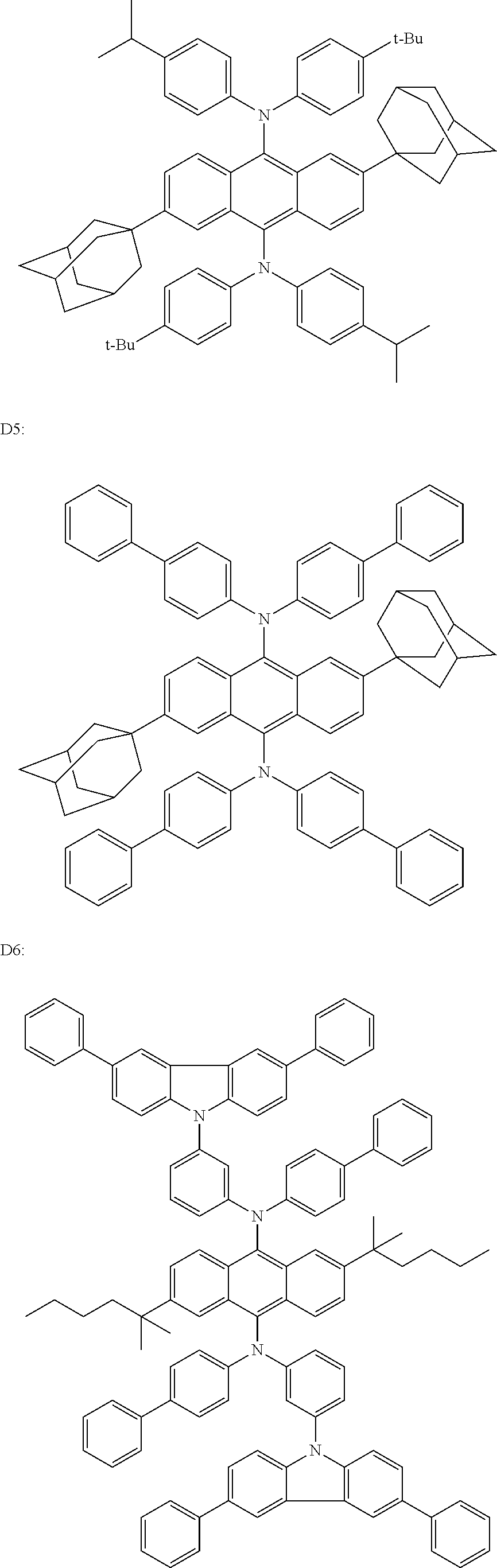


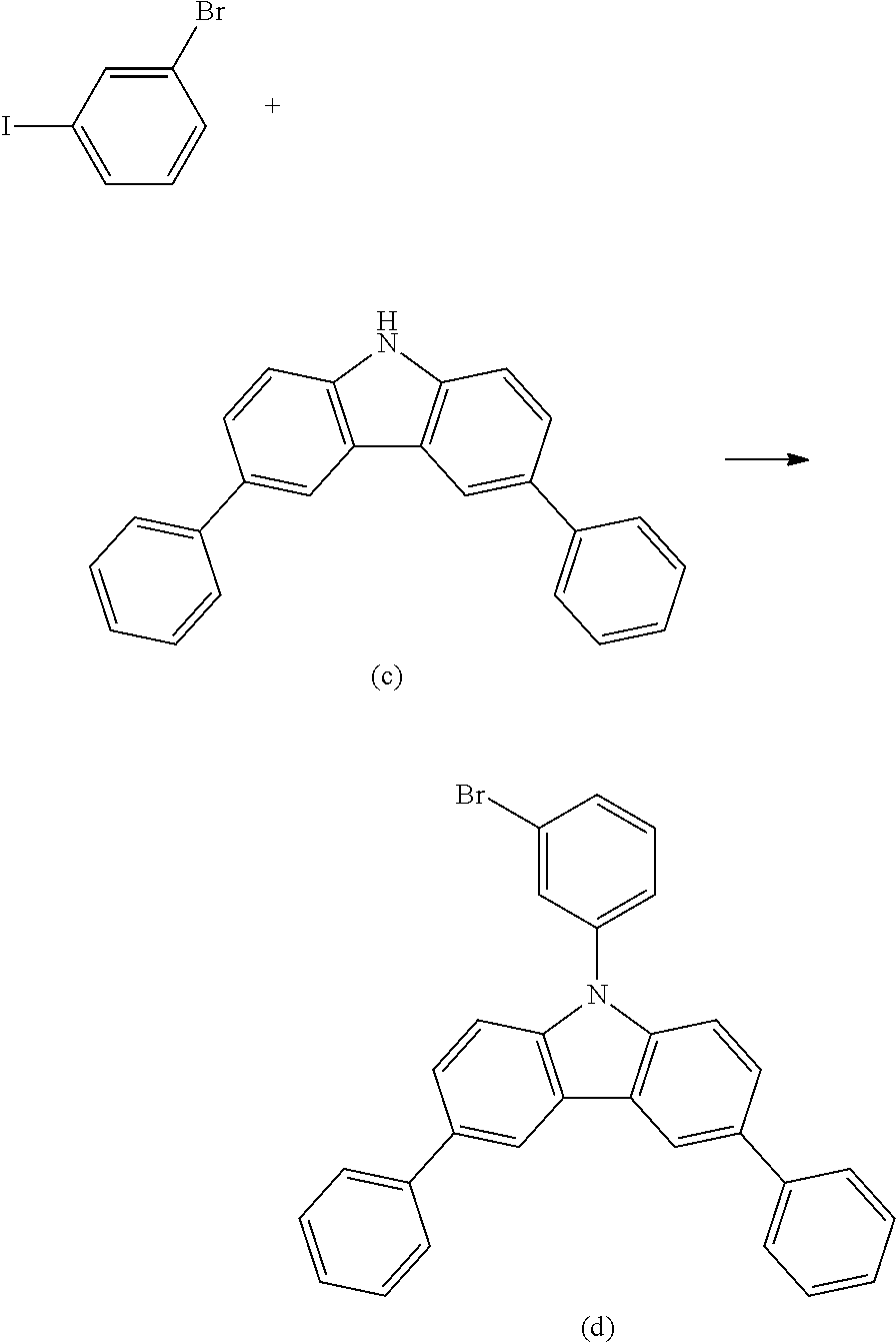


This compound can be prepared according to the following scheme:

Synthesis of Compound 2:


where “D/H” indicates approximately equal probability of H or D at this atomic position. The structure was confirmed by 1H NMR, 13H NMR, 2D NMR and 1H-13C HSQC (Heteronuclear Single Quantum Coherence).
-
- hole transport layer=polymer P1, which is a non-crosslinked arylamine polymer (20 nm)
- electroactive layer=13:1 host:dopant (40 nm), as shown in Table 1
- electron transport layer=ET1, which is a metal quinolate derivative (10 nm)
- cathode=CsF/Al (1.0/100 nm)
| TABLE 1 |
| Device Electroactive Layers |
| Example | Host | Dopant | ||
| Comparative B-1 | Comp. Compound A | D12 | ||
| Comparative B-2 | Comp. Compound A | D12 | ||
| Comparative B-3 | Comp. Compound A | D12 | ||
| Comparative B-4 | Comp. Compound A | D12 | ||
| Ex. 2-1 | H14 | D12 | ||
| Ex. 2-2 | H14 | D12 | ||
| Ex. 2-3 | H14 | D12 | ||
| Ex. 2-4 | H14 | D12 | ||
| Comparative C-1 | Comp. Compound A | D13 | ||
| Comparative C-2 | Comp. Compound A | D13 | ||
| Ex. 3-1 | H14 | D13 | ||
| Ex. 3-2 | H14 | D13 | ||
| TABLE 2 |
| Device Performance |
| Lifetest | |||||||||
| current | Lifetest | Raw | Projected | ||||||
| CIE | Voltage | C.E. | E.Q.E. | P.E. | density | Luminance | T50 | Lifetime T50 | |
| Ex. | (x, y) | (V) | (cd/A) | (%) | (lm/W) | (mA/cm2) | (nits) | (h) | @1000 nits |
| Comp. | 0.135, | 4.4 | 6.1 | 6.0 | 4.3 | 129 | 6837 | 410 | 10766 |
| B-1 | 0.124 | ||||||||
| Comp. | 0.135, | 4.3 | 6.4 | 6.1 | 4.7 | 125 | 7002 | 410 | 11211 |
| B-2 | 0.127 | ||||||||
| Comp. | 0.136, | 4.4 | 5.7 | 5.6 | 4.1 | 127 | 5906 | 430 | 8804 |
| B-3 | 0.123 | ||||||||
| Comp. | 0.134, | 4.3 | 6.4 | 6.1 | 4.7 | 123 | 7021 | 430 | 11813 |
| B-4 | 0.129 | ||||||||
| Ex. | 0.136, | 4.4 | 5.7 | 5.7 | 4.1 | 136 | 7040 | 870 | 24010 |
| 2-1 | 0.119 | ||||||||
| Ex. | 0.137, | 4.2 | 5.4 | 5.5 | 4.1 | 126 | 6244 | 830 | 18679 |
| 2-2 | 0.117 | ||||||||
| Ex. | 0.136, | 4.2 | 5.7 | 5.7 | 4.2 | 129 | 6467 | 830 | 19828 |
| 2-3 | 0.118 | ||||||||
| Ex. | 0.136, | 4.3 | 5.5 | 5.6 | 4.1 | 121 | 6148 | 870 | 19071 |
| 2-4 | 0.118 | ||||||||
| Comp. | 0.135, | 4.3 | 6.2 | 6.0 | 4.6 | 141 | 8018 | 490 | 16871 |
| C-1 | 0.128 | ||||||||
| Comp. | 0.135, | 4.3 | 6.3 | 6.0 | 4.6 | 125 | 7136 | 510 | 14403 |
| C-2 | 0.128 | ||||||||
| Ex. | 0.135, | 4.3 | 6.0 | 5.9 | 4.4 | 121 | 6741 | 950 | 24356 |
| 3-1 | 0.122 | ||||||||
| Ex. | 0.135, | 4.2 | 6 | 5.8 | 4.4 | 126 | 6974 | 930 | 25257 |
| 3-2 | 0.124 | ||||||||
| * All data @ 1000 nits, | |||||||||
| CE = current efficiency; | |||||||||
| CIEx and CIEy are the x and y color coordinates according to the C.I.E. chromaticity scale (Commission Internationale de L'Eclairage, 1931). | |||||||||
| Raw T50 is the time in hours for a device to reach one-half the initial luminance at the lifetest luminance given. | |||||||||
| Projected T50 is the projected lifetime at 1000 nits using an accelerator factor of 1.7. | |||||||||


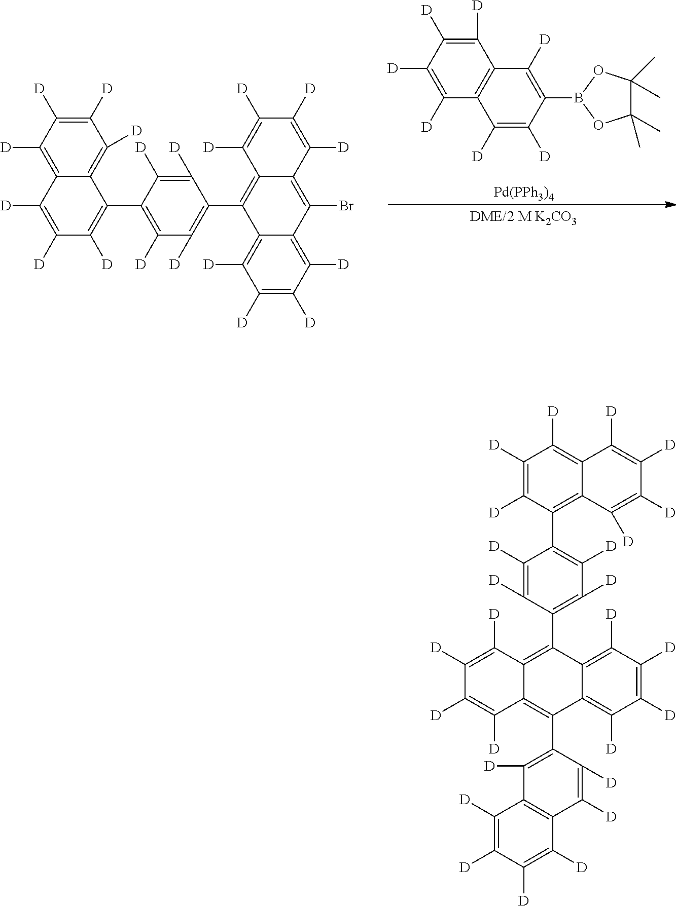


| TABLE 3 |
| Device Electroactive Layers |
| Example | Host | D13 | ||
| Comparative D-1 | Comp. Compound A | D13 | ||
| Comparative D-2 | Comp. Compound A | D13 | ||
| Ex. 8-1 | H11 | D13 | ||
| Ex. 8-2 | H11 | D13 | ||
| Ex. 9-1 | H8 | D13 | ||
| Ex. 9-2 | H8 | D13 | ||
| Comparative E-1 | Comp. Compound A | D13 | ||
| Comparative E-2 | Comp. Compound A | D13 | ||
| Ex. 10-1 | H10 | D13 | ||
| Ex. 10-2 | H10 | D13 | ||
| TABLE 4 |
| Device Performance |
| Lifetest | |||||||||
| current | Lifetest | Raw | Projected | ||||||
| CIE | Voltage | C.E. | E.Q.E. | P.E. | density | Luminance | T50 | Lifetime T50 | |
| Ex. | (x, y) | (V) | (cd/A) | (%) | (lm/W) | (mA/cm2) | (nits) | (h) | @1000 nits |
| Comp. | 0.136, | 4.4 | 5.7 | 5.5 | 4.1 | 127 | 6686 | 455 | 11503 |
| D-1 | 0.126 | ||||||||
| Comp. | 0.136, | 4.4 | 5.8 | 5.7 | 4.2 | 129 | 6572 | 450 | 11048 |
| D-2 | 0.123 | ||||||||
| Ex. | 0.136, | 4.4 | 5.8 | 5.8 | 4.2 | 128 | 6669 | 555 | 13970 |
| 8-1 | 0.121 | ||||||||
| Ex. | 0.136, | 4.3 | 5.9 | 5.7 | 4.2 | 130 | 6599 | 590 | 14587 |
| 8-2 | 0.124 | ||||||||
| Ex. | 0.136, | 4.3 | 5.8 | 5.8 | 4.2 | 127 | 6475 | 940 | 22503 |
| 9-1 | 0.121 | ||||||||
| Ex. | 0.136, | 4.4 | 5.8 | 5.8 | 4.2 | 124 | 6254 | 955 | 21551 |
| 9-2 | 0.121 | ||||||||
| Comp. | 0.136, | 4.4 | 6.1 | 6.0 | 4.3 | 124 | 6670 | 400 | 10071 |
| E-1 | 0.123 | ||||||||
| Comp. | 0.135, | 4.4 | 5.8 | 5.6 | 4.1 | 131 | 7006 | 388 | 10620 |
| E-2 | 0.124 | ||||||||
| Ex. | 0.136, | 4.4 | 6.0 | 5.9 | 4.2 | 123 | 6403 | 622 | 14610 |
| 10-1 | 0.121 | ||||||||
| Ex. | 0.136, | 4.4 | 5.7 | 5.8 | 4.1 | 121 | 6050 | 675 | 14398 |
| 10-2 | 0.118 | ||||||||
| * All data @ 1000 nits, | |||||||||
| CE = current efficiency; | |||||||||
| CIEx and CIEy are the x and y color coordinates according to the C.I.E. chromaticity scale (Commission Internationale de L'Eclairage, 1931). | |||||||||
| Raw T50 is the time in hours for a device to reach one-half the initial luminance at the lifetest luminance given. | |||||||||
| Projected T50 is the projected lifetime at 1000 nits using an accelerator factor of 1.7. | |||||||||
| TABLE 5 |
| Device lifetimes |
| Average Projected Lifetime T50 @ | |||
| Host | 1000 nits, in hours | ||
| Comparative Compound A | 11,276 and 10,346 | ||
| H8 | 22,027 | ||
| H10 | 14,504 | ||
| H11 | 14,279 | ||

-
- hole transport layer=polymer P1 (20 nm)
- electroactive layer=82.5:5:12.5 first host:second host:dopant (60 nm), as shown in Table 6
- electron transport layer=ET2 (10 nm).
- cathode=CsF/Al (0.7/100 nm)
| TABLE 6 |
| Device Electroactive Layers |
| Example | First Host | Second Host | Dopant | ||
| Comparative F | Comparative | D12 | D6 | ||
| Compound A | |||||
| Ex. 11 | H8 | D12 | D6 | ||
| TABLE 7 |
| Device Performance |
| Lifetest | |||||||||
| current | Lifetest | Raw | Projected | ||||||
| CIE | Voltage | C.E. | E.Q.E. | P.E. | density | Luminance | T50 | Lifetime T50 | |
| Ex. | (x, y) | (V) | (cd/A) | (%) | (lm/W) | (mA/cm2) | (nits) | (h) | @1000 nits |
| Comp. F | 0.265, | 4.8 | 26.1 | 7.2 | 17.1 | 134 | 29167 | 1800 | 557,000 |
| 0.649 | |||||||||
| Ex. 11 | 0.257, | 4.7 | 25.4 | 7.1 | 16.9 | 127 | 27232 | 4160 | 1,144,800 |
| 0.650 | |||||||||
| * All data @ 1000 nits, | |||||||||
| CE = current efficiency; | |||||||||
| CIEx and CIEy are the x and y color coordinates according to the C.I.E. chromaticity scale (Commission Internationale de L'Eclairage, 1931). | |||||||||
| Raw T50 is the time in hours for a device to reach one-half the initial luminance at the lifetest luminance given. | |||||||||
| Projected T50 is the projected lifetime at 1000 nits using an accelerator factor of 1.7. | |||||||||
Claims (28)


Priority Applications (3)
| Application Number | Priority Date | Filing Date | Title |
|---|---|---|---|
| US12/643,420 US8759818B2 (en) | 2009-02-27 | 2009-12-21 | Deuterated compounds for electronic applications |
| US13/786,769 US8890131B2 (en) | 2009-02-27 | 2013-03-06 | Deuterated compounds for electronic applications |
| US14/509,757 US9577199B2 (en) | 2009-02-27 | 2014-10-08 | Deuterated compounds for electronic applications |
Applications Claiming Priority (4)
| Application Number | Priority Date | Filing Date | Title |
|---|---|---|---|
| US15618109P | 2009-02-27 | 2009-02-27 | |
| US17940709P | 2009-05-19 | 2009-05-19 | |
| US23957409P | 2009-09-03 | 2009-09-03 | |
| US12/643,420 US8759818B2 (en) | 2009-02-27 | 2009-12-21 | Deuterated compounds for electronic applications |
Related Child Applications (1)
| Application Number | Title | Priority Date | Filing Date |
|---|---|---|---|
| US13/786,769 Continuation US8890131B2 (en) | 2009-02-27 | 2013-03-06 | Deuterated compounds for electronic applications |
Publications (2)
| Publication Number | Publication Date |
|---|---|
| US20110037057A1 US20110037057A1 (en) | 2011-02-17 |
| US8759818B2 true US8759818B2 (en) | 2014-06-24 |
Family
ID=43588061
Family Applications (3)
| Application Number | Title | Priority Date | Filing Date |
|---|---|---|---|
| US12/643,420 Active 2030-07-27 US8759818B2 (en) | 2009-02-27 | 2009-12-21 | Deuterated compounds for electronic applications |
| US13/786,769 Active 2030-01-02 US8890131B2 (en) | 2009-02-27 | 2013-03-06 | Deuterated compounds for electronic applications |
| US14/509,757 Active 2030-10-28 US9577199B2 (en) | 2009-02-27 | 2014-10-08 | Deuterated compounds for electronic applications |
Family Applications After (2)
| Application Number | Title | Priority Date | Filing Date |
|---|---|---|---|
| US13/786,769 Active 2030-01-02 US8890131B2 (en) | 2009-02-27 | 2013-03-06 | Deuterated compounds for electronic applications |
| US14/509,757 Active 2030-10-28 US9577199B2 (en) | 2009-02-27 | 2014-10-08 | Deuterated compounds for electronic applications |
Country Status (1)
| Country | Link |
|---|---|
| US (3) | US8759818B2 (en) |
Cited By (6)
| Publication number | Priority date | Publication date | Assignee | Title |
|---|---|---|---|---|
| KR20200047398A (en) | 2018-10-26 | 2020-05-07 | 롬엔드하스전자재료코리아유한회사 | Organic electroluminescent compound and organic electroluminescent device comprising the same |
| US20210384430A1 (en) * | 2018-10-03 | 2021-12-09 | Idemitsu Kosan Co.,Ltd. | Organic electroluminescence device and electronic apparatus provided with the same |
| DE102022112831A1 (en) | 2021-05-26 | 2022-12-01 | Rohm And Haas Electronic Materials Korea Ltd. | PROCESSES FOR THE PRODUCTION OF DEUTERED ORGANIC COMPOUNDS |
| US11581487B2 (en) | 2017-04-26 | 2023-02-14 | Oti Lumionics Inc. | Patterned conductive coating for surface of an opto-electronic device |
| US11730012B2 (en) | 2019-03-07 | 2023-08-15 | Oti Lumionics Inc. | Materials for forming a nucleation-inhibiting coating and devices incorporating same |
| US11751415B2 (en) | 2018-02-02 | 2023-09-05 | Oti Lumionics Inc. | Materials for forming a nucleation-inhibiting coating and devices incorporating same |
Families Citing this family (64)
| Publication number | Priority date | Publication date | Assignee | Title |
|---|---|---|---|---|
| KR101191644B1 (en) * | 2010-05-18 | 2012-10-17 | 삼성디스플레이 주식회사 | Organic material and organic light emitting device using the same |
| WO2012083301A1 (en) * | 2010-12-17 | 2012-06-21 | E. I. Du Pont De Nemours And Company | Anthracene derivative compounds for electronic applications |
| TW201245408A (en) * | 2011-04-08 | 2012-11-16 | Du Pont | Electronic device |
| US10586929B2 (en) * | 2013-12-12 | 2020-03-10 | Lg Chem, Ltd. | Solvent-resistant hole transport layers |
| US10297762B2 (en) | 2014-07-09 | 2019-05-21 | Universal Display Corporation | Organic electroluminescent materials and devices |
| US10749113B2 (en) | 2014-09-29 | 2020-08-18 | Universal Display Corporation | Organic electroluminescent materials and devices |
| US10361375B2 (en) | 2014-10-06 | 2019-07-23 | Universal Display Corporation | Organic electroluminescent materials and devices |
| US11522140B2 (en) | 2015-08-17 | 2022-12-06 | Universal Display Corporation | Organic electroluminescent materials and devices |
| US20180370999A1 (en) | 2017-06-23 | 2018-12-27 | Universal Display Corporation | Organic electroluminescent materials and devices |
| US11228010B2 (en) | 2017-07-26 | 2022-01-18 | Universal Display Corporation | Organic electroluminescent materials and devices |
| US11744142B2 (en) | 2017-08-10 | 2023-08-29 | Universal Display Corporation | Organic electroluminescent materials and devices |
| US20190161504A1 (en) | 2017-11-28 | 2019-05-30 | University Of Southern California | Carbene compounds and organic electroluminescent devices |
| US11937503B2 (en) | 2017-11-30 | 2024-03-19 | Universal Display Corporation | Organic electroluminescent materials and devices |
| US11542289B2 (en) | 2018-01-26 | 2023-01-03 | Universal Display Corporation | Organic electroluminescent materials and devices |
| KR102136806B1 (en) * | 2018-03-28 | 2020-07-23 | 엘지디스플레이 주식회사 | Novel organic compounds and an organic electroluminescent device comprising the same |
| KR102091507B1 (en) * | 2018-07-24 | 2020-03-20 | 머티어리얼사이언스 주식회사 | Organic electroluminescent device |
| US20200075870A1 (en) | 2018-08-22 | 2020-03-05 | Universal Display Corporation | Organic electroluminescent materials and devices |
| WO2020050217A1 (en) * | 2018-09-07 | 2020-03-12 | 出光興産株式会社 | Compound, material for organic electroluminescent element, organic electroluminescent element, and electronic device |
| US20230047477A1 (en) * | 2018-10-16 | 2023-02-16 | Idemitsu Kosan Co.,Ltd. | Organic electroluminescence device and electronic apparatus |
| US20230042023A1 (en) * | 2018-10-16 | 2023-02-09 | Idemitsu Kosan Co.,Ltd. | Organic electroluminescence device and electronic apparatus |
| WO2020111602A1 (en) | 2018-11-27 | 2020-06-04 | 주식회사 엘지화학 | Novel compound and organic light-emitting element including same |
| JP7172001B2 (en) * | 2018-11-27 | 2022-11-16 | エルジー・ケム・リミテッド | Novel compound and organic light-emitting device containing the same |
| US11737349B2 (en) | 2018-12-12 | 2023-08-22 | Universal Display Corporation | Organic electroluminescent materials and devices |
| KR20200081983A (en) * | 2018-12-28 | 2020-07-08 | 엘지디스플레이 주식회사 | Organic light emitting diode and orgnic light emitting device including the same |
| US11780829B2 (en) | 2019-01-30 | 2023-10-10 | The University Of Southern California | Organic electroluminescent materials and devices |
| US20200251664A1 (en) | 2019-02-01 | 2020-08-06 | Universal Display Corporation | Organic electroluminescent materials and devices |
| US11139442B2 (en) | 2019-03-12 | 2021-10-05 | Universal Display Corporation | Nanopatch antenna outcoupling structure for use in OLEDs |
| US11637261B2 (en) | 2019-03-12 | 2023-04-25 | Universal Display Corporation | Nanopatch antenna outcoupling structure for use in OLEDs |
| US11569480B2 (en) | 2019-03-12 | 2023-01-31 | Universal Display Corporation | Plasmonic OLEDs and vertical dipole emitters |
| JP2020158491A (en) | 2019-03-26 | 2020-10-01 | ユニバーサル ディスプレイ コーポレイション | Organic electroluminescent materials and devices |
| US20210032278A1 (en) | 2019-07-30 | 2021-02-04 | Universal Display Corporation | Organic electroluminescent materials and devices |
| US20210047354A1 (en) | 2019-08-16 | 2021-02-18 | Universal Display Corporation | Organic electroluminescent materials and devices |
| US20220359829A1 (en) * | 2019-09-13 | 2022-11-10 | Idemitsu Kosan Co.,Ltd. | Organic electroluminescent element and electronic device |
| US20210135130A1 (en) | 2019-11-04 | 2021-05-06 | Universal Display Corporation | Organic electroluminescent materials and devices |
| JP2021082801A (en) | 2019-11-14 | 2021-05-27 | ユニバーサル ディスプレイ コーポレイション | Organic electroluminescence material and device |
| US20210217969A1 (en) | 2020-01-06 | 2021-07-15 | Universal Display Corporation | Organic electroluminescent materials and devices |
| US20220336759A1 (en) | 2020-01-28 | 2022-10-20 | Universal Display Corporation | Organic electroluminescent materials and devices |
| EP3937268A1 (en) | 2020-07-10 | 2022-01-12 | Universal Display Corporation | Plasmonic oleds and vertical dipole emitters |
| US20220112232A1 (en) | 2020-10-02 | 2022-04-14 | Universal Display Corporation | Organic electroluminescent materials and devices |
| US20220158096A1 (en) | 2020-11-16 | 2022-05-19 | Universal Display Corporation | Organic electroluminescent materials and devices |
| US20220165967A1 (en) | 2020-11-24 | 2022-05-26 | Universal Display Corporation | Organic electroluminescent materials and devices |
| US20220162243A1 (en) | 2020-11-24 | 2022-05-26 | Universal Display Corporation | Organic electroluminescent materials and devices |
| US20220271241A1 (en) | 2021-02-03 | 2022-08-25 | Universal Display Corporation | Organic electroluminescent materials and devices |
| EP4059915A3 (en) | 2021-02-26 | 2022-12-28 | Universal Display Corporation | Organic electroluminescent materials and devices |
| EP4060758A3 (en) | 2021-02-26 | 2023-03-29 | Universal Display Corporation | Organic electroluminescent materials and devices |
| US20220298192A1 (en) | 2021-03-05 | 2022-09-22 | Universal Display Corporation | Organic electroluminescent materials and devices |
| US20220298190A1 (en) | 2021-03-12 | 2022-09-22 | Universal Display Corporation | Organic electroluminescent materials and devices |
| US20220298193A1 (en) | 2021-03-15 | 2022-09-22 | Universal Display Corporation | Organic electroluminescent materials and devices |
| US20220340607A1 (en) | 2021-04-05 | 2022-10-27 | Universal Display Corporation | Organic electroluminescent materials and devices |
| EP4075531A1 (en) | 2021-04-13 | 2022-10-19 | Universal Display Corporation | Plasmonic oleds and vertical dipole emitters |
| US20220352478A1 (en) | 2021-04-14 | 2022-11-03 | Universal Display Corporation | Organic eletroluminescent materials and devices |
| US20230006149A1 (en) | 2021-04-23 | 2023-01-05 | Universal Display Corporation | Organic electroluminescent materials and devices |
| US20220407020A1 (en) | 2021-04-23 | 2022-12-22 | Universal Display Corporation | Organic electroluminescent materials and devices |
| US20230133787A1 (en) | 2021-06-08 | 2023-05-04 | University Of Southern California | Molecular Alignment of Homoleptic Iridium Phosphors |
| EP4151699A1 (en) | 2021-09-17 | 2023-03-22 | Universal Display Corporation | Organic electroluminescent materials and devices |
| EP4212539A1 (en) | 2021-12-16 | 2023-07-19 | Universal Display Corporation | Organic electroluminescent materials and devices |
| EP4231804A3 (en) | 2022-02-16 | 2023-09-20 | Universal Display Corporation | Organic electroluminescent materials and devices |
| US20230292605A1 (en) | 2022-03-09 | 2023-09-14 | Universal Display Corporation | Organic electroluminescent materials and devices |
| US20230292592A1 (en) | 2022-03-09 | 2023-09-14 | Universal Display Corporation | Organic electroluminescent materials and devices |
| US20230337516A1 (en) | 2022-04-18 | 2023-10-19 | Universal Display Corporation | Organic electroluminescent materials and devices |
| US20230389421A1 (en) | 2022-05-24 | 2023-11-30 | Universal Display Corporation | Organic electroluminescent materials and devices |
| EP4293001A1 (en) | 2022-06-08 | 2023-12-20 | Universal Display Corporation | Organic electroluminescent materials and devices |
| US20240016051A1 (en) | 2022-06-28 | 2024-01-11 | Universal Display Corporation | Organic electroluminescent materials and devices |
| US20240107880A1 (en) | 2022-08-17 | 2024-03-28 | Universal Display Corporation | Organic electroluminescent materials and devices |
Citations (245)
| Publication number | Priority date | Publication date | Assignee | Title |
|---|---|---|---|---|
| US3282875A (en) | 1964-07-22 | 1966-11-01 | Du Pont | Fluorocarbon vinyl ether polymers |
| US3849458A (en) | 1966-01-21 | 1974-11-19 | Incentive Res & Dev Ab | Method for deuterating organic compounds |
| US4053311A (en) | 1976-04-02 | 1977-10-11 | Limburg William W | Poly-n-vinylcarbazole image transport layer plasticized by bis(4-diethylamino-2-methylphenyl)phenylmethane |
| US4358545A (en) | 1980-06-11 | 1982-11-09 | The Dow Chemical Company | Sulfonic acid electrolytic cell having flourinated polymer membrane with hydration product less than 22,000 |
| US4940525A (en) | 1987-05-08 | 1990-07-10 | The Dow Chemical Company | Low equivalent weight sulfonic fluoropolymers |
| US5247190A (en) | 1989-04-20 | 1993-09-21 | Cambridge Research And Innovation Limited | Electroluminescent devices |
| US5254633A (en) | 1991-07-10 | 1993-10-19 | Allied Signal Inc. | Process for the preparation of conductive polymer blends |
| US5378519A (en) | 1992-04-28 | 1995-01-03 | Canon Kabushiki Kaisha | Electroluminescent device |
| US5408109A (en) | 1991-02-27 | 1995-04-18 | The Regents Of The University Of California | Visible light emitting diodes fabricated from soluble semiconducting polymers |
| EP0443861B1 (en) | 1990-02-23 | 1995-07-05 | Sumitomo Chemical Company Limited | Organic electroluminescence device |
| US5707747A (en) | 1993-11-01 | 1998-01-13 | Hodogaya Chemical Co., Ltd. | Amine compound and electro-luminescence device comprising same |
| US5911918A (en) | 1992-06-03 | 1999-06-15 | Monsanto Company | Surface dopants as blend compatibilizers in conjugated polymers |
| US5929194A (en) | 1996-02-23 | 1999-07-27 | The Dow Chemical Company | Crosslinkable or chain extendable polyarylpolyamines and films thereof |
| US5936259A (en) | 1997-10-16 | 1999-08-10 | Lucent Technologies Inc. | Thin film transistor and organic semiconductor material thereof |
| US5962631A (en) | 1995-07-28 | 1999-10-05 | The Dow Chemical Company | 2, 7-aryl-9-substituted fluorenes and 9-substituted fluorene oligomers and polymers |
| WO1999054385A1 (en) | 1998-04-21 | 1999-10-28 | The Dow Chemical Company | Fluorene-containing polymers and electroluminescent devices therefrom |
| JP2000068073A (en) | 1998-08-27 | 2000-03-03 | Futaba Corp | Organic electroluminescent element and its manufacture |
| JP2000186066A (en) | 1998-12-22 | 2000-07-04 | Minolta Co Ltd | New amino compound, its production and use thereof |
| WO2000053565A1 (en) | 1999-03-11 | 2000-09-14 | Mobil Oil Corporation | Process for preparing organic carbonates |
| US6150426A (en) | 1996-10-15 | 2000-11-21 | E. I. Du Pont De Nemours And Company | Compositions containing particles of highly fluorinated ion exchange polymer |
| WO2000070655A2 (en) | 1999-05-13 | 2000-11-23 | The Trustees Of Princeton University | Very high efficiency organic light emitting devices based on electrophosphorescence |
| EP1061112A1 (en) | 1998-12-28 | 2000-12-20 | Idemitsu Kosan Company Limited | Organic electroluminescent element |
| JP2001039933A (en) | 1999-07-30 | 2001-02-13 | Mitsui Chemicals Inc | Amine compound |
| WO2001041512A1 (en) | 1999-12-01 | 2001-06-07 | The Trustees Of Princeton University | Complexes of form l2mx as phosphorescent dopants for organic leds |
| US6259202B1 (en) | 1996-06-12 | 2001-07-10 | The Trustees Of Princeton University | Plasma treatment of conductive layers |
| JP2001226331A (en) | 2000-02-14 | 2001-08-21 | Mitsui Chemicals Inc | Amine compound and organic electroluminescent element containing the compound |
| US6303238B1 (en) | 1997-12-01 | 2001-10-16 | The Trustees Of Princeton University | OLEDs doped with phosphorescent compounds |
| US20010053462A1 (en) | 2000-05-02 | 2001-12-20 | Masayuki Mishima | Light-emitting device |
| US20020048687A1 (en) | 2000-03-29 | 2002-04-25 | Idemitsu Kosan Co., Ltd. | Anthracene derivative and organic electroluminescence device using the derivative |
| US20020076576A1 (en) | 2000-12-07 | 2002-06-20 | Li Xiao-Chang Charles | Deuterated semiconducting organic compounds used for opto-electronic devices |
| WO2002051958A1 (en) | 2000-12-23 | 2002-07-04 | Johnson Matthey Public Limited Company | Electroactive polyarylamine-type compositions |
| US20020155319A1 (en) | 1999-02-15 | 2002-10-24 | Idemitsu Kosan Co., Ltd. | Organic electroluminescent device and method of manufacture thereof |
| EP1277824A1 (en) | 2001-07-19 | 2003-01-22 | Sumitomo Chemical Company, Limited | Polymeric fluorescent substance and polymer light-emitting device using the same |
| JP2003026641A (en) | 2001-07-13 | 2003-01-29 | Mitsubishi Chemicals Corp | Binaphthyl compound, method for producing the same and organic electroluminescent element |
| WO2003008424A1 (en) | 2001-07-18 | 2003-01-30 | E.I. Du Pont De Nemours And Company | Luminescent lanthanide complexes with imine ligands and devices made with such complexes |
| CN1416301A (en) | 2001-10-30 | 2003-05-07 | Lg电子株式会社 | Organic electroluminescent element |
| WO2003040257A1 (en) | 2001-11-07 | 2003-05-15 | E. I. Du Pont De Nemours And Company | Electroluminescent platinum compounds and devices made with such compounds |
| WO2003063555A1 (en) | 2001-12-26 | 2003-07-31 | E. I. Du Pont De Nemours And Company | Electroluminescent iridium compounds wiht fluorinated phenylpyridines, phenylpyrimidines, and phenylquinolines and devices made with such compounds |
| JP2003238501A (en) | 2002-02-18 | 2003-08-27 | Idemitsu Kosan Co Ltd | Aromatic oligoamine derivative and organic electroluminescent element containing the same |
| US20030168970A1 (en) | 2000-11-24 | 2003-09-11 | Tsuyoshi Tominaga | Luminescent element material and luminescent element comprising the same |
| JP2003297582A (en) | 2002-01-31 | 2003-10-17 | Sumitomo Chem Co Ltd | Organic electroluminescent element |
| WO2003091688A2 (en) | 2001-07-05 | 2003-11-06 | E.I. Du Pont De Nemours And Company | Photoactive lanthanide complexes with phosphine oxides, phosphine oxide-sulfides, pyridine n-oxides, and phosphine oxide-pyridine n-oxides, and devices made with such complexes |
| JP2003338380A (en) | 2002-05-21 | 2003-11-28 | Toshiba Corp | Ink for organic el hole injection layer, manufacturing method therefor, manufacturing method for organic el display device, and organic el display device |
| US20030224205A1 (en) | 2002-04-19 | 2003-12-04 | 3M Innovative Properties Company | Electroluminescent materials and methods of manufacture and use |
| US20030227001A1 (en) | 2002-06-04 | 2003-12-11 | Canon Kabushiki Kaisha | Organic photoluminescent polymers with improved stability |
| US6670645B2 (en) | 2000-06-30 | 2003-12-30 | E. I. Du Pont De Nemours And Company | Electroluminescent iridium compounds with fluorinated phenylpyridines, phenylpyrimidines, and phenylquinolines and devices made with such compounds |
| US20040004433A1 (en) | 2002-06-26 | 2004-01-08 | 3M Innovative Properties Company | Buffer layers for organic electroluminescent devices and methods of manufacture and use |
| JP2004010550A (en) * | 2002-06-07 | 2004-01-15 | Japan Science & Technology Corp | Method for producing deuterated aromatic compound |
| JP2004014187A (en) | 2002-06-04 | 2004-01-15 | Mitsubishi Chemicals Corp | Organic electroluminescent element |
| WO2004016710A1 (en) | 2002-08-15 | 2004-02-26 | E.I. Du Pont De Nemours And Company | Compounds comprising phosphorus-containing metal complexes |
| US20040038459A1 (en) | 2000-11-28 | 2004-02-26 | Brown Beverley Anne | Field effect transistors and materials and methods for their manufacture |
| JP2004071286A (en) | 2002-08-05 | 2004-03-04 | Dainippon Printing Co Ltd | Manufacturing method of electroluminescent element |
| WO2004018587A1 (en) | 2002-08-23 | 2004-03-04 | Idemitsu Kosan Co., Ltd. | Organic electroluminescence device and anthracene derivative |
| JP2004107292A (en) | 2002-09-20 | 2004-04-08 | Tosoh Corp | New binaphthalene derivative and method for producing the same |
| US20040082250A1 (en) | 2002-03-25 | 2004-04-29 | Dai Nippon Printing Co Ltd | Process for producing electrode for electroluminescence |
| US20040094768A1 (en) | 2002-09-06 | 2004-05-20 | Gang Yu | Methods for producing full-color organic electroluminescent devices |
| WO2004041901A1 (en) | 2002-11-08 | 2004-05-21 | Covion Organic Semiconductors Gmbh | Aryl-substituted polyindenofluorenes for use in organic electroluminiscent devices |
| US20040102577A1 (en) | 2002-09-24 | 2004-05-27 | Che-Hsiung Hsu | Water dispersible polythiophenes made with polymeric acid colloids |
| US20040106003A1 (en) | 2002-12-03 | 2004-06-03 | Canon Kabushiki Kaisha | Binaphthalene derivatives for organic electro-luminescent devices |
| US20040106004A1 (en) | 2002-12-03 | 2004-06-03 | Canon Kabushiki Kaisha | Organic light-emitting device based on spiro-type conjugated compounds |
| US20040121184A1 (en) | 2002-08-16 | 2004-06-24 | Thompson Mark E. | Organic light emitting materials and devices |
| US20040127637A1 (en) | 2002-09-24 | 2004-07-01 | Che-Hsiung Hsu | Water dispersible polyanilines made with polymeric acid colloids for electronics applications |
| EP1437395A2 (en) | 2002-12-24 | 2004-07-14 | Lg Electronics Inc. | Organic electroluminescent device |
| WO2004058913A1 (en) | 2002-12-24 | 2004-07-15 | Elam-T Limited | Electroluminescent materials and devices |
| JP2004224766A (en) | 2003-01-27 | 2004-08-12 | Idemitsu Kosan Co Ltd | Bisanthracene derivative, material for forming luminescent coating film and organic electroluminescent element |
| US20040209118A1 (en) | 2003-03-05 | 2004-10-21 | Lg Electronics Inc. | Organic electroluminescent device |
| EP1491609A2 (en) | 2003-06-27 | 2004-12-29 | Canon Kabushiki Kaisha | Substituted anthryl derivative and electroluminescence device using the same |
| EP1491610A2 (en) | 2003-06-27 | 2004-12-29 | Canon Kabushiki Kaisha | Organic electroluminescent device |
| US20040263067A1 (en) | 2003-06-27 | 2004-12-30 | Canon Kabushiki Kaisha | Anthryl derivative group substituted compound, and organic luminescent device making use of same |
| WO2005000787A1 (en) | 2003-06-27 | 2005-01-06 | Canon Kabushiki Kaisha | Aminoanthryl derivative substitution compound and organic electroluminescence device using the same |
| US6852429B1 (en) | 2003-08-06 | 2005-02-08 | Canon Kabushiki Kaisha | Organic electroluminescent device based on pyrene derivatives |
| US20050035335A1 (en) | 2000-01-18 | 2005-02-17 | Chien-Chung Han | Thermally stable self-doped functionalized polyanilines |
| US20050064233A1 (en) | 2002-07-19 | 2005-03-24 | Idemitsu Kosan Co., Ltd. | Organic electroluminescence device and organic light emitting medium |
| US20050063638A1 (en) | 2003-09-24 | 2005-03-24 | Alger William O. | Optical fibers embedded in a printed circuit board |
| US6875524B2 (en) | 2003-08-20 | 2005-04-05 | Eastman Kodak Company | White light-emitting device with improved doping |
| US20050074630A1 (en) | 2003-03-27 | 2005-04-07 | Hiroshi Kanno | Organic electroluminescent device |
| WO2005031889A2 (en) | 2003-09-24 | 2005-04-07 | E.I. Dupont De Nemours And Company | Method for the application of active materials onto active surfaces and devices made with such methods |
| US20050073249A1 (en) | 2003-08-19 | 2005-04-07 | Seiko Epson Corporation | Organic light-emitting device, manufacturing method thereof, and electronic apparatus thereof |
| US20050106415A1 (en) | 2003-10-22 | 2005-05-19 | Eastman Kodak Company | Aggregate organic light emitting diode devices with improved operational stability |
| WO2005049546A1 (en) | 2003-11-14 | 2005-06-02 | Sumitomo Chemical Company, Limited | Halogenated bisdiarylaminopolycylic aromatic compounds and polymers thereof |
| WO2005049548A1 (en) | 2003-11-17 | 2005-06-02 | Sumitomo Chemical Company, Limited | Crosslinkable substituted fluorene compounds |
| US6902833B2 (en) | 2003-04-01 | 2005-06-07 | University Of Southern California | Materials and structures for enhancing the performance or organic light emitting devices |
| WO2005052027A1 (en) | 2003-11-17 | 2005-06-09 | Sumitomo Chemical Company, Limited | Crosslinkable arylamine compounds and conjugated oligomers of polymers based thereon |
| US20050158577A1 (en) | 2002-06-26 | 2005-07-21 | Tadashi Ishibashi | Organic electroluminescent element and lumiscent device or display including the same |
| WO2005071773A1 (en) | 2004-01-08 | 2005-08-04 | Eastman Kodak Company | Stable organic light-emitting devices using aminoanthracenes |
| EP1561794A1 (en) | 2002-11-12 | 2005-08-10 | Idemitsu Kosan Co., Ltd. | Material for organic electroluminescent device and organic electroluminescent device using same |
| US20050187411A1 (en) | 2004-02-19 | 2005-08-25 | Norman Herron | Compositions comprising novel compounds and electronic devices made with such compositions |
| US20050184287A1 (en) | 2004-02-20 | 2005-08-25 | Norman Herron | Cross-linkable polymers and electronic devices made with such polymers |
| US20050186106A1 (en) | 2004-02-24 | 2005-08-25 | Sanyo Electric Co., Ltd. | Organic electroluminescent device and process for preparing the same |
| JP2005232452A (en) | 2004-02-10 | 2005-09-02 | Hc Starck Gmbh | Polythiophene composition for improving organic light emitting diode |
| US20050205860A1 (en) | 2004-03-17 | 2005-09-22 | Che-Hsiung Hsu | Water dispersible polypyrroles made with polymeric acid colloids for electronics applications |
| US6953705B2 (en) | 2003-07-22 | 2005-10-11 | E. I. Du Pont De Nemours And Company | Process for removing an organic layer during fabrication of an organic electronic device |
| US20050245752A1 (en) | 2004-04-29 | 2005-11-03 | Eastman Kodak Company | Synthesis of unsymmetric anthracene compounds |
| US20050244670A1 (en) | 2002-08-28 | 2005-11-03 | Canon Kabushiki Kaisha | Monoamino compound and organic luminescence device using the same |
| WO2005115950A1 (en) | 2004-05-27 | 2005-12-08 | Idemitsu Kosan Co., Ltd. | Asymmetric pyrene derivative and organic electroluminescent device using same |
| EP1604974A1 (en) | 2003-03-20 | 2005-12-14 | Idemitsu Kosan Co., Ltd. | Aromatic amine derivative and organic electroluminescent element made with the same |
| US20050280008A1 (en) * | 2004-06-16 | 2005-12-22 | Eastman Kodak Company | Array of light-emitting oled microcavity pixels |
| EP1612202A1 (en) | 2003-04-10 | 2006-01-04 | Idemitsu Kosan Co., Ltd. | Aromatic amine derivative and organic electroluminescent element employing the same |
| WO2006001333A1 (en) | 2004-06-28 | 2006-01-05 | Idemitsu Kosan Co., Ltd. | Polycyclic aromatic compound, material for forming luminescent coating film and organic electroluminescent device using same |
| JP2006016384A (en) | 2004-06-03 | 2006-01-19 | Mitsui Chemicals Inc | Amine compound, and organic electroluminescent device containing the same |
| EP1624500A1 (en) | 2004-08-05 | 2006-02-08 | Novaled GmbH | Spiro bifluorene compounds as organic semiconductor matrix materials |
| JP2006052323A (en) | 2004-08-12 | 2006-02-23 | Sony Corp | Organic material, organic electroluminescent element, and display device |
| WO2006025273A1 (en) | 2004-08-31 | 2006-03-09 | Idemitsu Kosan Co., Ltd. | Aromatic amine derivative and organic electroluminescent device using same |
| US20060076557A1 (en) | 2004-10-13 | 2006-04-13 | Waller Francis J | Aqueous dispersions of polythienothiophenes with fluorinated ion exchange polymers as dopants |
| WO2006043087A1 (en) | 2004-10-22 | 2006-04-27 | Cambridge Display Technology Limited | Monomer for making a crosslinked polymer |
| US20060099447A1 (en) | 2004-11-05 | 2006-05-11 | Samsung Sdi Co., Ltd. | Organic light-emitting device |
| US20060103298A1 (en) | 2004-11-17 | 2006-05-18 | Jun-Yeob Lee | Small molecular organic electroluminescent display device and method of fabricating the same |
| US20060115678A1 (en) | 2004-11-26 | 2006-06-01 | Canon Kabushiki Kaisha | Aminoanthryl derivative-substituted pyrene compound and organic light-emitting device |
| US20060115676A1 (en) | 2004-11-29 | 2006-06-01 | Canon Kabushiki Kaisha | Phenanthroline compound and light-emitting device |
| US20060113528A1 (en) | 2004-11-26 | 2006-06-01 | Canon Kabushiki Kaisha | Organic light-emitting device |
| WO2006057326A1 (en) | 2004-11-25 | 2006-06-01 | Pioneer Corporation | Pyrene compound and light emitting transistor device utilizing the same |
| US20060121312A1 (en) | 2004-11-26 | 2006-06-08 | Canon Kabushiki Kaisha | Fluorene compound and organic light-emitting device |
| US20060128969A1 (en) | 2004-12-14 | 2006-06-15 | Xerox Corporation | Process to form compound with indolocarbazole moieties |
| US20060127698A1 (en) | 2004-05-27 | 2006-06-15 | Idemitsu Kosan Co., Ltd. | White organic electroluminescent device |
| JP2006151844A (en) | 2004-11-26 | 2006-06-15 | Canon Inc | Aminoanthryl-derived-group-substituted compound and organic luminescent element |
| EP1672713A1 (en) | 2004-12-14 | 2006-06-21 | Xerox Corporation | Compound with indolocarbazole moieties and electronic devices containing such compound |
| US20060134459A1 (en) | 2004-12-17 | 2006-06-22 | Shouquan Huo | OLEDs with mixed-ligand cyclometallated complexes |
| WO2006063852A1 (en) | 2004-12-18 | 2006-06-22 | Merck Patent Gmbh | Electroluminescent polymers and use thereof |
| US7075102B2 (en) | 2000-06-30 | 2006-07-11 | E.I. Du Pont De Nemours And Company | Electroluminescent iridium compounds with fluorinated phenylpyridines, phenylpyrimidines, and phenylquinolines and devices made with such compounds |
| US20060159838A1 (en) | 2005-01-14 | 2006-07-20 | Cabot Corporation | Controlling ink migration during the formation of printable electronic features |
| US20060158102A1 (en) | 2004-12-01 | 2006-07-20 | Idemitsu Kosan Co., Ltd. | Organic electroluminescent device |
| WO2006076146A2 (en) | 2005-01-10 | 2006-07-20 | Polaroid Corporation | Method and apparatus for controlling the uniformity of print density of a thermal print head array |
| WO2006082705A1 (en) | 2005-02-07 | 2006-08-10 | Idemitsu Kosan Co., Ltd. | Aromatic amine derivative and organic electroluminescent device using same |
| WO2006085434A1 (en) | 2005-02-10 | 2006-08-17 | Idemitsu Kosan Co., Ltd. | Bisanthracene derivative and organic electroluminescent device using same |
| WO2006086040A2 (en) | 2004-11-24 | 2006-08-17 | The Trustees Of Princeton University | Organic photosensitive optoelectronic device having a phenanthroline exciton blocking layer |
| JP2006219392A (en) | 2005-02-09 | 2006-08-24 | Canon Inc | Bisanthryl derived group-substituted compound and organic light emitting device |
| WO2006090772A1 (en) | 2005-02-25 | 2006-08-31 | Toray Industries, Inc. | Material for light-emitting element and light emitting element |
| US20060210830A1 (en) | 2005-03-15 | 2006-09-21 | Idemitsu Kosan Co., Ltd. | Aromatic amine derivative and organic electroluminescence device using the same |
| US20060216411A1 (en) | 2003-09-17 | 2006-09-28 | Toppan Printing Co., Ltd | Electroluminescent device |
| US20060217572A1 (en) | 2005-03-25 | 2006-09-28 | Idemitsu Kosan Co., Ltd. | Aromatic amine derivative and organic electroluminescence device employing the same |
| US7125952B2 (en) | 2001-02-21 | 2006-10-24 | Cambridge Display Technology, Limited | (Partially) conjugated polymer process for its preparation and use in electroluminescent devices |
| WO2006112582A1 (en) | 2005-04-21 | 2006-10-26 | Doosan Corporation | Deuterated organic electroluminescent material, preparation method thereof and organic light emitting diode using the same |
| EP1718124A1 (en) | 2004-02-19 | 2006-11-02 | Idemitsu Kosan Co., Ltd. | White color organic electroluminescence device |
| US20060251925A1 (en) | 2005-04-18 | 2006-11-09 | Idemitsu Kosan Co., Ltd. | Aromatic amine derivative and organic electroluminescence device using the same |
| WO2006121237A1 (en) | 2005-05-07 | 2006-11-16 | Doosan Corporation | Novel deuterated aryl amine compound, preparation method thereof, and organic light emitting diode using the same |
| JP2006328037A (en) | 2005-04-25 | 2006-12-07 | Chemiprokasei Kaisha Ltd | Binaphthyl derivative, host material and hole transport material each made therefrom, and organic el device using the hole transport material |
| US20060284140A1 (en) | 2003-06-26 | 2006-12-21 | Esther Breuning | Novel materials for electroluminescence |
| EP1737277A1 (en) | 2004-04-15 | 2006-12-27 | Idemitsu Kosan Co., Ltd. | Organic electroluminescent device |
| WO2006137210A1 (en) | 2005-06-24 | 2006-12-28 | Idemitsu Kosan Co., Ltd. | Benzothiophene derivative and organic electroluminescence device making use of the same |
| WO2007004364A1 (en) | 2005-07-06 | 2007-01-11 | Idemitsu Kosan Co., Ltd. | Pyrene derivative and organic electroluminescence device making use of the same |
| US20070032632A1 (en) | 2003-08-14 | 2007-02-08 | Sony Chemicals Corp. | Electroluminescence polymer, organic el device, and display |
| US20070031701A1 (en) | 2005-08-04 | 2007-02-08 | Semiconductor Energy Laboratory Co., Ltd. | Carbazole derivative, light-emitting element material obtained by using carbazole derivative, light-emitting element, and electronic device |
| US20070031588A1 (en) | 2003-02-20 | 2007-02-08 | Fuji Photo Film Co., Ltd. | Organic EL device and its manufacture method |
| WO2007021117A1 (en) * | 2005-08-16 | 2007-02-22 | Gracel Display Inc. | Green electroluminescent compounds and organic electroluminescent device using the same |
| US7189989B2 (en) | 2002-08-22 | 2007-03-13 | Fuji Photo Film Co., Ltd. | Light emitting element |
| US20070066755A1 (en) | 2005-06-27 | 2007-03-22 | Che-Hsiung Hsu | Electrically conductive polymer compositions |
| WO2007046658A1 (en) | 2005-10-21 | 2007-04-26 | Lg Chem. Ltd. | New binaphthalene derivatives, preparation method thereof and organic electronic device using the same |
| US7211202B2 (en) | 2002-12-13 | 2007-05-01 | Atofina | Process to make a conductive composition of a fluorinated polymer which contains polyaniline |
| US20070099024A1 (en) | 2003-09-24 | 2007-05-03 | Kazumi Nii | Electrolumiscent device |
| WO2007054345A1 (en) | 2005-11-10 | 2007-05-18 | Novaled Ag | Doped organic semiconductor material |
| US20070114917A1 (en) | 2005-11-21 | 2007-05-24 | Idemitsu Kosan Co., Ltd. | Aromatic amine derivative and organic electroluminescence device employing the same |
| DE102005058557A1 (en) | 2005-12-08 | 2007-06-14 | Merck Patent Gmbh | Organic electroluminescent device |
| US20070134511A1 (en) | 2004-12-08 | 2007-06-14 | Idemitsu Kosan Co., Ltd. | Organic electroluminescence device |
| WO2007076146A2 (en) | 2005-12-27 | 2007-07-05 | E. I. Du Pont De Nemours And Company | Compositions comprising novel copolymers and electronic devices made with such compositions |
| JP2007182432A (en) | 2005-12-08 | 2007-07-19 | Mitsubishi Chemicals Corp | Organic compound, electric charge-transporting material, electric charge-transporting material composition and organic electric field light-emitting element |
| JP2007186449A (en) | 2006-01-13 | 2007-07-26 | Canon Inc | Compound substituted with aminobisanthryl-derived group and organic light-emitting element by using the same |
| WO2007086695A1 (en) | 2006-01-27 | 2007-08-02 | Lg Chem. Ltd. | New anthracene derivatives, preparation method thereof and organic light emitting diode using the same |
| US20070181874A1 (en) | 2004-12-30 | 2007-08-09 | Shiva Prakash | Charge transport layers and organic electron devices comprising same |
| US20070182321A1 (en) | 2006-02-09 | 2007-08-09 | Fujifilm Corporation | Organic electroluminescence device and producing method therefor |
| US20070189190A1 (en) | 2006-02-15 | 2007-08-16 | Feng Fujen | Topology discovery of a private network |
| JP2007208165A (en) | 2006-02-06 | 2007-08-16 | Toray Ind Inc | Light emitting element |
| US20070205409A1 (en) | 2006-03-02 | 2007-09-06 | Daniel David Lecloux | Process for making contained layers and devices made with same |
| WO2007100096A1 (en) | 2006-03-03 | 2007-09-07 | Idemitsu Kosan Co., Ltd. | Aromatic amine derivative and organic electroluminescent device using same |
| WO2007105917A1 (en) | 2006-03-15 | 2007-09-20 | Lg Chem, Ltd. | Novel anthracene derivatives, process for preparation thereof, and organic electronic light emitting device using the same |
| US20070215864A1 (en) | 2006-03-17 | 2007-09-20 | Luebben Silvia D | Use of pi-conjugated organoboron polymers in thin-film organic polymer electronic devices |
| WO2007108666A1 (en) | 2006-03-23 | 2007-09-27 | Lg Chem, Ltd. | New diamine derivatives, preparation method thereof and organic electronic device using the same |
| WO2007108457A1 (en) | 2006-03-20 | 2007-09-27 | Pioneer Corporation | Pyrene organic compound, transistor material and light emitting transistor element |
| KR100765728B1 (en) | 2006-03-31 | 2007-10-11 | 성균관대학교산학협력단 | Surface treatment method of ito using oxygen plasma and thermal treatment and oled device using the same method |
| WO2007116828A1 (en) | 2006-04-03 | 2007-10-18 | Idemitsu Kosan Co., Ltd. | Bisanthracene derivative and organic electroluminescent device using the same |
| US20070247063A1 (en) | 2004-05-21 | 2007-10-25 | Toray Industries Inc. | Light-Emitting Device Material and Light-Emitting Device |
| US20070255076A1 (en) | 2002-07-26 | 2007-11-01 | Wako Pure Chemical Industries, Ltd. | Method for Deuteration of an Aromatic Ring |
| US20070252511A1 (en) | 2004-05-12 | 2007-11-01 | Idemitsu Kosan Co., Ltd. | Aromatic Amine Derivative, Organic Electroluminescent Element Employing the Same, and Process for Producing Aromatic Amine Derivative |
| US20070257609A1 (en) | 2006-03-30 | 2007-11-08 | Canon Kabushiki Kaisha | Display apparatus |
| WO2007129702A1 (en) | 2006-05-09 | 2007-11-15 | Idemitsu Kosan Co., Ltd. | Silicon-containing compound and organic electroluminescent device utilizing the same |
| US20070292713A9 (en) | 2000-06-30 | 2007-12-20 | Dobbs Kerwin D | Electroluminescent iridium compounds with fluorinated phenylpyridine ligands, and devices made with such compounds |
| US20070298530A1 (en) | 2006-06-05 | 2007-12-27 | Feehery William F | Process for making an organic electronic device |
| WO2008011953A1 (en) | 2006-07-25 | 2008-01-31 | Merck Patent Gmbh | Polymer blends and their use in organic light emitting devices |
| US20080023676A1 (en) | 2006-06-30 | 2008-01-31 | Che-Hsiung Hsu | Stabilized compositions of conductive polymers and partially fluorinated acid polymers |
| WO2008024379A2 (en) | 2006-08-24 | 2008-02-28 | E. I. Du Pont De Nemours And Company | Crosslinkable hole transport polymers |
| WO2008024378A2 (en) | 2006-08-24 | 2008-02-28 | E. I. Du Pont De Nemours And Company | Hole transport polymers |
| US20080049413A1 (en) | 2006-08-22 | 2008-02-28 | Idemitsu Kosan Co., Ltd. | Organic electroluminescence device |
| US20080067473A1 (en) | 2006-06-05 | 2008-03-20 | Walker Dennis D | Liquid composition for deposition of organic active materials |
| US20080086012A1 (en) | 2006-09-28 | 2008-04-10 | Semiconductor Energy Laboratory Co., Ltd. | Anthracene Derivative, And Light Emitting Element, Light Emitting Device, And Electronic Device Using the Anthracene Derivative |
| US7362796B2 (en) | 2003-02-19 | 2008-04-22 | Nec Corporation | Signal relay circuit for securing amplitude of voltage of transmitting signals |
| US20080102312A1 (en) | 2004-04-26 | 2008-05-01 | Merck Patent Gmbh | Electroluminescent Polymers Containing Planar Arylamine Units, the Preparation and Use Thereof |
| US20080114178A1 (en) | 2004-12-28 | 2008-05-15 | Semiconductor Energy Laboratory Co., Ltd. | Anthracene Derivative, and Light-Emitting Element, Light-Emitting Device, and Electronic Appliance Using the Same |
| US20080138655A1 (en) | 2006-11-13 | 2008-06-12 | Daniel David Lecloux | Organic electronic device |
| EP1933603A1 (en) | 2005-09-12 | 2008-06-18 | Idemitsu Kosan Co., Ltd. | Conductive laminate and organic el device |
| EP1932895A1 (en) | 2005-09-16 | 2008-06-18 | Idemitsu Kosan Co., Ltd. | Pyrene derivative and organic electroluminescence device making use of the same |
| US7390438B2 (en) | 2003-04-22 | 2008-06-24 | E.I. Du Pont De Nemours And Company | Water dispersible substituted polydioxythiophenes made with fluorinated polymeric sulfonic acid colloids |
| WO2008078114A1 (en) | 2006-12-22 | 2008-07-03 | Merck Patent Gmbh | Electroluminescent devices |
| US20080166566A1 (en) | 2006-12-29 | 2008-07-10 | Shiva Prakash | Process for forming an organic light-emitting diode and devices made by the process |
| EP1956022A1 (en) | 2005-12-01 | 2008-08-13 | Nippon Steel Chemical Co., Ltd. | Compound for organic electroluminescent element and organic electroluminescent element |
| US20080233433A1 (en) | 2007-03-23 | 2008-09-25 | Fujifilm Corporation | Organic electroluminescent device |
| US20080286605A1 (en) | 2007-05-18 | 2008-11-20 | Fujifilm Corporation | Organic electroluminescent device |
| US20080286566A1 (en) | 2007-05-18 | 2008-11-20 | Shiva Prakash | Process for forming an organic light-emitting diode and devices made by the process |
| US7456424B2 (en) | 2004-12-14 | 2008-11-25 | Xerox Corporation | Thin film transistors including indolocarbozoles |
| WO2008147721A1 (en) | 2007-06-01 | 2008-12-04 | E. I. Du Pont De Nemours And Company | Chrysenes for blue luminescent applications |
| US20080303428A1 (en) | 2007-06-01 | 2008-12-11 | Vsevolod Rostovtsev | Chrysenes for green luminescent applications |
| US20080303427A1 (en) | 2007-06-01 | 2008-12-11 | Johansson Gary A | Hole transport materials |
| WO2008149968A1 (en) | 2007-06-07 | 2008-12-11 | Idemitsu Kosan Co., Ltd. | Aromatic amine derivative and organic electroluminescent device |
| WO2008150828A2 (en) | 2007-06-01 | 2008-12-11 | E.I. Du Pont De Nemours And Company | Green luminescent materials |
| US20080315754A1 (en) | 2007-05-21 | 2008-12-25 | Idemitsu Kosan Co., Ltd. | Anthracene derivative and organic electroluminescence device using the same |
| US20080315753A1 (en) | 2007-06-20 | 2008-12-25 | Liang-Sheng Liao | Phosphorescent oled having double exciton-blocking layers |
| WO2009018009A1 (en) | 2007-07-27 | 2009-02-05 | E. I. Du Pont De Nemours And Company | Aqueous dispersions of electrically conducting polymers containing inorganic nanoparticles |
| US20090051281A1 (en) | 2006-02-15 | 2009-02-26 | Idemitsu Kosan Co., Ltd | Polymeric compound for organic electroluminescence and method for production thereof |
| WO2009028902A2 (en) | 2007-08-31 | 2009-03-05 | Lg Chem, Ltd. | Organic metal complexs derivative and organic light emitting devices using the same |
| US20090058279A1 (en) | 2007-08-29 | 2009-03-05 | Fujifilm Corporation | Organic electroluminescence device |
| WO2009055628A1 (en) | 2007-10-26 | 2009-04-30 | E. I. Du Pont De Nemours And Company | Process and materials for making contained layers and devices made with same |
| US20090114909A1 (en) | 2005-11-16 | 2009-05-07 | Xerox Corporation | Device containing polymer having indolocarbazole- repeat unit and divalent linkage |
| WO2009067419A1 (en) | 2007-11-19 | 2009-05-28 | E. I. Du Pont De Nemours And Company | Electroactive materials |
| US7540978B2 (en) | 2004-08-05 | 2009-06-02 | Novaled Ag | Use of an organic matrix material for producing an organic semiconductor material, organic semiconductor material and electronic component |
| WO2009069790A1 (en) | 2007-11-28 | 2009-06-04 | National University Corporation Tokyo University Of Agriculture And Technology | Ordinary-temperature-phosphorescent organic material, reversibly thermosensitive recording material, reversibly thermosensitive recording medium, and method of recording in reversibly thermosensitive recording medium |
| EP2067766A1 (en) | 2007-11-19 | 2009-06-10 | Gracel Display Inc. | Green electroluminescent compounds and organic electroluminescent device using the same |
| EP2067767A1 (en) | 2007-12-04 | 2009-06-10 | Gracel Display Inc. | Novel organic electroluminescent compounds and organic electroluminescent device using the same |
| EP2080762A1 (en) | 2006-11-09 | 2009-07-22 | Nippon Steel Chemical Co., Ltd. | Compound for organic electroluminescent device and organic electroluminescent device |
| JP2009161470A (en) | 2007-12-28 | 2009-07-23 | Idemitsu Kosan Co Ltd | Asymmetrical aromatic diamine derivative and organic electroluminescent device by using the same |
| EP2085450A1 (en) | 2008-01-29 | 2009-08-05 | Gracel Display Inc. | Novel organic electroluminescent compounds and organic electroluminescent device using the same |
| US20090206748A1 (en) | 2005-09-14 | 2009-08-20 | Idemitsu Kosan Co., Ltd. | Method for producing aromatic compound and aromatic compound |
| EP2093271A1 (en) | 2008-02-11 | 2009-08-26 | Samsung Mobile Display Co., Ltd. | Compound for forming organic film, and organic light emitting device and flat panel display device including the same |
| JP2009246354A (en) | 2008-03-10 | 2009-10-22 | Toray Ind Inc | Light emitting element |
| US20090295274A1 (en) | 2008-02-04 | 2009-12-03 | Kuo-Chu Hwang | Deuterated Semiconducting Organic Compounds for Use in Light-Emitting Devices |
| EP2189508A2 (en) | 2008-11-21 | 2010-05-26 | Gracel Display Inc. | Electroluminescent device using electroluminescent compounds |
| WO2010065494A2 (en) | 2008-12-01 | 2010-06-10 | E. I. Du Pont De Nemours And Company | Anode for an organic electronic device |
| US20100148161A1 (en) | 2007-05-29 | 2010-06-17 | Takahiro Kai | Compound for organic electroluminescent device and organic electroluminescent device |
| US20100148162A1 (en) | 2007-05-30 | 2010-06-17 | Masaki Komori | Compound for organic electroluminescent device and organic electroluminescent device |
| WO2010071362A2 (en) | 2008-12-16 | 2010-06-24 | 주식회사 두산 | Deuterated anthracene derivative, and organic light-emitting device comprising same |
| US7745017B2 (en) | 2004-06-28 | 2010-06-29 | Fujifilm Corporation | Organic electroluminescent device and method for producing the same |
| WO2010075421A2 (en) | 2008-12-22 | 2010-07-01 | E. I. Du Pont De Nemours And Company | Electronic devices having long lifetime |
| US20100187983A1 (en) | 2008-12-22 | 2010-07-29 | E. I. Du Pont De Nemours And Company | Deuterated compounds for luminescent applications |
| US20100187506A1 (en) | 2008-12-01 | 2010-07-29 | Park Kyung-Ho | Electroactive materials |
| US20100187505A1 (en) | 2007-05-29 | 2010-07-29 | Philipp Stoessel | Benzanthracene derivatives for organic electroluminescent devices |
| US20100213825A1 (en) | 2008-12-01 | 2010-08-26 | Park Kyung-Ho | Electroactive materials |
| WO2010099534A2 (en) | 2009-02-27 | 2010-09-02 | E. I. Du Pont De Nemours And Company | Deuterated compounds for electronic applications |
| WO2010135403A2 (en) | 2009-05-19 | 2010-11-25 | E. I. Du Pont De Nemours And Company | Chrysene compounds for luminescent applications |
| US20100314644A1 (en) | 2009-06-12 | 2010-12-16 | Idemitsu Kosan Co., Ltd. | Organic electroluminescent device |
| US7887933B2 (en) | 2001-07-09 | 2011-02-15 | Merck Patent Gmbh | Electroluminescent materials and devices |
| US20110037062A1 (en) | 2008-03-17 | 2011-02-17 | Nippon Steel Chemical Co., Ltd. | Organic electroluminescent device |
| US20110095273A1 (en) | 2009-09-29 | 2011-04-28 | E. I. Du Pont De Nemours And Company | Deuterated compounds for luminescent applications |
| WO2011053334A1 (en) | 2009-10-26 | 2011-05-05 | E. I. Du Pont De Nemours And Company | Method for preparing deuterated aromatic compounds |
| US20110121269A1 (en) | 2009-05-19 | 2011-05-26 | E.I. Du Pont De Nemours And Company | Deuterated compounds for electronic applications |
| US20110127513A1 (en) | 2008-11-03 | 2011-06-02 | Lg Chem, Ltd. | Novel nitrogen-containing heterocyclic compound and organic electronic device using the same |
| US20110147718A1 (en) | 2009-12-21 | 2011-06-23 | E.I. Du Pont De Nemours And Company | Electroactive composition and electronic device made with the composition |
| US20110168992A1 (en) | 2008-09-23 | 2011-07-14 | Jae-Soon Bae | Novel compound, method for preparing same and organic electronic device using same |
| US8343381B1 (en) | 2008-05-16 | 2013-01-01 | E I Du Pont De Nemours And Company | Hole transport composition |
Family Cites Families (17)
| Publication number | Priority date | Publication date | Assignee | Title |
|---|---|---|---|---|
| JPH04175395A (en) | 1990-07-06 | 1992-06-23 | Ricoh Co Ltd | Electroluminescent |
| JPH07249490A (en) | 1994-03-08 | 1995-09-26 | Ricoh Co Ltd | Electroluminescence(el) element |
| EP0681019B1 (en) | 1994-04-26 | 1999-09-01 | TDK Corporation | Phenylanthracene derivative and organic EL element |
| JP3816969B2 (en) | 1994-04-26 | 2006-08-30 | Tdk株式会社 | Organic EL device |
| JP2686418B2 (en) | 1994-08-12 | 1997-12-08 | 東洋インキ製造株式会社 | Diarylamine derivative, production method and use thereof |
| JP3586906B2 (en) | 1994-12-14 | 2004-11-10 | 凸版印刷株式会社 | Method for manufacturing transparent conductive film |
| EP1146034A1 (en) | 1995-09-25 | 2001-10-17 | Toyo Ink Manufacturing Co., Ltd. | Light-emitting material for organic electroluminescence device, and organic electroluminescence device for which the light-emitting material is adapted |
| JP3503403B2 (en) | 1997-03-17 | 2004-03-08 | 東洋インキ製造株式会社 | Light emitting material for organic electroluminescent device and organic electroluminescent device using the same |
| JP3835917B2 (en) | 1998-02-04 | 2006-10-18 | 三井化学株式会社 | Organic electroluminescence device |
| JPH11338172A (en) | 1998-05-27 | 1999-12-10 | Chisso Corp | Naphthalene derivative and organic electroluminescent element using same |
| KR100525409B1 (en) | 2003-03-05 | 2005-11-02 | 엘지전자 주식회사 | organic electroluminescence device |
| US6853705B2 (en) * | 2003-03-28 | 2005-02-08 | The University Of North Carolina At Chapel Hill | Residual map segmentation method for multi-leaf collimator-intensity modulated radiotherapy |
| KR20050073233A (en) | 2004-01-09 | 2005-07-13 | 삼성코닝 주식회사 | Manufacturing method of indium tin oxide thin film |
| KR101092003B1 (en) | 2007-11-05 | 2011-12-09 | 에스에프씨 주식회사 | Anthracene derivative and organoelectroluminescent device employing the same |
| KR101068224B1 (en) | 2008-02-05 | 2011-09-28 | 에스에프씨 주식회사 | Anthracene derivatives and organoelectroluminescent device including the same |
| KR101092005B1 (en) | 2008-02-11 | 2011-12-09 | 에스에프씨 주식회사 | Organoelectroluminescent device and a compound used in the device |
| KR101161289B1 (en) | 2008-02-29 | 2012-07-02 | 에스에프씨 주식회사 | Amine derivatives and organoelectroluminescent device employing the same |
-
2009
- 2009-12-21 US US12/643,420 patent/US8759818B2/en active Active
-
2013
- 2013-03-06 US US13/786,769 patent/US8890131B2/en active Active
-
2014
- 2014-10-08 US US14/509,757 patent/US9577199B2/en active Active
Patent Citations (328)
| Publication number | Priority date | Publication date | Assignee | Title |
|---|---|---|---|---|
| US3282875A (en) | 1964-07-22 | 1966-11-01 | Du Pont | Fluorocarbon vinyl ether polymers |
| US3849458A (en) | 1966-01-21 | 1974-11-19 | Incentive Res & Dev Ab | Method for deuterating organic compounds |
| US4053311A (en) | 1976-04-02 | 1977-10-11 | Limburg William W | Poly-n-vinylcarbazole image transport layer plasticized by bis(4-diethylamino-2-methylphenyl)phenylmethane |
| US4358545A (en) | 1980-06-11 | 1982-11-09 | The Dow Chemical Company | Sulfonic acid electrolytic cell having flourinated polymer membrane with hydration product less than 22,000 |
| US4940525A (en) | 1987-05-08 | 1990-07-10 | The Dow Chemical Company | Low equivalent weight sulfonic fluoropolymers |
| US5247190A (en) | 1989-04-20 | 1993-09-21 | Cambridge Research And Innovation Limited | Electroluminescent devices |
| EP0443861B1 (en) | 1990-02-23 | 1995-07-05 | Sumitomo Chemical Company Limited | Organic electroluminescence device |
| US5408109A (en) | 1991-02-27 | 1995-04-18 | The Regents Of The University Of California | Visible light emitting diodes fabricated from soluble semiconducting polymers |
| US5254633A (en) | 1991-07-10 | 1993-10-19 | Allied Signal Inc. | Process for the preparation of conductive polymer blends |
| US5378519A (en) | 1992-04-28 | 1995-01-03 | Canon Kabushiki Kaisha | Electroluminescent device |
| US5911918A (en) | 1992-06-03 | 1999-06-15 | Monsanto Company | Surface dopants as blend compatibilizers in conjugated polymers |
| US5707747A (en) | 1993-11-01 | 1998-01-13 | Hodogaya Chemical Co., Ltd. | Amine compound and electro-luminescence device comprising same |
| US5962631A (en) | 1995-07-28 | 1999-10-05 | The Dow Chemical Company | 2, 7-aryl-9-substituted fluorenes and 9-substituted fluorene oligomers and polymers |
| US5929194A (en) | 1996-02-23 | 1999-07-27 | The Dow Chemical Company | Crosslinkable or chain extendable polyarylpolyamines and films thereof |
| US6259202B1 (en) | 1996-06-12 | 2001-07-10 | The Trustees Of Princeton University | Plasma treatment of conductive layers |
| US6150426A (en) | 1996-10-15 | 2000-11-21 | E. I. Du Pont De Nemours And Company | Compositions containing particles of highly fluorinated ion exchange polymer |
| US20010026878A1 (en) | 1997-05-21 | 2001-10-04 | Woo Edmund P. | Fluorene-containing polymers and electroluminescent devices therefrom |
| US5936259A (en) | 1997-10-16 | 1999-08-10 | Lucent Technologies Inc. | Thin film transistor and organic semiconductor material thereof |
| US6303238B1 (en) | 1997-12-01 | 2001-10-16 | The Trustees Of Princeton University | OLEDs doped with phosphorescent compounds |
| WO1999054385A1 (en) | 1998-04-21 | 1999-10-28 | The Dow Chemical Company | Fluorene-containing polymers and electroluminescent devices therefrom |
| JP2000068073A (en) | 1998-08-27 | 2000-03-03 | Futaba Corp | Organic electroluminescent element and its manufacture |
| JP2000186066A (en) | 1998-12-22 | 2000-07-04 | Minolta Co Ltd | New amino compound, its production and use thereof |
| US20030072966A1 (en) | 1998-12-28 | 2003-04-17 | Idemitsu Kosan Co., Ltd. | Organic electrolumescence device |
| EP1061112A1 (en) | 1998-12-28 | 2000-12-20 | Idemitsu Kosan Company Limited | Organic electroluminescent element |
| KR100702763B1 (en) | 1999-02-15 | 2007-04-03 | 이데미쓰 고산 가부시키가이샤 | Organic electroluminescent device and method of manufacture thereof |
| US20020155319A1 (en) | 1999-02-15 | 2002-10-24 | Idemitsu Kosan Co., Ltd. | Organic electroluminescent device and method of manufacture thereof |
| WO2000053565A1 (en) | 1999-03-11 | 2000-09-14 | Mobil Oil Corporation | Process for preparing organic carbonates |
| WO2000070655A2 (en) | 1999-05-13 | 2000-11-23 | The Trustees Of Princeton University | Very high efficiency organic light emitting devices based on electrophosphorescence |
| JP2001039933A (en) | 1999-07-30 | 2001-02-13 | Mitsui Chemicals Inc | Amine compound |
| WO2001041512A1 (en) | 1999-12-01 | 2001-06-07 | The Trustees Of Princeton University | Complexes of form l2mx as phosphorescent dopants for organic leds |
| US20050035335A1 (en) | 2000-01-18 | 2005-02-17 | Chien-Chung Han | Thermally stable self-doped functionalized polyanilines |
| JP2001226331A (en) | 2000-02-14 | 2001-08-21 | Mitsui Chemicals Inc | Amine compound and organic electroluminescent element containing the compound |
| US20020048687A1 (en) | 2000-03-29 | 2002-04-25 | Idemitsu Kosan Co., Ltd. | Anthracene derivative and organic electroluminescence device using the derivative |
| US20010053462A1 (en) | 2000-05-02 | 2001-12-20 | Masayuki Mishima | Light-emitting device |
| US20070292713A9 (en) | 2000-06-30 | 2007-12-20 | Dobbs Kerwin D | Electroluminescent iridium compounds with fluorinated phenylpyridine ligands, and devices made with such compounds |
| US6670645B2 (en) | 2000-06-30 | 2003-12-30 | E. I. Du Pont De Nemours And Company | Electroluminescent iridium compounds with fluorinated phenylpyridines, phenylpyrimidines, and phenylquinolines and devices made with such compounds |
| US7075102B2 (en) | 2000-06-30 | 2006-07-11 | E.I. Du Pont De Nemours And Company | Electroluminescent iridium compounds with fluorinated phenylpyridines, phenylpyrimidines, and phenylquinolines and devices made with such compounds |
| US20030168970A1 (en) | 2000-11-24 | 2003-09-11 | Tsuyoshi Tominaga | Luminescent element material and luminescent element comprising the same |
| US20040038459A1 (en) | 2000-11-28 | 2004-02-26 | Brown Beverley Anne | Field effect transistors and materials and methods for their manufacture |
| US20020076576A1 (en) | 2000-12-07 | 2002-06-20 | Li Xiao-Chang Charles | Deuterated semiconducting organic compounds used for opto-electronic devices |
| US6686067B2 (en) | 2000-12-07 | 2004-02-03 | Canon Kabushiki Kaisha | Deuterated semi-conducting organic compounds used for opto-electronic devices |
| US20030134140A1 (en) | 2000-12-07 | 2003-07-17 | Canon Kabushiki Kaisha | Deuterated semi-conducting organic compounds used for opto-electronic devices |
| US20030138657A1 (en) | 2000-12-07 | 2003-07-24 | Canon Kabushiki Kaisha | Deuterated semi-conducting organic compounds used for opto-electronic devices |
| US6579630B2 (en) | 2000-12-07 | 2003-06-17 | Canon Kabushiki Kaisha | Deuterated semiconducting organic compounds used for opto-electronic devices |
| US6677060B2 (en) | 2000-12-07 | 2004-01-13 | Canon Kabushiki Kaisha | Deuterated semi-conducting organic compounds used for opto-electronic devices |
| WO2002051958A1 (en) | 2000-12-23 | 2002-07-04 | Johnson Matthey Public Limited Company | Electroactive polyarylamine-type compositions |
| US7125952B2 (en) | 2001-02-21 | 2006-10-24 | Cambridge Display Technology, Limited | (Partially) conjugated polymer process for its preparation and use in electroluminescent devices |
| WO2003091688A2 (en) | 2001-07-05 | 2003-11-06 | E.I. Du Pont De Nemours And Company | Photoactive lanthanide complexes with phosphine oxides, phosphine oxide-sulfides, pyridine n-oxides, and phosphine oxide-pyridine n-oxides, and devices made with such complexes |
| US7887933B2 (en) | 2001-07-09 | 2011-02-15 | Merck Patent Gmbh | Electroluminescent materials and devices |
| JP2003026641A (en) | 2001-07-13 | 2003-01-29 | Mitsubishi Chemicals Corp | Binaphthyl compound, method for producing the same and organic electroluminescent element |
| WO2003008424A1 (en) | 2001-07-18 | 2003-01-30 | E.I. Du Pont De Nemours And Company | Luminescent lanthanide complexes with imine ligands and devices made with such complexes |
| EP1277824A1 (en) | 2001-07-19 | 2003-01-22 | Sumitomo Chemical Company, Limited | Polymeric fluorescent substance and polymer light-emitting device using the same |
| CN1416301A (en) | 2001-10-30 | 2003-05-07 | Lg电子株式会社 | Organic electroluminescent element |
| EP1317005A2 (en) | 2001-10-30 | 2003-06-04 | Lg Electronics Inc. | Organic electroluminescent device |
| US20030118866A1 (en) | 2001-10-30 | 2003-06-26 | Lg Electronics Inc. | Organic electroluminescent device |
| WO2003040257A1 (en) | 2001-11-07 | 2003-05-15 | E. I. Du Pont De Nemours And Company | Electroluminescent platinum compounds and devices made with such compounds |
| WO2003063555A1 (en) | 2001-12-26 | 2003-07-31 | E. I. Du Pont De Nemours And Company | Electroluminescent iridium compounds wiht fluorinated phenylpyridines, phenylpyrimidines, and phenylquinolines and devices made with such compounds |
| JP2003297582A (en) | 2002-01-31 | 2003-10-17 | Sumitomo Chem Co Ltd | Organic electroluminescent element |
| JP2003238501A (en) | 2002-02-18 | 2003-08-27 | Idemitsu Kosan Co Ltd | Aromatic oligoamine derivative and organic electroluminescent element containing the same |
| US20040082250A1 (en) | 2002-03-25 | 2004-04-29 | Dai Nippon Printing Co Ltd | Process for producing electrode for electroluminescence |
| US20030224205A1 (en) | 2002-04-19 | 2003-12-04 | 3M Innovative Properties Company | Electroluminescent materials and methods of manufacture and use |
| JP2003338380A (en) | 2002-05-21 | 2003-11-28 | Toshiba Corp | Ink for organic el hole injection layer, manufacturing method therefor, manufacturing method for organic el display device, and organic el display device |
| JP2004014187A (en) | 2002-06-04 | 2004-01-15 | Mitsubishi Chemicals Corp | Organic electroluminescent element |
| US20030227001A1 (en) | 2002-06-04 | 2003-12-11 | Canon Kabushiki Kaisha | Organic photoluminescent polymers with improved stability |
| JP2004010550A (en) * | 2002-06-07 | 2004-01-15 | Japan Science & Technology Corp | Method for producing deuterated aromatic compound |
| US20050158577A1 (en) | 2002-06-26 | 2005-07-21 | Tadashi Ishibashi | Organic electroluminescent element and lumiscent device or display including the same |
| US20040004433A1 (en) | 2002-06-26 | 2004-01-08 | 3M Innovative Properties Company | Buffer layers for organic electroluminescent devices and methods of manufacture and use |
| US20070079927A1 (en) | 2002-06-26 | 2007-04-12 | 3M Innovative Properties Company | Buffer layers for organic electroluminescent devices and methods of manufacture and use |
| US20050191776A1 (en) | 2002-06-26 | 2005-09-01 | 3M Innovative Properties Company | Buffer layers for organic electroluminescent devices and methods of manufacture and use |
| EP1541657A1 (en) | 2002-07-19 | 2005-06-15 | Idemitsu Kosan Co., Ltd. | Organic electroluminescent devices and organic luminescent medium |
| US20050064233A1 (en) | 2002-07-19 | 2005-03-24 | Idemitsu Kosan Co., Ltd. | Organic electroluminescence device and organic light emitting medium |
| CN1668719A (en) | 2002-07-19 | 2005-09-14 | 出光兴产株式会社 | Organic electroluminescent device and organic light-emitting medium |
| US20060033421A1 (en) | 2002-07-19 | 2006-02-16 | Idemitsu Kosan Co., Ltd. | Organic electroluminescence device and organic light emitting medium |
| US7651786B2 (en) | 2002-07-19 | 2010-01-26 | Idemitsu Kosan, Co., Ltd. | Organic electroluminescence device and organic light emitting medium |
| US20070255076A1 (en) | 2002-07-26 | 2007-11-01 | Wako Pure Chemical Industries, Ltd. | Method for Deuteration of an Aromatic Ring |
| JP2004071286A (en) | 2002-08-05 | 2004-03-04 | Dainippon Printing Co Ltd | Manufacturing method of electroluminescent element |
| WO2004016710A1 (en) | 2002-08-15 | 2004-02-26 | E.I. Du Pont De Nemours And Company | Compounds comprising phosphorus-containing metal complexes |
| US20040121184A1 (en) | 2002-08-16 | 2004-06-24 | Thompson Mark E. | Organic light emitting materials and devices |
| US7189989B2 (en) | 2002-08-22 | 2007-03-13 | Fuji Photo Film Co., Ltd. | Light emitting element |
| WO2004018587A1 (en) | 2002-08-23 | 2004-03-04 | Idemitsu Kosan Co., Ltd. | Organic electroluminescence device and anthracene derivative |
| US20060043858A1 (en) | 2002-08-23 | 2006-03-02 | Idemitsu Kosan Co., Ltd. | Organic electroluminescence device and anthracene derivative |
| US20050244670A1 (en) | 2002-08-28 | 2005-11-03 | Canon Kabushiki Kaisha | Monoamino compound and organic luminescence device using the same |
| US20040094768A1 (en) | 2002-09-06 | 2004-05-20 | Gang Yu | Methods for producing full-color organic electroluminescent devices |
| JP2004107292A (en) | 2002-09-20 | 2004-04-08 | Tosoh Corp | New binaphthalene derivative and method for producing the same |
| US7431866B2 (en) | 2002-09-24 | 2008-10-07 | E. I. Du Pont De Nemours And Company | Water dispersible polythiophenes made with polymeric acid colloids |
| US7462298B2 (en) | 2002-09-24 | 2008-12-09 | E.I. Du Pont De Nemours And Company | Water dispersible polyanilines made with polymeric acid colloids for electronics applications |
| US20040127637A1 (en) | 2002-09-24 | 2004-07-01 | Che-Hsiung Hsu | Water dispersible polyanilines made with polymeric acid colloids for electronics applications |
| US20040102577A1 (en) | 2002-09-24 | 2004-05-27 | Che-Hsiung Hsu | Water dispersible polythiophenes made with polymeric acid colloids |
| WO2004041901A1 (en) | 2002-11-08 | 2004-05-21 | Covion Organic Semiconductors Gmbh | Aryl-substituted polyindenofluorenes for use in organic electroluminiscent devices |
| EP1561794A1 (en) | 2002-11-12 | 2005-08-10 | Idemitsu Kosan Co., Ltd. | Material for organic electroluminescent device and organic electroluminescent device using same |
| US20070155991A1 (en) | 2002-11-12 | 2007-07-05 | Idemitsu Kosan Co., Ltd. | Material for organic electroluminescent device and organic electroluminescent device using same |
| CN1711334A (en) | 2002-11-12 | 2005-12-21 | 出光兴产株式会社 | Material for organic electroluminescent device and organic electroluminescent device using the same |
| US20060052641A1 (en) | 2002-11-12 | 2006-03-09 | Masakazu Funahashi | Material for organic electroluminescent device and organic electroluminescent device using same |
| US20040106003A1 (en) | 2002-12-03 | 2004-06-03 | Canon Kabushiki Kaisha | Binaphthalene derivatives for organic electro-luminescent devices |
| US20040106004A1 (en) | 2002-12-03 | 2004-06-03 | Canon Kabushiki Kaisha | Organic light-emitting device based on spiro-type conjugated compounds |
| US6872475B2 (en) | 2002-12-03 | 2005-03-29 | Canon Kabushiki Kaisha | Binaphthalene derivatives for organic electro-luminescent devices |
| US7211202B2 (en) | 2002-12-13 | 2007-05-01 | Atofina | Process to make a conductive composition of a fluorinated polymer which contains polyaniline |
| EP1437395A2 (en) | 2002-12-24 | 2004-07-14 | Lg Electronics Inc. | Organic electroluminescent device |
| WO2004058913A1 (en) | 2002-12-24 | 2004-07-15 | Elam-T Limited | Electroluminescent materials and devices |
| JP2004224766A (en) | 2003-01-27 | 2004-08-12 | Idemitsu Kosan Co Ltd | Bisanthracene derivative, material for forming luminescent coating film and organic electroluminescent element |
| US7362796B2 (en) | 2003-02-19 | 2008-04-22 | Nec Corporation | Signal relay circuit for securing amplitude of voltage of transmitting signals |
| US20070031588A1 (en) | 2003-02-20 | 2007-02-08 | Fuji Photo Film Co., Ltd. | Organic EL device and its manufacture method |
| US20040209118A1 (en) | 2003-03-05 | 2004-10-21 | Lg Electronics Inc. | Organic electroluminescent device |
| US7651788B2 (en) | 2003-03-05 | 2010-01-26 | Lg Display Co., Ltd. | Organic electroluminescent device |
| EP1604974A1 (en) | 2003-03-20 | 2005-12-14 | Idemitsu Kosan Co., Ltd. | Aromatic amine derivative and organic electroluminescent element made with the same |
| US20050074630A1 (en) | 2003-03-27 | 2005-04-07 | Hiroshi Kanno | Organic electroluminescent device |
| US6902833B2 (en) | 2003-04-01 | 2005-06-07 | University Of Southern California | Materials and structures for enhancing the performance or organic light emitting devices |
| CN1768029A (en) | 2003-04-10 | 2006-05-03 | 出光兴产株式会社 | Aromatic amine derivative and organic electroluminescent element using the same |
| US7586006B2 (en) | 2003-04-10 | 2009-09-08 | Idemitsu Kosan Co., Ltd. | Aromatic amine derivative and organic electroluminescent element employing the same |
| EP1612202A1 (en) | 2003-04-10 | 2006-01-04 | Idemitsu Kosan Co., Ltd. | Aromatic amine derivative and organic electroluminescent element employing the same |
| US7390438B2 (en) | 2003-04-22 | 2008-06-24 | E.I. Du Pont De Nemours And Company | Water dispersible substituted polydioxythiophenes made with fluorinated polymeric sulfonic acid colloids |
| US20060284140A1 (en) | 2003-06-26 | 2006-12-21 | Esther Breuning | Novel materials for electroluminescence |
| US20060267488A1 (en) | 2003-06-27 | 2006-11-30 | Canon Kabushiki Kaisha | Substituted anthryl derivative and electroluminescence device using the same |
| US7375250B2 (en) | 2003-06-27 | 2008-05-20 | Canon Kabushiki Kaisha | Aminoanthryl derivative substitution compound and organic electroluminescence device using the same |
| US7129386B2 (en) | 2003-06-27 | 2006-10-31 | Canon Kabushiki Kaisha | Substituted anthryl derivative and electroluminescence device using the same |
| US7491450B2 (en) | 2003-06-27 | 2009-02-17 | Canon Kabushiki Kaisha | Organic electroluminescent device |
| EP1491609A2 (en) | 2003-06-27 | 2004-12-29 | Canon Kabushiki Kaisha | Substituted anthryl derivative and electroluminescence device using the same |
| EP1491610A2 (en) | 2003-06-27 | 2004-12-29 | Canon Kabushiki Kaisha | Organic electroluminescent device |
| US7358409B2 (en) | 2003-06-27 | 2008-04-15 | Canon Kabushiki Kaisha | Substituted anthryl derivative and electroluminescence device using the same |
| JP2005015420A (en) | 2003-06-27 | 2005-01-20 | Canon Inc | Substituted anthryl derivative and organic luminescent element using the same |
| US7173131B2 (en) | 2003-06-27 | 2007-02-06 | Canon Kabushiki Kaisha | Anthryl derivative group substituted compound, and organic luminescent device making use of same |
| US20040263067A1 (en) | 2003-06-27 | 2004-12-30 | Canon Kabushiki Kaisha | Anthryl derivative group substituted compound, and organic luminescent device making use of same |
| WO2005000787A1 (en) | 2003-06-27 | 2005-01-06 | Canon Kabushiki Kaisha | Aminoanthryl derivative substitution compound and organic electroluminescence device using the same |
| US6953705B2 (en) | 2003-07-22 | 2005-10-11 | E. I. Du Pont De Nemours And Company | Process for removing an organic layer during fabrication of an organic electronic device |
| US7235420B2 (en) | 2003-07-22 | 2007-06-26 | E. I. Du Pont De Nemours And Company | Process for removing an organic layer during fabrication of an organic electronic device and the organic electronic device formed by the process |
| US20050031898A1 (en) | 2003-08-06 | 2005-02-10 | Canon Kabushiki Kaisha | Organic electroluminescent device based on pyrene derivatives |
| US6852429B1 (en) | 2003-08-06 | 2005-02-08 | Canon Kabushiki Kaisha | Organic electroluminescent device based on pyrene derivatives |
| US20070032632A1 (en) | 2003-08-14 | 2007-02-08 | Sony Chemicals Corp. | Electroluminescence polymer, organic el device, and display |
| US20050073249A1 (en) | 2003-08-19 | 2005-04-07 | Seiko Epson Corporation | Organic light-emitting device, manufacturing method thereof, and electronic apparatus thereof |
| US6875524B2 (en) | 2003-08-20 | 2005-04-05 | Eastman Kodak Company | White light-emitting device with improved doping |
| US20060216411A1 (en) | 2003-09-17 | 2006-09-28 | Toppan Printing Co., Ltd | Electroluminescent device |
| WO2005031889A2 (en) | 2003-09-24 | 2005-04-07 | E.I. Dupont De Nemours And Company | Method for the application of active materials onto active surfaces and devices made with such methods |
| US20070099024A1 (en) | 2003-09-24 | 2007-05-03 | Kazumi Nii | Electrolumiscent device |
| US20050063638A1 (en) | 2003-09-24 | 2005-03-24 | Alger William O. | Optical fibers embedded in a printed circuit board |
| US20050106415A1 (en) | 2003-10-22 | 2005-05-19 | Eastman Kodak Company | Aggregate organic light emitting diode devices with improved operational stability |
| WO2005049546A1 (en) | 2003-11-14 | 2005-06-02 | Sumitomo Chemical Company, Limited | Halogenated bisdiarylaminopolycylic aromatic compounds and polymers thereof |
| US20070096082A1 (en) | 2003-11-17 | 2007-05-03 | Scott Gaynor | Crosslinkable arylamine compounds and conjugated oligomers or polymers based thereon |
| WO2005052027A1 (en) | 2003-11-17 | 2005-06-09 | Sumitomo Chemical Company, Limited | Crosslinkable arylamine compounds and conjugated oligomers of polymers based thereon |
| WO2005049689A2 (en) | 2003-11-17 | 2005-06-02 | Sumitomo Chemical Company, Limited | Crosslinkable substituted fluorene compounds and conjugated oligomers or polymers based thereon |
| WO2005049548A1 (en) | 2003-11-17 | 2005-06-02 | Sumitomo Chemical Company, Limited | Crosslinkable substituted fluorene compounds |
| WO2005071773A1 (en) | 2004-01-08 | 2005-08-04 | Eastman Kodak Company | Stable organic light-emitting devices using aminoanthracenes |
| JP2005232452A (en) | 2004-02-10 | 2005-09-02 | Hc Starck Gmbh | Polythiophene composition for improving organic light emitting diode |
| EP1718124A1 (en) | 2004-02-19 | 2006-11-02 | Idemitsu Kosan Co., Ltd. | White color organic electroluminescence device |
| US20070063638A1 (en) | 2004-02-19 | 2007-03-22 | Idemitsu Kosan Co., Ltd. | White color organic electroluminescence device |
| US20050187411A1 (en) | 2004-02-19 | 2005-08-25 | Norman Herron | Compositions comprising novel compounds and electronic devices made with such compositions |
| US20050184287A1 (en) | 2004-02-20 | 2005-08-25 | Norman Herron | Cross-linkable polymers and electronic devices made with such polymers |
| US7365230B2 (en) | 2004-02-20 | 2008-04-29 | E.I. Du Pont De Nemours And Company | Cross-linkable polymers and electronic devices made with such polymers |
| US20050186106A1 (en) | 2004-02-24 | 2005-08-25 | Sanyo Electric Co., Ltd. | Organic electroluminescent device and process for preparing the same |
| US7351358B2 (en) | 2004-03-17 | 2008-04-01 | E.I. Du Pont De Nemours And Company | Water dispersible polypyrroles made with polymeric acid colloids for electronics applications |
| US20050205860A1 (en) | 2004-03-17 | 2005-09-22 | Che-Hsiung Hsu | Water dispersible polypyrroles made with polymeric acid colloids for electronics applications |
| EP1737277A1 (en) | 2004-04-15 | 2006-12-27 | Idemitsu Kosan Co., Ltd. | Organic electroluminescent device |
| US20080102312A1 (en) | 2004-04-26 | 2008-05-01 | Merck Patent Gmbh | Electroluminescent Polymers Containing Planar Arylamine Units, the Preparation and Use Thereof |
| US20050245752A1 (en) | 2004-04-29 | 2005-11-03 | Eastman Kodak Company | Synthesis of unsymmetric anthracene compounds |
| US20070252511A1 (en) | 2004-05-12 | 2007-11-01 | Idemitsu Kosan Co., Ltd. | Aromatic Amine Derivative, Organic Electroluminescent Element Employing the Same, and Process for Producing Aromatic Amine Derivative |
| US20070247063A1 (en) | 2004-05-21 | 2007-10-25 | Toray Industries Inc. | Light-Emitting Device Material and Light-Emitting Device |
| WO2005115950A1 (en) | 2004-05-27 | 2005-12-08 | Idemitsu Kosan Co., Ltd. | Asymmetric pyrene derivative and organic electroluminescent device using same |
| CN1957646A (en) | 2004-05-27 | 2007-05-02 | 出光兴产株式会社 | White organic electroluminescent element |
| US20060154107A1 (en) | 2004-05-27 | 2006-07-13 | Idemitsu Kosan Co., Ltd. | Asymmetric pyrene derivative and organic electroluminescence device employing the same |
| US20060127698A1 (en) | 2004-05-27 | 2006-06-15 | Idemitsu Kosan Co., Ltd. | White organic electroluminescent device |
| JP2006016384A (en) | 2004-06-03 | 2006-01-19 | Mitsui Chemicals Inc | Amine compound, and organic electroluminescent device containing the same |
| US7023013B2 (en) | 2004-06-16 | 2006-04-04 | Eastman Kodak Company | Array of light-emitting OLED microcavity pixels |
| US20050280008A1 (en) * | 2004-06-16 | 2005-12-22 | Eastman Kodak Company | Array of light-emitting oled microcavity pixels |
| WO2006001333A1 (en) | 2004-06-28 | 2006-01-05 | Idemitsu Kosan Co., Ltd. | Polycyclic aromatic compound, material for forming luminescent coating film and organic electroluminescent device using same |
| US7745017B2 (en) | 2004-06-28 | 2010-06-29 | Fujifilm Corporation | Organic electroluminescent device and method for producing the same |
| EP1624500A1 (en) | 2004-08-05 | 2006-02-08 | Novaled GmbH | Spiro bifluorene compounds as organic semiconductor matrix materials |
| US7540978B2 (en) | 2004-08-05 | 2009-06-02 | Novaled Ag | Use of an organic matrix material for producing an organic semiconductor material, organic semiconductor material and electronic component |
| JP2006052323A (en) | 2004-08-12 | 2006-02-23 | Sony Corp | Organic material, organic electroluminescent element, and display device |
| WO2006025273A1 (en) | 2004-08-31 | 2006-03-09 | Idemitsu Kosan Co., Ltd. | Aromatic amine derivative and organic electroluminescent device using same |
| EP1792893A1 (en) | 2004-08-31 | 2007-06-06 | Idemitsu Kosan Co., Ltd. | Aromatic amine derivative and organic electroluminescent device using same |
| US20060152146A1 (en) | 2004-08-31 | 2006-07-13 | Idemitsu Kosan Co., Ltd. | Aromatic amine derivative and organic electroluminescence device employing the same |
| US20060076557A1 (en) | 2004-10-13 | 2006-04-13 | Waller Francis J | Aqueous dispersions of polythienothiophenes with fluorinated ion exchange polymers as dopants |
| WO2006043087A1 (en) | 2004-10-22 | 2006-04-27 | Cambridge Display Technology Limited | Monomer for making a crosslinked polymer |
| US20060099447A1 (en) | 2004-11-05 | 2006-05-11 | Samsung Sdi Co., Ltd. | Organic light-emitting device |
| US20060103298A1 (en) | 2004-11-17 | 2006-05-18 | Jun-Yeob Lee | Small molecular organic electroluminescent display device and method of fabricating the same |
| WO2006086040A2 (en) | 2004-11-24 | 2006-08-17 | The Trustees Of Princeton University | Organic photosensitive optoelectronic device having a phenanthroline exciton blocking layer |
| CN101076904A (en) | 2004-11-24 | 2007-11-21 | 普林斯顿大学理事会 | Organic photosensitive optoelectronic device with phenanthroline exciton barrier-layer |
| WO2006057326A1 (en) | 2004-11-25 | 2006-06-01 | Pioneer Corporation | Pyrene compound and light emitting transistor device utilizing the same |
| US20060115678A1 (en) | 2004-11-26 | 2006-06-01 | Canon Kabushiki Kaisha | Aminoanthryl derivative-substituted pyrene compound and organic light-emitting device |
| JP2006176493A (en) | 2004-11-26 | 2006-07-06 | Canon Inc | Aminoanthryl derivative-substituted pyrene compound and organic light-emitting device |
| US7709104B2 (en) | 2004-11-26 | 2010-05-04 | Canon Kabushiki Kaisha | Aminoanthryl derivative-substituted pyrene compound and organic light-emitting device |
| US20060121312A1 (en) | 2004-11-26 | 2006-06-08 | Canon Kabushiki Kaisha | Fluorene compound and organic light-emitting device |
| JP2006151844A (en) | 2004-11-26 | 2006-06-15 | Canon Inc | Aminoanthryl-derived-group-substituted compound and organic luminescent element |
| US20060113528A1 (en) | 2004-11-26 | 2006-06-01 | Canon Kabushiki Kaisha | Organic light-emitting device |
| US20060115676A1 (en) | 2004-11-29 | 2006-06-01 | Canon Kabushiki Kaisha | Phenanthroline compound and light-emitting device |
| US7528542B2 (en) | 2004-12-01 | 2009-05-05 | Idemitsu Kosan Co., Ltd. | Organic electroluminescent device |
| US20060158102A1 (en) | 2004-12-01 | 2006-07-20 | Idemitsu Kosan Co., Ltd. | Organic electroluminescent device |
| US20070134511A1 (en) | 2004-12-08 | 2007-06-14 | Idemitsu Kosan Co., Ltd. | Organic electroluminescence device |
| EP1672713A1 (en) | 2004-12-14 | 2006-06-21 | Xerox Corporation | Compound with indolocarbazole moieties and electronic devices containing such compound |
| US7456424B2 (en) | 2004-12-14 | 2008-11-25 | Xerox Corporation | Thin film transistors including indolocarbozoles |
| US7402681B2 (en) | 2004-12-14 | 2008-07-22 | Xerox Corporation | Compound with indolocarbazole moieties and devices containing such compound |
| US20060128969A1 (en) | 2004-12-14 | 2006-06-15 | Xerox Corporation | Process to form compound with indolocarbazole moieties |
| US20060134459A1 (en) | 2004-12-17 | 2006-06-22 | Shouquan Huo | OLEDs with mixed-ligand cyclometallated complexes |
| US20100108989A1 (en) | 2004-12-18 | 2010-05-06 | Merck Patent Gmbh | Electroluminescent polymers and use thereof |
| WO2006063852A1 (en) | 2004-12-18 | 2006-06-22 | Merck Patent Gmbh | Electroluminescent polymers and use thereof |
| US20080114178A1 (en) | 2004-12-28 | 2008-05-15 | Semiconductor Energy Laboratory Co., Ltd. | Anthracene Derivative, and Light-Emitting Element, Light-Emitting Device, and Electronic Appliance Using the Same |
| US20070181874A1 (en) | 2004-12-30 | 2007-08-09 | Shiva Prakash | Charge transport layers and organic electron devices comprising same |
| WO2006076146A2 (en) | 2005-01-10 | 2006-07-20 | Polaroid Corporation | Method and apparatus for controlling the uniformity of print density of a thermal print head array |
| US20060159838A1 (en) | 2005-01-14 | 2006-07-20 | Cabot Corporation | Controlling ink migration during the formation of printable electronic features |
| US20060194074A1 (en) | 2005-02-07 | 2006-08-31 | Idemitsu Kosan Co., Ltd. | Aromatic amine derivative and organic electroluminescence device using the same |
| WO2006082705A1 (en) | 2005-02-07 | 2006-08-10 | Idemitsu Kosan Co., Ltd. | Aromatic amine derivative and organic electroluminescent device using same |
| JP2006219392A (en) | 2005-02-09 | 2006-08-24 | Canon Inc | Bisanthryl derived group-substituted compound and organic light emitting device |
| WO2006085434A1 (en) | 2005-02-10 | 2006-08-17 | Idemitsu Kosan Co., Ltd. | Bisanthracene derivative and organic electroluminescent device using same |
| US20060216633A1 (en) | 2005-02-10 | 2006-09-28 | Idemitsu Kosan Co., Ltd. | Bisanthracene derivative and organic electroluminescence device using the same |
| WO2006090772A1 (en) | 2005-02-25 | 2006-08-31 | Toray Industries, Inc. | Material for light-emitting element and light emitting element |
| US20060210830A1 (en) | 2005-03-15 | 2006-09-21 | Idemitsu Kosan Co., Ltd. | Aromatic amine derivative and organic electroluminescence device using the same |
| EP1860096A1 (en) | 2005-03-15 | 2007-11-28 | Idemitsu Kosan Co., Ltd. | Aromatic amine derivative and organic electroluminescence device utilizing the same |
| US20060217572A1 (en) | 2005-03-25 | 2006-09-28 | Idemitsu Kosan Co., Ltd. | Aromatic amine derivative and organic electroluminescence device employing the same |
| US20060251925A1 (en) | 2005-04-18 | 2006-11-09 | Idemitsu Kosan Co., Ltd. | Aromatic amine derivative and organic electroluminescence device using the same |
| WO2006112582A1 (en) | 2005-04-21 | 2006-10-26 | Doosan Corporation | Deuterated organic electroluminescent material, preparation method thereof and organic light emitting diode using the same |
| JP2006328037A (en) | 2005-04-25 | 2006-12-07 | Chemiprokasei Kaisha Ltd | Binaphthyl derivative, host material and hole transport material each made therefrom, and organic el device using the hole transport material |
| US8026665B2 (en) | 2005-05-07 | 2011-09-27 | Doosan Corporation | Deuterated aryl amine compound, preparation method thereof, and organic light emitting diode using the same |
| WO2006121237A1 (en) | 2005-05-07 | 2006-11-16 | Doosan Corporation | Novel deuterated aryl amine compound, preparation method thereof, and organic light emitting diode using the same |
| US20080191614A1 (en) | 2005-05-07 | 2008-08-14 | Doosan Corporation | Novel Deuterated Aryl Amine Compound, Preparation Method Thereof, and Organic Light Emitting Diode Using The Same |
| JP2008540517A (en) | 2005-05-07 | 2008-11-20 | ドゥサン コーポレーション | Novel deuterated arylamine compound, preparation method thereof and organic light-emitting diode using the same |
| WO2006137210A1 (en) | 2005-06-24 | 2006-12-28 | Idemitsu Kosan Co., Ltd. | Benzothiophene derivative and organic electroluminescence device making use of the same |
| US20070066755A1 (en) | 2005-06-27 | 2007-03-22 | Che-Hsiung Hsu | Electrically conductive polymer compositions |
| US7722785B2 (en) | 2005-06-27 | 2010-05-25 | E.I. Du Pont De Nemours And Company | Electrically conductive polymer compositions |
| WO2007004364A1 (en) | 2005-07-06 | 2007-01-11 | Idemitsu Kosan Co., Ltd. | Pyrene derivative and organic electroluminescence device making use of the same |
| US20070031701A1 (en) | 2005-08-04 | 2007-02-08 | Semiconductor Energy Laboratory Co., Ltd. | Carbazole derivative, light-emitting element material obtained by using carbazole derivative, light-emitting element, and electronic device |
| WO2007021117A1 (en) * | 2005-08-16 | 2007-02-22 | Gracel Display Inc. | Green electroluminescent compounds and organic electroluminescent device using the same |
| EP1933603A1 (en) | 2005-09-12 | 2008-06-18 | Idemitsu Kosan Co., Ltd. | Conductive laminate and organic el device |
| US20090206748A1 (en) | 2005-09-14 | 2009-08-20 | Idemitsu Kosan Co., Ltd. | Method for producing aromatic compound and aromatic compound |
| EP1932895A1 (en) | 2005-09-16 | 2008-06-18 | Idemitsu Kosan Co., Ltd. | Pyrene derivative and organic electroluminescence device making use of the same |
| WO2007046658A1 (en) | 2005-10-21 | 2007-04-26 | Lg Chem. Ltd. | New binaphthalene derivatives, preparation method thereof and organic electronic device using the same |
| WO2007054345A1 (en) | 2005-11-10 | 2007-05-18 | Novaled Ag | Doped organic semiconductor material |
| US20090114909A1 (en) | 2005-11-16 | 2009-05-07 | Xerox Corporation | Device containing polymer having indolocarbazole- repeat unit and divalent linkage |
| US20070114917A1 (en) | 2005-11-21 | 2007-05-24 | Idemitsu Kosan Co., Ltd. | Aromatic amine derivative and organic electroluminescence device employing the same |
| EP1956022A1 (en) | 2005-12-01 | 2008-08-13 | Nippon Steel Chemical Co., Ltd. | Compound for organic electroluminescent element and organic electroluminescent element |
| US20090302742A1 (en) | 2005-12-01 | 2009-12-10 | Nippon Steel Chemical Co., Ltd. | Compound for Use in Organic Electroluminescent Device and Organic Electroluminescent Device |
| DE102005058557A1 (en) | 2005-12-08 | 2007-06-14 | Merck Patent Gmbh | Organic electroluminescent device |
| JP2007182432A (en) | 2005-12-08 | 2007-07-19 | Mitsubishi Chemicals Corp | Organic compound, electric charge-transporting material, electric charge-transporting material composition and organic electric field light-emitting element |
| WO2007065678A1 (en) | 2005-12-08 | 2007-06-14 | Merck Patent Gmbh | Novel materials for organic electroluminiescent devices |
| US20080297037A1 (en) * | 2005-12-08 | 2008-12-04 | Merck Patent Gmbh | Organic Electroluminescent Devices |
| US20070228364A1 (en) | 2005-12-27 | 2007-10-04 | Radu Nora S | Compositions comprising novel copolymers and electronic devices made with such compositions |
| WO2007076146A2 (en) | 2005-12-27 | 2007-07-05 | E. I. Du Pont De Nemours And Company | Compositions comprising novel copolymers and electronic devices made with such compositions |
| JP2007186449A (en) | 2006-01-13 | 2007-07-26 | Canon Inc | Compound substituted with aminobisanthryl-derived group and organic light-emitting element by using the same |
| WO2007086695A1 (en) | 2006-01-27 | 2007-08-02 | Lg Chem. Ltd. | New anthracene derivatives, preparation method thereof and organic light emitting diode using the same |
| JP2007208165A (en) | 2006-02-06 | 2007-08-16 | Toray Ind Inc | Light emitting element |
| US20070182321A1 (en) | 2006-02-09 | 2007-08-09 | Fujifilm Corporation | Organic electroluminescence device and producing method therefor |
| US20090051281A1 (en) | 2006-02-15 | 2009-02-26 | Idemitsu Kosan Co., Ltd | Polymeric compound for organic electroluminescence and method for production thereof |
| US20070189190A1 (en) | 2006-02-15 | 2007-08-16 | Feng Fujen | Topology discovery of a private network |
| US20070205409A1 (en) | 2006-03-02 | 2007-09-06 | Daniel David Lecloux | Process for making contained layers and devices made with same |
| US20070236137A1 (en) | 2006-03-03 | 2007-10-11 | Idemitsu Kosan Co., Ltd. | Aromatic amine derivative and organic electroluminescence device using the same |
| US7642380B2 (en) | 2006-03-03 | 2010-01-05 | Idemitsu Kosan Co., Ltd. | Aromatic amine derivative and organic electroluminescence device using the same |
| WO2007100096A1 (en) | 2006-03-03 | 2007-09-07 | Idemitsu Kosan Co., Ltd. | Aromatic amine derivative and organic electroluminescent device using same |
| WO2007105917A1 (en) | 2006-03-15 | 2007-09-20 | Lg Chem, Ltd. | Novel anthracene derivatives, process for preparation thereof, and organic electronic light emitting device using the same |
| JP2009502778A (en) | 2006-03-15 | 2009-01-29 | エルジー・ケム・リミテッド | Novel anthracene derivative, method for producing the same, and organic electroluminescent device using the same |
| US8137823B2 (en) | 2006-03-15 | 2012-03-20 | Lg Chem, Ltd. | Anthracene derivatives, process for preparation thereof, and organic electronic light emitting device using the same |
| US20090079334A1 (en) | 2006-03-15 | 2009-03-26 | Lg Chem, Ltd. | Novel Anthracene Derivatives, Process for Preparation Thereof, and Organic Electronic Light Emitting Device Using the Same |
| US20070215864A1 (en) | 2006-03-17 | 2007-09-20 | Luebben Silvia D | Use of pi-conjugated organoboron polymers in thin-film organic polymer electronic devices |
| WO2007108457A1 (en) | 2006-03-20 | 2007-09-27 | Pioneer Corporation | Pyrene organic compound, transistor material and light emitting transistor element |
| US20090134781A1 (en) | 2006-03-23 | 2009-05-28 | Hye-Young Jang | Diamine Derivatives, Preparation Method Thereof and Organic Electronic Device Using the Same |
| CN101405255A (en) | 2006-03-23 | 2009-04-08 | Lg化学株式会社 | New diamine derivatives, preparation method thereof and organic electronic device using the same |
| WO2007108666A1 (en) | 2006-03-23 | 2007-09-27 | Lg Chem, Ltd. | New diamine derivatives, preparation method thereof and organic electronic device using the same |
| US20070257609A1 (en) | 2006-03-30 | 2007-11-08 | Canon Kabushiki Kaisha | Display apparatus |
| KR100765728B1 (en) | 2006-03-31 | 2007-10-11 | 성균관대학교산학협력단 | Surface treatment method of ito using oxygen plasma and thermal treatment and oled device using the same method |
| US20070285009A1 (en) | 2006-04-03 | 2007-12-13 | Idemitsu Kosan Co., Ltd. | Bisanthracene derivative and organic electroluminescence device using the same |
| WO2007116828A1 (en) | 2006-04-03 | 2007-10-18 | Idemitsu Kosan Co., Ltd. | Bisanthracene derivative and organic electroluminescent device using the same |
| WO2007129702A1 (en) | 2006-05-09 | 2007-11-15 | Idemitsu Kosan Co., Ltd. | Silicon-containing compound and organic electroluminescent device utilizing the same |
| US20070298530A1 (en) | 2006-06-05 | 2007-12-27 | Feehery William F | Process for making an organic electronic device |
| US20080067473A1 (en) | 2006-06-05 | 2008-03-20 | Walker Dennis D | Liquid composition for deposition of organic active materials |
| US20080023676A1 (en) | 2006-06-30 | 2008-01-31 | Che-Hsiung Hsu | Stabilized compositions of conductive polymers and partially fluorinated acid polymers |
| US20090184635A1 (en) | 2006-07-25 | 2009-07-23 | Merck Patent Gmbh | Polymer blends and their use in organic light emitting devices |
| WO2008011953A1 (en) | 2006-07-25 | 2008-01-31 | Merck Patent Gmbh | Polymer blends and their use in organic light emitting devices |
| US20080049413A1 (en) | 2006-08-22 | 2008-02-28 | Idemitsu Kosan Co., Ltd. | Organic electroluminescence device |
| WO2008024379A2 (en) | 2006-08-24 | 2008-02-28 | E. I. Du Pont De Nemours And Company | Crosslinkable hole transport polymers |
| US20080071049A1 (en) | 2006-08-24 | 2008-03-20 | Radu Nora S | Hole transport polymers |
| US20080097076A1 (en) | 2006-08-24 | 2008-04-24 | Radu Nora S | Hole transport polymers |
| WO2008024378A2 (en) | 2006-08-24 | 2008-02-28 | E. I. Du Pont De Nemours And Company | Hole transport polymers |
| US20080086012A1 (en) | 2006-09-28 | 2008-04-10 | Semiconductor Energy Laboratory Co., Ltd. | Anthracene Derivative, And Light Emitting Element, Light Emitting Device, And Electronic Device Using the Anthracene Derivative |
| US20100187977A1 (en) | 2006-11-09 | 2010-07-29 | Nippon Steel Chemical Co., Ltd. | Compound for use in organic electroluminescent device and organic electroluminescent device |
| EP2080762A1 (en) | 2006-11-09 | 2009-07-22 | Nippon Steel Chemical Co., Ltd. | Compound for organic electroluminescent device and organic electroluminescent device |
| US20080138655A1 (en) | 2006-11-13 | 2008-06-12 | Daniel David Lecloux | Organic electronic device |
| WO2008078114A1 (en) | 2006-12-22 | 2008-07-03 | Merck Patent Gmbh | Electroluminescent devices |
| US20080166566A1 (en) | 2006-12-29 | 2008-07-10 | Shiva Prakash | Process for forming an organic light-emitting diode and devices made by the process |
| US20080233433A1 (en) | 2007-03-23 | 2008-09-25 | Fujifilm Corporation | Organic electroluminescent device |
| JP2008270737A (en) | 2007-03-23 | 2008-11-06 | Fujifilm Corp | Organic electroluminescent element |
| US20080286566A1 (en) | 2007-05-18 | 2008-11-20 | Shiva Prakash | Process for forming an organic light-emitting diode and devices made by the process |
| EP1995292A1 (en) | 2007-05-18 | 2008-11-26 | FUJIFILM Corporation | Organic electroluminescent device |
| US20080286605A1 (en) | 2007-05-18 | 2008-11-20 | Fujifilm Corporation | Organic electroluminescent device |
| US20080315754A1 (en) | 2007-05-21 | 2008-12-25 | Idemitsu Kosan Co., Ltd. | Anthracene derivative and organic electroluminescence device using the same |
| US20100148161A1 (en) | 2007-05-29 | 2010-06-17 | Takahiro Kai | Compound for organic electroluminescent device and organic electroluminescent device |
| US20100187505A1 (en) | 2007-05-29 | 2010-07-29 | Philipp Stoessel | Benzanthracene derivatives for organic electroluminescent devices |
| US20100148162A1 (en) | 2007-05-30 | 2010-06-17 | Masaki Komori | Compound for organic electroluminescent device and organic electroluminescent device |
| WO2008147721A1 (en) | 2007-06-01 | 2008-12-04 | E. I. Du Pont De Nemours And Company | Chrysenes for blue luminescent applications |
| US20080303428A1 (en) | 2007-06-01 | 2008-12-11 | Vsevolod Rostovtsev | Chrysenes for green luminescent applications |
| WO2008150828A2 (en) | 2007-06-01 | 2008-12-11 | E.I. Du Pont De Nemours And Company | Green luminescent materials |
| US20080303427A1 (en) | 2007-06-01 | 2008-12-11 | Johansson Gary A | Hole transport materials |
| US20080303425A1 (en) | 2007-06-01 | 2008-12-11 | Vsevolod Rostovtsev | Chrysenes for blue luminescent applications |
| WO2008149968A1 (en) | 2007-06-07 | 2008-12-11 | Idemitsu Kosan Co., Ltd. | Aromatic amine derivative and organic electroluminescent device |
| US20080315753A1 (en) | 2007-06-20 | 2008-12-25 | Liang-Sheng Liao | Phosphorescent oled having double exciton-blocking layers |
| WO2009018009A1 (en) | 2007-07-27 | 2009-02-05 | E. I. Du Pont De Nemours And Company | Aqueous dispersions of electrically conducting polymers containing inorganic nanoparticles |
| US8012609B2 (en) | 2007-08-29 | 2011-09-06 | Fujifilm Corporation | Organic electroluminescence device |
| US20090058279A1 (en) | 2007-08-29 | 2009-03-05 | Fujifilm Corporation | Organic electroluminescence device |
| JP2009076865A (en) | 2007-08-29 | 2009-04-09 | Fujifilm Corp | Organic electroluminescence device |
| WO2009028902A2 (en) | 2007-08-31 | 2009-03-05 | Lg Chem, Ltd. | Organic metal complexs derivative and organic light emitting devices using the same |
| WO2009055628A1 (en) | 2007-10-26 | 2009-04-30 | E. I. Du Pont De Nemours And Company | Process and materials for making contained layers and devices made with same |
| WO2009067419A1 (en) | 2007-11-19 | 2009-05-28 | E. I. Du Pont De Nemours And Company | Electroactive materials |
| US20110095269A1 (en) | 2007-11-19 | 2011-04-28 | E. I. Du Pont De Nemours And Company | Electroactive materials |
| EP2067766A1 (en) | 2007-11-19 | 2009-06-10 | Gracel Display Inc. | Green electroluminescent compounds and organic electroluminescent device using the same |
| US8063399B2 (en) | 2007-11-19 | 2011-11-22 | E. I. Du Pont De Nemours And Company | Electroactive materials |
| WO2009069790A1 (en) | 2007-11-28 | 2009-06-04 | National University Corporation Tokyo University Of Agriculture And Technology | Ordinary-temperature-phosphorescent organic material, reversibly thermosensitive recording material, reversibly thermosensitive recording medium, and method of recording in reversibly thermosensitive recording medium |
| EP2067767A1 (en) | 2007-12-04 | 2009-06-10 | Gracel Display Inc. | Novel organic electroluminescent compounds and organic electroluminescent device using the same |
| JP2009161470A (en) | 2007-12-28 | 2009-07-23 | Idemitsu Kosan Co Ltd | Asymmetrical aromatic diamine derivative and organic electroluminescent device by using the same |
| EP2085450A1 (en) | 2008-01-29 | 2009-08-05 | Gracel Display Inc. | Novel organic electroluminescent compounds and organic electroluminescent device using the same |
| US20090295274A1 (en) | 2008-02-04 | 2009-12-03 | Kuo-Chu Hwang | Deuterated Semiconducting Organic Compounds for Use in Light-Emitting Devices |
| EP2093271A1 (en) | 2008-02-11 | 2009-08-26 | Samsung Mobile Display Co., Ltd. | Compound for forming organic film, and organic light emitting device and flat panel display device including the same |
| JP2009246354A (en) | 2008-03-10 | 2009-10-22 | Toray Ind Inc | Light emitting element |
| US20110037062A1 (en) | 2008-03-17 | 2011-02-17 | Nippon Steel Chemical Co., Ltd. | Organic electroluminescent device |
| US8343381B1 (en) | 2008-05-16 | 2013-01-01 | E I Du Pont De Nemours And Company | Hole transport composition |
| JP2012503027A (en) | 2008-09-23 | 2012-02-02 | エルジー・ケム・リミテッド | NOVEL COMPOUND, PROCESS FOR PRODUCING THE SAME, AND ORGANIC ELECTRONIC DEVICE USING THE SAME |
| US20110168992A1 (en) | 2008-09-23 | 2011-07-14 | Jae-Soon Bae | Novel compound, method for preparing same and organic electronic device using same |
| JP2011528033A (en) | 2008-11-03 | 2011-11-10 | エルジー・ケム・リミテッド | New nitrogen-containing heterocyclic compounds and organic electronic devices using the same |
| US20110127513A1 (en) | 2008-11-03 | 2011-06-02 | Lg Chem, Ltd. | Novel nitrogen-containing heterocyclic compound and organic electronic device using the same |
| EP2189508A2 (en) | 2008-11-21 | 2010-05-26 | Gracel Display Inc. | Electroluminescent device using electroluminescent compounds |
| US20100187506A1 (en) | 2008-12-01 | 2010-07-29 | Park Kyung-Ho | Electroactive materials |
| US20100213825A1 (en) | 2008-12-01 | 2010-08-26 | Park Kyung-Ho | Electroactive materials |
| WO2010065494A2 (en) | 2008-12-01 | 2010-06-10 | E. I. Du Pont De Nemours And Company | Anode for an organic electronic device |
| WO2010071362A2 (en) | 2008-12-16 | 2010-06-24 | 주식회사 두산 | Deuterated anthracene derivative, and organic light-emitting device comprising same |
| US20100187983A1 (en) | 2008-12-22 | 2010-07-29 | E. I. Du Pont De Nemours And Company | Deuterated compounds for luminescent applications |
| WO2010075421A2 (en) | 2008-12-22 | 2010-07-01 | E. I. Du Pont De Nemours And Company | Electronic devices having long lifetime |
| WO2010099534A2 (en) | 2009-02-27 | 2010-09-02 | E. I. Du Pont De Nemours And Company | Deuterated compounds for electronic applications |
| US20110121269A1 (en) | 2009-05-19 | 2011-05-26 | E.I. Du Pont De Nemours And Company | Deuterated compounds for electronic applications |
| WO2010135403A2 (en) | 2009-05-19 | 2010-11-25 | E. I. Du Pont De Nemours And Company | Chrysene compounds for luminescent applications |
| US20100314644A1 (en) | 2009-06-12 | 2010-12-16 | Idemitsu Kosan Co., Ltd. | Organic electroluminescent device |
| US20110095273A1 (en) | 2009-09-29 | 2011-04-28 | E. I. Du Pont De Nemours And Company | Deuterated compounds for luminescent applications |
| WO2011053334A1 (en) | 2009-10-26 | 2011-05-05 | E. I. Du Pont De Nemours And Company | Method for preparing deuterated aromatic compounds |
| US20110147718A1 (en) | 2009-12-21 | 2011-06-23 | E.I. Du Pont De Nemours And Company | Electroactive composition and electronic device made with the composition |
Non-Patent Citations (94)
| Title |
|---|
| "A novel deuterium effect on dual charge-transfer and ligand-field emission of the cis-dichlorobis(2,2'-bipyridine)iridium(III) ion" Richard J. Watts, Shlomo Efrima, and Norio Metiu J. Am. Chem. Soc., 1979, 101 (10), 2742-2743. |
| "Aromatic H/D Exchange Reaction Catalyzed by Groups 5 and 6 Metal Chlorides" Guo, Qiao-Xia, Shen, Bao-Jian; Guo, Hai-Qing Takahashi, Tamotsu Chinese Journal of Chemistry, 2005, 23, 341-344. |
| "Color." (Definition) Web. Sep. 27, 2011, . |
| "Color." (Definition) Web. Sep. 27, 2011, <http://hyperphysics.phy-astr.gsu/Hbase/vision/secpl>. |
| "Efficient C-H/C-D Exchange Reaction on the Alkyl Side Chain of Aromatic Compounds Using Heterogeneous Pd/C in D20" Hironao Sajiki, Fumiyo Aoki, Hiroyoshi Esaki, Tomohiro Maegawa, and Kosaku Hirota Org. Lett., 2004, 6 (9), 1485-1487. |
| "Efficient H/D Exchange Reactions of Alkyl-Substituted Benzene Derivatives by Means of the Pd/C-H2-D2O System" Hiroyoshi Esaki, Fumiyo Aoki, Miho Umemura, Masatsugu Kato, Tomohiro Maegawa, Yasunari Monguchi, and Hironao Sajiki Chem. Eur. J. 2007, 13, 4052-4063. |
| "Efficient H-D Exchange of Aromatic Compounds in Near-Critical D20 Catalysed by a Polymer-Supported Sulphonic Acid" Carmen Boix and Martyn Poliakoff Tetrahedron Letters 40 (1999) 4433-4436. |
| "Flexible light-emitting diodes made from soluble conducting polymer" Nature, vol. 357, pp. 477 479 (Jun. 11, 1992). |
| Appleby et al., Polymeric Perfluoro Bis-Sulfanomides as Possible Fuel Cell Electrolytes, J. Electrochem. Soc., 1993, vol. 140, pp. 109-111. |
| Beckmann et al., "Methyl Reorientation in Solid 3-ethychrysene and 3-isopropylesene; Solid State Nuclear Magnetic Resonance," 1998; vol. 12; pp. 251-256. |
| Biehl et al., "ESR, NMR, and ENDOR Studies of Partially Deuterated Phenyl Substituted Anthracenes, pi-sigma Delocalization," Journal of the American Chemical Society, 1977, vol. 99, No. 13, pp. 4278-4286. |
| Biehl et al., "ESR, NMR, and ENDOR Studies of Partially Deuterated Phenyl Substituted Anthracenes, π—σ Delocalization," Journal of the American Chemical Society, 1977, vol. 99, No. 13, pp. 4278-4286. |
| Borello et al., "Photodetectors," Kirk-Othmer Encyclopedia of Chemical Technology, Fourth Edition, 1999, vol. 18, pp. 1537-1538. |
| Braun et al., "Visible Light Emission from Semiconducting Polymer Diodes," Applied Physics Letters, 1991, vol. 58 (18), pp. 1982-1984. |
| Carey et al., Structure and Mechanisms; Advanced Organic Chemistry, Part A, 5th Edition, pp. 142-145, Jun. 13, 2007. |
| Chen et al., "Efficient, Blue Light-Emnitting Diodes Using Cross-Linked Layers of Polymeric Arylamine and Fluorene," Synthetic Metals, 1999, vol. 107, pp. 129-138. |
| Chu et al., "Comparitive Study of Single and Multiemissive Layers in Inverted White Organic Light-Emitting Devices," Applied Physics Letters, 2006, vol. 89, No. 11, p. 113502. |
| Chu et al., "Highly Efficient and Stable Inverted Bottom-Emission Organic Light Emitting Devices," Applied Physics Letters, 2006, vol. 89, pp. 053503-1 to 053503-3. |
| Colon et al., "High Molecular Weight Aromatic Polymers by Nickel Coupling of Aryl Polychlorides," Journal of Polymer Science, Part A, Polymer Chemistry Edition, 1990, vol. 28, pp. 367-383. |
| Constantini et al., "Infrared Spectroscopic Study of Polaron Formation in Electrochemically Synthesized Poly(3-alkylpyrroles)," Phys. Chem. Chem. Phys., 2003, vol. 5, pp. 749-757. |
| CRC Handbook of Chemistry and Physics, 81st Edition (2000-2001) (Book Not Included). |
| Danel et al., "Blue-Emitting Anthracenes with End-Capping Diarylamines," Chem. Mater., 2002, vol. 14, pp. 3860-3865. |
| Desmarteau, "Novel Perfluorinated lonomers and lonenes," Journal of Fluorine Chemistry, 1995, vol. 72, pp. 203-208. |
| Eaton et al., "Dihedral Angle of Biphenyl in Solution and the Molecular Force Field," J. Chem. Soc. Faraday Trans. 2, 1973, 60 pp. 1601-1608. |
| Extended European Search Report for Application No. 09848342.3, counterpart to U.S. Appl. No. 12/643,487; Jan. 23, 2013. |
| Extended European Search Report for Application No. 09849078.2, counterpart to U.S. Appl. No. 12/643,420; Jan. 11, 2013. |
| Extended European Search Report for Application No. 10746974.4, counterpart to U.S. Appl. No. 12/714,880; EPO; Nov. 5, 2012. |
| Extended European Search Report for Application No. 10778305.2, counterpart to U.S. Appl. No. 12/782,781; EPO; Nov. 5, 2012. |
| Extended European Search Report for Application No. 12166882.6; Jul. 18, 2012. |
| Extended European Search Report for Application No. EP 09844464.9, counterpart to U.S. Appl. No. 12/643,511; Oct. 26, 2012. |
| Feiring et al., "Aromatic Monomers with Pendant Fluoroalkylsulfonate and Sulfonimide Groups," Journal of Fluorine Chemistry, 2000, vol. 105, pp. 129-135. |
| Feiring et al., "Novel Aromatic Polymers with Pendant Lithium Periluoroalkylsulfonate or Sulfinimide Groups," Macromolecules, 2000, vol. 33, pp. 9262-9271. |
| Final Office Action mailed Oct. 16, 2012, in U.S. Appl. No. 12/782,781. |
| Final Office Action mailed Oct. 17, 2012, in U.S. Appl. No. 12/714,880. |
| First Official Action; EPO; Application No. 08756397.9; Oct. 27, 2011. |
| Ge et al., "Novel Bipolar Bathophenanthroline Containing Hosts for Highly Efficient Phosphorescent OLEDs," Organic Letters, 2008, vol. 10, No. 3, pp. 421-424. |
| Hartwig, "Carbon-Heteroatom Bond Formation Catalyzed by Organometallic Complexes," Nature, 2008 vol. 455, No. 18, pp. 314-322. |
| Hartwig, "Discovery and Understanding of Transition-Metal-Catalyzed Aromatic Substitution Reactions," Syn Lett., 2006, No. 9, pp. 1283-1294. |
| He et al., "A Hole-transporting material with Contollable Morphology Containing Binaphthyl and Triphenylamine Chromophores," Advanced Functional Materials, 2006, vol. 16, No. 10, pp. 1343-1348. |
| He et al., "High-efficiency Organic Polymer Light-emitting Heterostructure Devices on Flexible Plastic Substrates," Applied Physics Letters, 2000, vol. 76, No. 6, pp. 661-663. |
| Ishiyama et al., "Palladium(0)-Catalyzed Cross-Coupling Reaction of Alkoxydiboron with Haloarenes: A Direct Procedure for Arylboronic Esters," Journal of Organic Chemistry, 1995, vol. 60, pp. 7508-7510. |
| Kim et al., "Synthesis and Electroluminescent Properties of Highly Efficient Anthracene Derivatives with Bulky Side Groups," Organic Electronics, 2009, vol. 10, No. 5, pp. 822-833. |
| Kirk-Othmer Encyclopedia of Chemical Technology, Fourth Edition, vol. 18, pp. 837-860, 1996 Y. Wang. |
| Klaerner et al., "Cross-Linkable Polymers Based on Dialkylfluorenes," Chemistry of Materials, 1999, 11, pp. 1800-1805. |
| Kodomari et al., "Selective Halogenation of Aromatic Hydrocarbons," Journal of Organic Chemistry, 1988, vol. 53, p. 2093. |
| Kumada, "Nickel and Palladium Complex Catalyzed Cross-Coupling Reactions of Organometallic Reagents with Organic Halides," Pure & Applied Chemistry, 1980, vol. 52, pp. 669-679. |
| Lee et al., "A Thermally Stable Hole Injection Material for Use in Organic Light-Emitting Diodes," Thin Solid Films, 2007, vol. 515, pp. 7726-7731. |
| Lee et al., "Poly(thieno(3,4-b)thiophene) A New Stable Low Band Gap Conducting Polymer," Macromolecules, 2001, vol. 34, pp. 5746-5747. |
| Leznoff et al "Photocyclization of Aryl Polyenes. V. Photochemical Synthesis of Substituted Chrysenes," Canadian Journal of Chemistry, 1972, vol. 50, pp. 528-533. |
| Maeda et al., "Alkynylpyrenes as Improved Pyrene-Based Biomolecular Probes with the Advantages of High Fluorescence Quantum Yields and Long Absorption/Emission Wavelengths," Chemisty-A European Journal, 2006, vol. 12(3), pp. 824-831. |
| March, Aromatization of Six-Membered Rings, Advanced Organic Chemistry, Wiley-Interscience (1992), 4th Ed., pp. 1162-1164. |
| Markus, John, Electronics and Nucleonics dictionary, 470 and 476 (McGraw-Hill 1966). |
| Minabe et al., "Electrophilic Substitution of Monosubstituted Pyrenes," Bulletin of the Chemical Society of Japan, 1994, vol. 67(1), pp. 172-179. |
| Mueller et al., "Synthesis and Characterization of Soluble Oligo(9,10-anthrylene)s," Chemische Berichte, 1994, 127, pp. 437-444. |
| Murata et al., "Novel Palladium(0)-Catalyzed Coupling Reaction of Dialkoxyborane with Aryl Halides: A Convenient Synthetic Route to Arylboronates," Journal of Organic Chemistry, 1997, vol. 62, pp. 6458-6459. |
| Murata et al., "Palladium-Catalyzed Borylation of Aryl Halides or Triflates with Dialkoxyborane: A Novel and Facile Synthetic Route to Aryboronates," Journal of Organic Chemistry, 2000, vol. 65, No. 1, pp. 164-168. |
| Negishi et al; III.2.15 Palladium Catalyzed Conjugate Substitution; Handbook of Organopalladium Chemistry for Organic Synthesis, 2000, vol. 1, pp. 767-789. |
| Negishi, "Palladium- or Nickel-Catalyzed Cross Coupling. A New Selective Method for Carbon-Carbon Bond Formation,"Accounts of Chemical Research, 1982, vol. 15, pp. 340-348. |
| Noji et al., "A New Catalytic System for Aerobic Oxidative Coupling of 2-Naphthol Derivatives by the Use of CuCl-Amine Complex: A Practical Synthesis of Binaphthol Derivatives," Tetrahedron Letters, 1994, vol. 35, No. 43, pp. 7983-7984. |
| Non-Final Office Action mailed Apr. 4, 2012, in U.S. Appl. No. 12/714,880. |
| Non-Final Office Action mailed May 10, 2012, in U.S. Appl. No. 12/782,781. |
| Norman et al., "The Reactions of Pyrene with Free Radicals and with Sodium," Journal of the Chemical Society, 1958, pp. 175-179. |
| Official Action; EPO; Application No. 08756397.9, counterpart to U.S. Appl. No. 12/129,785; Jul. 17, 2012. |
| Park et al., "Ab Inition Study of Pyrenes for Blue Organic Light-Emitting Diodes," Molecular Crystals and Liquid Crystals, 2006, vol. 444, pp. 177-184. |
| PCT International Search Report for Application No. PCT/US2008/065016, counterpart to U.S. Appl. No. 12/129,785; M. Redecker, Authorized Officer, Oct. 12, 2008. |
| PCT International Search Report for Application No. PCT/US2009/068922, counterpart to U.S. Appl. No. 12/643,567; Oh Hyun Shik, Authorized Officer; KIPO; Oct. 2010. |
| PCT International Search Report for Application No. PCT/US2009/068928, counterpart to U.S. Appl. No. 12/643,511; Oh Hyun Shik, Authorized Officer; KIPO; Aug. 17, 2010. |
| PCT International Search Report for Application No. PCT/US2009/068945, counterpart to U.S. Appl. No. 12/643,420; Oh Hyun Shik, Authorized Officer; KIPO; Sep. 27, 2010. |
| PCT International Search Report for Application No. PCT/US2009/068950, counterpart to U.S. Appl. No. 12/643,449; Oh Hyun Shik, Authorized Officer; KIPO; Jan. 3, 2011. |
| PCT International Search Report for Application No. PCT/US2009/068956, counterpart to U.S. Appl. No. 12/643,487; Oh Hyun Shik, Authorized Officer; KIPO; Sep. 6, 2010. |
| PCT International Search Report for Application No. PCT/US2009/068976, counterpart to U.S. Appl. No. 12/643,515; Kim Bum Soo, Authorized Officer; KIPO; Jan. 28, 2011. |
| PCT International Search Report for Application No. PCT/US2009/069255, counterpart to U.S. Appl. No. 12/643,459; Oh Hyun Shik, Authorized Officer; KIPO; Aug. 13, 2010. |
| PCT International Search Report for Application No. PCT/US2010/025764, counterpart to U.S. Appl. No. 12/714,880; Oh Hyun Shik, Authorized Officer; KIPO; Sep. 27, 2010. |
| PCT International Search Report for Application No. PCT/US2010/035356, counterpart to U.S. Appl. No. 12/782,781; Oh Hyun Shik, Authorized Officer; KIPO; Dec. 24, 2010. |
| PCT International Search Report for Application No. PCT/US2010/061672, counterpart to U.S. Appl. No. 12/643,381; Kim, Dongseok, Authorized Officer; KIPO; Sep. 26, 2011. |
| PCT International Search Report for Application No. PCT/US2011/065789; Asgeir Konradsson, Authorized Officer; EPO; Mar. 14, 2012. |
| PCT International Search Report for Application No. PCT/US2011/065802; Stephan Heer, Authorized Officer; EPO; May 11, 2012. |
| PCT International Search Report for Application No. PCT/US2011/065818; Asgeir Konradsson, Authorized Officer; EPO; Mar. 14, 2012. |
| Sheldon et al., "The Mechanism of the Collision-induced Loss of Methane from the Trimethylsilyl Negative Ion," Perkin Transaction II: Organic and Bio-Organic Chemistry, Journal of the Chemical Society, 1988, vol. 7, pp. 1263-1268. |
| Sotzing et al., "Poly(thieno(3,4-b)thiophene): A p- and n-Dopable Polythiophene Exhibiting High Optical Transparency in the Semiconducting State," Macromolecules, 2002, vol. 35, pp. 7281-7286. |
| Stille, "The Palladium-Catalyzed Cross-Coupling Reactions of Organotin Reagents with Organic Electrophiles," Angew. Chem. Int. Ed. Engl., 1986, vol. 25, pp. 508-524. |
| Sze, S.M., Physics of Semiconductor Devices, 2nd Edition, 1981, John Wiley & Sons, p. 492. |
| Tokito et al., "Highly Efficient Blue-Green Emission from Organic Light-Emitting Diodes Using Dibenzochrysene Derivatives," Applied Physics Letters, 2000, vol. 77, No. 2, pp. 160-162. |
| Tong et al., "Enhancement of OLED Efficiencies and High-Voltage Stabilities of Light-Emitting Materials by Deuteration," Journal of Physical Chemistry, 2007, vol. 111, pp. 3490-3494. |
| Wang et al., "Novel bis(8-hydroxyquinoline)phenolate-aluminum Complexes for Organic Light-emitting Diodes," Synthetic Metals, 2002, vol. 131, 1-3, pp. 1-5. |
| Weine et al., "Reactions of an O-Quinone Monoimide with Anthracenes, Phencyclone, and 1,3-Diphenylisobenzofuran," Journal of Organic Chemistry, 1989, vol. 54, pp. 5926-5930. |
| Wellmann et al., "High-Efficiency p-i-n Organic Light-Emitting Diodes with Long Lifetime," Journal of the SID, 2005, vol. 13/5, pp. 393-397. |
| Yamada et al., Synthesis of 2,9-Dichloro-1,10-phenanthroline from N,N′-Annelated Phenanthrolinediones, Bulletin of the Chemical Society of Japan, 1990, vol. 63, No. 9, pp. 2710-2712. |
| Yamada et al., Synthesis of 2,9-Dichloro-1,10-phenanthroline from N,N'-Annelated Phenanthrolinediones, Bulletin of the Chemical Society of Japan, 1990, vol. 63, No. 9, pp. 2710-2712. |
| Yamamoto et al., "Electrically conducting and thermally stable □-conjugated poly(arylene)s prepared by organometallic process," Progress in Polymer Science, 1992, vol. 17, pp. 1153-1205. |
| Yan et al., "Synthesis and Nonlinear Optical Properties of Novel Multi-branched Two-Photon Polymerization Initiators," Journal of Material Chemistry, 2004, vol. 14, pp. 2295-3000. |
| Zhao et al., "Solid-State Dye-Sensitized Photovoltaic Device with Newly Designed Small Organic Molecule as Hole-Conductor," Chemical Physical Letters, 2007, vol. 445, pp. 259-264. |
| Zhu et al., "An Improved Preparation of Arylboronates: Application in One-Pot Suzuki Biaryl Synthesis," Journal of Organic Chemistry, 2003, vol. 68, pp. 3729-3732. |
| Zhu et al., "Effect of ITO Carrier Concentration on the Performance of Light-Emitting Diodes," 2000; Material Research Society; Chem Abstract 134: 122994. |
Cited By (8)
| Publication number | Priority date | Publication date | Assignee | Title |
|---|---|---|---|---|
| US11581487B2 (en) | 2017-04-26 | 2023-02-14 | Oti Lumionics Inc. | Patterned conductive coating for surface of an opto-electronic device |
| US11751415B2 (en) | 2018-02-02 | 2023-09-05 | Oti Lumionics Inc. | Materials for forming a nucleation-inhibiting coating and devices incorporating same |
| US20210384430A1 (en) * | 2018-10-03 | 2021-12-09 | Idemitsu Kosan Co.,Ltd. | Organic electroluminescence device and electronic apparatus provided with the same |
| KR20200047398A (en) | 2018-10-26 | 2020-05-07 | 롬엔드하스전자재료코리아유한회사 | Organic electroluminescent compound and organic electroluminescent device comprising the same |
| KR20210095108A (en) | 2018-10-26 | 2021-07-30 | 롬엔드하스전자재료코리아유한회사 | Organic electroluminescent compound and organic electroluminescent device comprising the same |
| KR20230065223A (en) | 2018-10-26 | 2023-05-11 | 롬엔드하스전자재료코리아유한회사 | Organic electroluminescent compound and organic electroluminescent device comprising the same |
| US11730012B2 (en) | 2019-03-07 | 2023-08-15 | Oti Lumionics Inc. | Materials for forming a nucleation-inhibiting coating and devices incorporating same |
| DE102022112831A1 (en) | 2021-05-26 | 2022-12-01 | Rohm And Haas Electronic Materials Korea Ltd. | PROCESSES FOR THE PRODUCTION OF DEUTERED ORGANIC COMPOUNDS |
Also Published As
| Publication number | Publication date |
|---|---|
| US20130181201A1 (en) | 2013-07-18 |
| US8890131B2 (en) | 2014-11-18 |
| US20110037057A1 (en) | 2011-02-17 |
| US20150021586A1 (en) | 2015-01-22 |
| US9577199B2 (en) | 2017-02-21 |
Similar Documents
| Publication | Publication Date | Title |
|---|---|---|
| US9577199B2 (en) | Deuterated compounds for electronic applications | |
| JP5714014B2 (en) | Deuterium compounds for electronic applications | |
| EP2401341B1 (en) | Deuterated compounds for electronic applications | |
| US20110121269A1 (en) | Deuterated compounds for electronic applications | |
| US20110133632A1 (en) | Deuterated compound as part of a combination of compounds for electronic applications | |
| US8431245B2 (en) | Deuterated compounds for luminescent applications | |
| US8465849B2 (en) | Deuterated zirconium compound for electronic applications | |
| US20160013413A1 (en) | Deuterated compounds for luminescent applications | |
| WO2011084284A2 (en) | Deuterated compounds for luminescent applications | |
| US9276217B2 (en) | Electroactive materials | |
| WO2012083300A1 (en) | Anthracene derivative compounds for electronic applications |
Legal Events
| Date | Code | Title | Description |
|---|---|---|---|
| AS | Assignment |
Owner name: E. I. DU PONT DE NEMOURS AND COMPANY, DELAWARE Free format text: ASSIGNMENT OF ASSIGNORS INTEREST;ASSIGNORS:LECLOUX, DANIEL DAVID;FENNIMORE, ADAM;GAO, WEIYING;AND OTHERS;SIGNING DATES FROM 20100325 TO 20100803;REEL/FRAME:025144/0260 |
|
| STCF | Information on status: patent grant |
Free format text: PATENTED CASE |
|
| MAFP | Maintenance fee payment |
Free format text: PAYMENT OF MAINTENANCE FEE, 4TH YEAR, LARGE ENTITY (ORIGINAL EVENT CODE: M1551) Year of fee payment: 4 |
|
| AS | Assignment |
Owner name: LG CHEM, LTD., KOREA, REPUBLIC OF Free format text: ASSIGNMENT OF ASSIGNORS INTEREST;ASSIGNOR:E. I. DU PONT DE NEMOURS AND COMPANY;REEL/FRAME:050150/0482 Effective date: 20190411 |
|
| IPR | Aia trial proceeding filed before the patent and appeal board: inter partes review |
Free format text: TRIAL NO: IPR2020-00182 Opponent name: SFC CO., LTD. Effective date: 20191202 |
|
| RF | Reissue application filed |
Effective date: 20200107 |
|
| RF | Reissue application filed |
Effective date: 20200107 |
|
| RF | Reissue application filed |
Effective date: 20200107 |
|
| FEPP | Fee payment procedure |
Free format text: PETITION RELATED TO MAINTENANCE FEES GRANTED (ORIGINAL EVENT CODE: PTGR); ENTITY STATUS OF PATENT OWNER: LARGE ENTITY |
|
| CC | Certificate of correction | ||
| MAFP | Maintenance fee payment |
Free format text: PAYMENT OF MAINTENANCE FEE, 8TH YEAR, LARGE ENTITY (ORIGINAL EVENT CODE: M1552); ENTITY STATUS OF PATENT OWNER: LARGE ENTITY Year of fee payment: 8 |