US8754622B2 - Voltage regulator compensating for voltage drop along conductors between regulator output and load - Google Patents
Voltage regulator compensating for voltage drop along conductors between regulator output and load Download PDFInfo
- Publication number
- US8754622B2 US8754622B2 US12/610,190 US61019009A US8754622B2 US 8754622 B2 US8754622 B2 US 8754622B2 US 61019009 A US61019009 A US 61019009A US 8754622 B2 US8754622 B2 US 8754622B2
- Authority
- US
- United States
- Prior art keywords
- regulator
- voltage
- output
- current
- circuit
- Prior art date
- Legal status (The legal status is an assumption and is not a legal conclusion. Google has not performed a legal analysis and makes no representation as to the accuracy of the status listed.)
- Active, expires
Links
Images


Classifications
-
- H—ELECTRICITY
- H02—GENERATION; CONVERSION OR DISTRIBUTION OF ELECTRIC POWER
- H02M—APPARATUS FOR CONVERSION BETWEEN AC AND AC, BETWEEN AC AND DC, OR BETWEEN DC AND DC, AND FOR USE WITH MAINS OR SIMILAR POWER SUPPLY SYSTEMS; CONVERSION OF DC OR AC INPUT POWER INTO SURGE OUTPUT POWER; CONTROL OR REGULATION THEREOF
- H02M3/00—Conversion of DC power input into DC power output
- H02M3/02—Conversion of DC power input into DC power output without intermediate conversion into AC
- H02M3/04—Conversion of DC power input into DC power output without intermediate conversion into AC by static converters
- H02M3/10—Conversion of DC power input into DC power output without intermediate conversion into AC by static converters using discharge tubes with control electrode or semiconductor devices with control electrode
- H02M3/145—Conversion of DC power input into DC power output without intermediate conversion into AC by static converters using discharge tubes with control electrode or semiconductor devices with control electrode using devices of a triode or transistor type requiring continuous application of a control signal
- H02M3/155—Conversion of DC power input into DC power output without intermediate conversion into AC by static converters using discharge tubes with control electrode or semiconductor devices with control electrode using devices of a triode or transistor type requiring continuous application of a control signal using semiconductor devices only
- H02M3/156—Conversion of DC power input into DC power output without intermediate conversion into AC by static converters using discharge tubes with control electrode or semiconductor devices with control electrode using devices of a triode or transistor type requiring continuous application of a control signal using semiconductor devices only with automatic control of output voltage or current, e.g. switching regulators
-
- G—PHYSICS
- G01—MEASURING; TESTING
- G01R—MEASURING ELECTRIC VARIABLES; MEASURING MAGNETIC VARIABLES
- G01R31/00—Arrangements for testing electric properties; Arrangements for locating electric faults; Arrangements for electrical testing characterised by what is being tested not provided for elsewhere
- G01R31/40—Testing power supplies
-
- H—ELECTRICITY
- H02—GENERATION; CONVERSION OR DISTRIBUTION OF ELECTRIC POWER
- H02M—APPARATUS FOR CONVERSION BETWEEN AC AND AC, BETWEEN AC AND DC, OR BETWEEN DC AND DC, AND FOR USE WITH MAINS OR SIMILAR POWER SUPPLY SYSTEMS; CONVERSION OF DC OR AC INPUT POWER INTO SURGE OUTPUT POWER; CONTROL OR REGULATION THEREOF
- H02M1/00—Details of apparatus for conversion
- H02M1/0003—Details of control, feedback or regulation circuits
- H02M1/0025—Arrangements for modifying reference values, feedback values or error values in the control loop of a converter
Definitions
- This invention relates to voltage regulators and, in particular, to a technique for automatically compensating an output voltage of a regulator for voltage drops along long lines connecting the regulator to the load.
- FIG. 1 illustrates a prior art system where a voltage regulator 10 supplies a regulated voltage (Vout) at a certain current (I LOAD ) to a remote load 12 (R LOAD ) via two wires 14 and 15 .
- the regulator 10 detects its output voltage near an output terminal of the regulator 10 and uses the sensed voltage as a feedback signal to maintain the output voltage at a specified level.
- each line has a significant resistance (R LINE ), which causes a voltage drop. Therefore, the voltage at the load is lowered by the voltage drop along the two lines.
- R LINE the voltage across the load R LOAD is Vout ⁇ (I LOAD *2R LINE ). If the wires 14 / 15 were 20 gauge, the resistance would be about 0.01 ohms/foot. If the load current I LOAD was 10 amps, and the two wires were each 10 feet, the voltage across the load 12 would be 2 volts less than the regulated output voltage.
- regulator compensation circuits that are configured to output a specified voltage at the remote load, where the line resistance is known and compensated for in the regulator output voltage. The regulator then continually compensates for an increased or decreased voltage drop as the regulator supplies more or less current to the load during its normal operation.
- Such circuits require prior knowledge of the lines' resistance and do not detect the actual voltage drop in the lines. Accordingly, such circuits also do not compensate for changes due to temperature or connector instabilities. Therefore, such circuits have limited utility and do not provide an accurate regulated voltage to the load.
- Various embodiments of a circuit are described for automatically compensating a voltage regulator output for the voltage drop along the lines using virtual remote sensing.
- the circuit modulates the regulator output current or output voltage a fraction of the full load current or target output voltage and detects the change in voltage or current, respectively.
- This fractional change is related to the line resistance.
- the fractional change is then scaled up to derive the actual line voltage drop at full load current.
- This compensation value is then used to increase the regulator output voltage to compensate it for the line voltage drop.
- the AC change in the regulator's output does not affect the load since a load capacitor is connected across the load.
- the circuit periodically or continually performs a test algorithm that measures a fraction of the actual voltage drop along the lines between the regulator and the load. The detected fractional voltage drop is then multiplied to derive the actual voltage drop when the regulator is supplying the load current. The derived voltage drop is then effectively added to the output of the regulator. In one embodiment, the voltage drop is simply added to the regulator's output. In another embodiment, the regulator's feedback signal or reference voltage is modified by the derived voltage drop to cause the regulator to increase its original-target output voltage by the voltage drop.
- the fractional voltage drop is created by rapidly raising or lowering the regulator's normal load current by, for example, 10%, then sampling and holding the resulting detected voltage at the output of the regulator.
- the detected voltage during this test phase is subtracted from the normal output voltage to identify a fractional voltage drop in the lines due to the fractional change in current during the test phase.
- the detected fractional voltage drop during this test phase is only affected by the line resistance, and not affected by the load resistance, because a load capacitor is connected across the load to provide a very low AC impedance to the current step during the test phase.
- the load capacitor also effectively prevents the load from being affected by the AC test or interrogation signal.
- the voltage difference (fractional voltage drop) between the normal output voltage and the detected voltage during the test period is then scaled by a factor (e.g., by 10) to recreate the full voltage drop.
- the derived full voltage drop is then used to compensate the output of the regulator as previously described.
- the current is oppositely raised or lowered sometime during the test period so the average load current does not change.
- the small current changes produce an insignificant ripple in the load voltage due to the capacitors filtering the current changes.
- the regulator is controlled to continually step its output current between two levels, and the current into the load is the average.
- a load capacitor presents a low impedance to the AC signal.
- the detected fractional voltage change due to the different current levels and the line resistance is then used to calculate the full voltage drop across the lines at the average current, and the regulator voltage output is compensated for the voltage drop.
- the regulator output voltage is forced to change by a known amount, and the fractional current change due to the voltage change and line resistance is detected. This information is used to calculate the full voltage drop at the load current. The regulator output is then compensated for the full voltage drop so as to provide the desired regulated voltage at the load.
- Such a circuit may intermittently run the test (or interrogation) phase or the test may be continually performed by outputting a varying voltage that ramps between two levels.
- the test phase where the regulation is overridden to change the output, may be performed at any interval.
- the regulator switches at a frequency greater than 100 kHz, and the test period is performed at a frequency of about 4000 Hz.
- the test is performed at a 50% duty cycle.
- the frequency of the test phase may be continuously changed to avoid harmonics, beat frequencies, etc.
- the minimum load capacitor value needed to substantially bypass the load resistance during the current or voltage change depends on the frequency of the current or voltage change.
- a soft-start circuit may be employed to delay the output voltage compensation until a steady state condition exists after start up.
- the regulator can be a switching regulator, a linear regulator, or any other type of regulator.
- the invention may be an add-on circuit used with any conventional regulator or can be part of the regulator itself.
- the invention may be a separate chip that receives signal levels and provides a compensated feedback signal into a regulator chip pin (e.g., the Vc pin).
- the invention can also be part of a regulator controller chip.
- the invention may also be created using discrete components.
- FIG. 1 illustrates a prior art regulator and load circuit with long lines that incur a voltage drop.
- FIG. 2 is a simplified schematic diagram of one embodiment of the invention that compensates the feedback loop of a conventional regulator to add the lines' voltage drop to the output of the regulator.
- FIG. 3 is a flowchart of the operation of the circuit of FIG. 2 .
- FIG. 4 is a waveform illustrating various steps in the flowchart of FIG. 3 .
- FIG. 5 is a more detailed schematic diagram of a circuit that also carries out the process of FIG. 3 but alternates between only two output levels in order to perform the virtual remote sensing.
- FIG. 6 illustrates various waveforms and control signals during the operation of the circuit of FIG. 5 .
- FIG. 7 illustrates another embodiment of the invention where the derived voltage drop is added to the conventional output of a regulator.
- FIG. 8 is a flowchart of the operation of the circuit of FIG. 7 .
- FIG. 9 illustrates a virtual remote sensing circuit and linear regulator, where the sensing circuit derives the line voltage drop by varying either current or voltage and then adjusts the regulator output to compensate for the line voltage drop.
- FIG. 10 illustrates a simplified dithered output voltage of the regulator of FIG. 9 or 11 and the resulting current.
- FIG. 11 illustrates a detailed circuit that dithers the output voltage of the regulator to derive the line voltage drop and then offsets the regulator feedback signal to compensate for the line voltage drop.
- FIG. 12 illustrates the virtual remote sensing circuit as comprising a digital signal processor.
- FIG. 13 illustrate one type of soft-start circuit that may be used to only apply the compensated signal to the feedback loop once the regulator has reached a steady state.
- FIG. 2 illustrates one embodiment of the invention.
- the invention can be in the form of a chip that is used in conjunction with any conventional voltage regulator.
- One type of conventional voltage regulator chip 20 is identified within a dashed outline.
- Conventional voltage regulators in an IC package typically have a pin 22 that is connected to the output of an internal error amplifier and have another pin that receives a feedback voltage representative of the output voltage of the regulator.
- the internal voltage feedback loop provided by the conventional regulator chip 20 is bypassed by the components in the inventive circuit 24 , shown in dashed outline.
- the regulator chip 20 and inventive circuit 24 will typically be mounted on the same printed circuit board.
- the circuit 24 may be formed as a single IC.
- the conventional regulator chip 20 is represented in FIG. 2 as a simple voltage-mode switching regulator, although any type of regulator may be used.
- a simple voltage-mode regulator comprises one or more transistor switches, as part of a switch circuit 26 , that switch at an operating frequency of typically greater than 100 kHz.
- a switch couples Vin to one end of the inductor 28 , which charges the inductor 28 and creates a ramping current through the inductor 28 .
- This ramping current is filtered by an output capacitor 30 .
- the capacitor 30 smoothes the ripple to provide a substantially DC voltage to the load 32 , represented as a resistive load 32 for simplicity.
- the charging transistor switch is shut off and the end of the inductor 28 is connected to ground by either a switch (a synchronous rectifier) or a diode.
- the inductor 28 is then discharged, creating a downward current ramp through the inductor 28 , which is smoothed by the capacitor 30 .
- the duty cycle of the charging time vs. switching period determines the average load current and the output voltage.
- the duty cycle is controlled by a control voltage coupled to pin 22 (e.g., a Vc pin).
- a pulse width modulator (PWM) comparator 34 compares the control voltage to a sawtooth waveform output by an oscillator 36 .
- the inductor 28 starts charging and, when the oscillator sawtooth ramp crosses the control voltage, the PWM comparator 34 toggles, causing the discharge phase to begin.
- the switch logic block 38 represents drivers and circuitry to prevent both switches conducting simultaneously.
- a load capacitor 42 is connected across the load 32 , close to the load 32 , to AC-bypass the load 32 .
- the value of the capacitor 42 is specified to be above a certain minimum value so that, during a test phase of the regulator, when the regulator chip 20 is controlled to temporarily change its output current (an AC current change), the load capacitor 42 presents a very low impedance to bypass the load resistance. Therefore, the resistance seen by the regulator during the AC current change will be essentially only due to the resistance of the lines 14 and 15 .
- the capacitor 42 also filters out the load voltage variation during the test phase. In one embodiment, the capacitor 42 presents an impedance during the AC current change that is less than 10% of the resistance of the lines 14 and 15 . Any capacitance in the load itself also reduces the impedance during the test phase and, if the load is sufficiently capacitive, a separate load capacitor 42 is not needed.
- step 44 the regulator is operated in its normal mode (it is constantly regulating the output voltage based on the instantaneous output voltage).
- switch S 1 connects the output of the error amplifier 46 (typically a transconductance amplifier) to pin 22 of the regulator chip 20 (pin 22 is typically identified as the Vc pin in a data sheet). If the Vc pin is used, the regulator chip's internal error amplifier and other feedback path circuitry that is in a typical prior art regulator controller chip are bypassed by the circuit 24 .
- the error amplifier 46 typically a transconductance amplifier
- a capacitor 38 is connected to pin 22 , where the positive and negative current output of the error amplifier 46 (depending on the relative values of the error amplifier's inputs Vout and Vref 2 ) control the voltage across the capacitor 38 .
- the magnitude of the capacitor 38 voltage controls the duty cycle of the regulator chip 20 .
- the feedback loop (described in detail below) causes the duty cycle to be such that the Vout input into the error amplifier 46 substantially matches Vref 2 .
- the regulator chip 20 is supplying a regulated voltage to the load 32 at a current I LOAD drawn by the load.
- a test phase Periodically, under the control of a controller 48 (e.g., a state machine), a test phase is entered into that samples the voltage drop of the lines 14 and 15 and compensates the control voltage at pin 22 to take into account the actual voltage drop of the lines 14 and 15 so that the voltage across the load 32 is a predetermined desired voltage.
- the test phase may be conducted at any frequency and is usually much lower than the switching frequency. In one embodiment, the test phase is conducted at a frequency of 4000 Hz.
- the controller 48 controls a sample & hold circuit 50 to store the regulated voltage V 1 (step 52 in FIG. 3 ).
- a signal proportional to the actual load current I LOAD is also generated and stored by the sample & hold circuit 54 (step 56 ).
- Such a signal proportional to the load current I LOAD may be generated by sensing a voltage across a low value sense resistor 57 in series with the line 14 using a differential amplifier 59 .
- the test phase is then entered by the controller 48 toggling switch 51 (step 58 ) to connect pin 22 to the output of a circuit 60 that generates a control voltage whose level changes the output current of the regulator by X %.
- the circuit 60 generates a control voltage that causes the regulator output current to be 10% lower than the load current during the normal mode (step 62 ).
- the circuit 60 uses feedback to control the regulator current I FB to drop 10% lower than the normal load current I LOAD .
- the percentage drop in current can be any percentage, such as between 1%-20%, depending on tolerable ripple in the load voltage.
- the controller 48 controls the sample & hold circuit 64 to store the value of the output voltage V 2 during this reduced current period (step 66 ).
- FIG. 4 illustrates the holding of the voltages V 1 and V 2 at times relative to the normal operation and during the test phase when the regulator current is forced down 10%.
- the actual current waveform may show a less abrupt current change due to the various filtering in the feedback loop.
- a subtractor 68 (a unity gain differential amplifier) generates a level equal to V 1 ⁇ V 2 , which represents the fractional voltage drop along the lines 14 and 15 due to a 10% change in load current.
- a multiplier 70 multiplies (scales) the value of V 1 ⁇ V 2 by 100/X % (i.e., 10 in the example of a 10% current drop) to generate a voltage drop value equal to the actual voltage drop along the lines 14 and 15 at the full load current I LOAD .
- the multiplier 70 then stores this voltage drop value (step 72 ).
- the multiplier 70 may be a multiplying sample & hold circuit that includes a fixed gain amplifier performing the scaling.
- a non-compensated reference voltage Vref 1 is generated by a reference voltage generator 74 . If the regulator output voltage equaled Vref 1 , that output voltage value would be the desired voltage across the load 32 . However, the output voltage must be compensated (increased) to offset the voltage drop along the lines 14 and 15 . In other words, the Vref 1 value assumes there is no voltage drop along the lines 14 and 15 .
- the voltage drop value Vdrop (generated by the multiplier 70 ) and Vref 1 are applied to a summer 75 that generates a compensated reference voltage Vref 2 (step 76 ).
- the compensated reference voltage Vref 2 and the output voltage Vout of the regulator are applied to the inputs of the error amplifier 46 .
- the regulator In order for the average current to the load 32 to not be affected by the lowering of current in the test phase, the regulator is controlled to temporarily raise the output current above the normal load current an opposite amount at the end of the test phase, via circuit 60 .
- the test phase is then terminated, and the controller 48 toggles switch S 1 to connect pin 22 of the regulator chip 20 to the output of the error amplifier 46 (step 78 ).
- the feedback loop causes the duty cycle of the regulator chip 20 to be such that the output voltage Vout substantially equals Vref 2 .
- Vout voltage may also be the feedback voltage compared to Vref 2 .
- the Vref 2 compensates for the full voltage drop along the lines 14 and 15 .
- the DC voltage across the load 32 will therefore be a predetermined desired voltage fully compensated for the actual voltage drop along the lines 14 and 15 .
- the test phase can be performed at any time and frequency. If the load current frequently changes, the voltage drop will frequently change, and it is desirable to perform the test phase periodically to compensate for the changing voltage drops.
- the output voltage may be divided down to a low voltage in the feedback loop using a resistor divider and the reference voltages proportionally reduced.
- FIG. 5 illustrates another virtual remote sensing circuit that performs functions similar to those of the circuit of FIG. 2 .
- the circuit of FIG. 5 only varies the regulator's output between two levels.
- FIG. 6 illustrates waveforms that occur in the circuit of FIG. 5 .
- the normal mode has resumed after a test phase, and the regulator chip 20 ramps up its voltage and current to steady state values to supply a compensated regulated voltage V 1 to the load 32 at a full load current.
- the regulator is using the actual instantaneous output voltage in the feedback loop to generate an error voltage for regulation.
- the switch S 1 connects the error amplifier 46 to the pin 22 of the regulator chip 20 so that the duty cycle is controlled to keep the inputs into the error amplifier 46 equal.
- a capacitor (not shown) is connected to pin 22 as in FIG. 2 .
- a differential amplifier 80 amplifies the voltage difference across a low value sense resistor Rsense at a certain low gain (Gain 1 ), where the gain level is set by the controller 48 (a state machine).
- the output of the amplifier 80 is a voltage (V IOUT 1 ) representing the load current during normal operation.
- V IOUT 1 Gain 1 *I 1 *Rsense.
- the controller 48 controls a sample & hold circuit 50 , by control signal 86 , to store the regulator voltage V 1 .
- V 1 V LOAD +(I 1 *R LINE ), where V LOAD is the voltage across the load 32 and R LINE is the total resistance along the lines 14 and 15 .
- the controller 48 then initiates the test phase by control signal 87 toggling switch S 1 to connect pin 22 to the differential amplifier 88 , and the controller 48 sets the gain of the differential amplifier 80 to a certain higher gain (Gain 2 ).
- the differential amplifier 80 now generates a voltage V IOUT 2 .
- the subtractor 68 (a differential amplifier) then generates V 1 ⁇ V 2 , which is stored in the sample & hold circuit 92 at time T 4 by control signal 94 .
- V DROP value output by the sample & hold circuit 92
- Vref 1 are summed by the unity gain amplifier 75 to generate a compensated reference voltage Vref 2 .
- Vref 2 and the regulator's output voltage are then applied to the inputs of the error amplifier 46 .
- the controller 48 then terminates the test phase by toggling switch S 1 to connect pin 22 back to the output of the error amplifier 46 .
- the regulator will now operate at a duty cycle to match the output voltage to Vref 2 , which compensates for the voltage drop along the lines 14 and 15 .
- the current through the load 32 is the average of the varying load current.
- the circuit of FIG. 5 can easily be configured to output the three-level waveform of FIG. 4
- the circuit of FIG. 2 can easily be configured to output the two-level waveform of FIG. 6 .
- Any of the other embodiments described herein can also be configured to output either the two or three level waveforms.
- the V DROP value derived using an intermittent test phase technique similar to that of FIG. 2 or 5 , is added to the DC output of the conventional regulator 96 using a suitable summer 98 .
- This technique is particularly suited for low voltage, low current applications.
- the normal mode/test phase feedback circuitry is represented by block 100 and may include the same circuitry in FIG. 2 or 5 that intermittently changes the regulator output current and voltage to derive the actual voltage drop.
- the output voltage of the regulator 96 is not compensated by a feedback signal, but is compensated by adding a V DROP voltage to its output.
- FIG. 8 is a flowchart of the operation of the circuit of FIG. 7 .
- steps 40 , 44 , and 52 are similar to the corresponding steps in FIG. 3 , although different circuitry may be used.
- the output voltage V 1 is sampled and held.
- the regulator enters the test phase in step 102 .
- the test phase feedback circuitry causes the regulator 96 to increase its output current by a fractional amount (X %), and the resulting output voltage V 2 is sampled and held (step 106 ).
- the fractional voltage drop of V 1 ⁇ V 2 is then generated and multiplied to derive the full voltage drop (V DROP ) along the lines 14 and 15 at the full load current (step 108 ).
- the derived V DROP is then added to the output of the regulator to offset the voltage drop of the lines 14 and 15 , and the normal mode is resumed (steps 110 and 112 ).
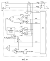
- FIG. 9 depicts the virtual remote sensing technique being applied to a linear regulator 120 .
- a conventional linear regulator comprises a pass transistor, in this case a MOSFET 122 , connected between an input voltage Vin and the output terminal 124 .
- An error amplifier 126 is part of a feedback loop that detects a feedback voltage (conventionally the output voltage or a divided output voltage), compares the output to a reference voltage, and outputs a DC signal that controls the conductivity of the MOSFET 122 to cause the feedback voltage to substantially equal the reference voltage.
- the virtual remote sensing technique of the present invention is applied to the linear regulator in generally the same way as it is applied to a switching regulator, and many different circuits and algorithms can be used to implement the virtual remote sensing technique. Such circuits are represented by the functional blocks 128 and 130 .
- a state machine or other controller initially causes the block 128 to place the regulator 120 in a normal regulator mode.
- the regulator 120 will then generate a current to create a Vout that matches a certain reference voltage.
- the state machine triggers the interrogation mode of block 128 , which sends a signal to the error amplifier 126 , or uses another technique, to increase or decrease the regulator output current by a known fractional amount.
- a load capacitor 134 at the load 132 , and the load capacitor 134 acts as a low impedance to the AC signal.
- Block 130 detects the fractional change in the voltage (or current depending on the technique used) due to the line resistance and scales this fractional change to derive a signal related to the actual full voltage drop at the full load current.
- This correctional voltage signal is then applied to the linear regulator, such as by adjusting the reference voltage or the feedback voltage, to increase the current output of the regulator above what it would have been without the compensation to compensate for the line voltage drop.
- the voltage output of the regulator can instead be varied to detect a fractional change in current and thus derive the line resistance and a compensation signal.
- FIG. 10 illustrates simplified waveforms of the output of a regulator when the regulator is controlled to vary its output voltage between V 1 and V 2 (50% of time at each voltage).
- the average voltage output is VDC.
- the current at the output of the regulator will vary between I 1 and I 2 , with the average current to the load being IDC.
- the load capacitor filters out the dither signal.
- VL is the voltage at the load that has been smoothed by the load capacitor.
- RUNE is the resistance of each line leading to the load.
- VDC VL +(2 *R LINE* IDC ) (Eq. 1)
- VDC VL +[( V 1 ⁇ V 2)*( I 1 +I 2)]/2( I 1 ⁇ I 2) (Eq. 4)
- VL voltage at the load
- that value e.g., 3 volts
- the compensation voltage that needs to be added to the regulator's feedback loop is [(V 1 ⁇ V 2 )*(I 1 +I 2 )]/2(I 1 ⁇ I 2 ).
- Effectively adding this compensation value can be done in many ways.
- One such way is shown in FIG. 11 .
- the regulator 140 may be a switching regulator, a linear regulator, or any other type of regulator that uses a feedback pin.
- the regulator 140 is receiving a feedback signal at its Vc pin 142 that causes it to output V 1 in FIG. 10 .
- the Vc pin is a standard pin that normally is the output of an internal error amplifier, and the voltage at the Vc pin is directly related to the duty cycle (for a switching regulator) or the pass transistor's conductivity (for a linear regulator).
- An integrating capacitor (not shown) is coupled to the Vc pin.
- the circuitry of FIG. 11 bypasses any internal feedback circuitry in the regulator 140 .
- the feedback signal that causes the regulator to output V 1 is due to the state machine 144 controlling the voltage reference 146 to apply the REF 1 to the summer 148 .
- the instantaneous Vout near the output of the regulator 140 is applied to the input of the differential amplifier 150 (a transconductance amplifier) along with the output of the summer 148 .
- the output of amplifier 150 may be connected to an integrating capacitor to create the feedback signal for the regulator 140 .
- the regulator output voltage V 1 results in the current I 1 through the low value sense resistor Rs, and this Rs voltage drop is converted into a representative I 1 signal by the differential amplifier 152 .
- the state machine 144 controls a sample and hold circuit 154 to store this I 1 signal. At the same time, the state machine 144 controls the sample and hold circuit 156 to store the output voltage V 1 .
- the state machine 144 then controls the voltage reference 146 to switch the reference voltage to REF 2 , which changes the Vc pin 142 signal to cause the regulator 140 to reduce the output voltage to V 2 ( FIG. 10 ) and the output current to I 2 .
- the state machine 144 then controls the sample and hold circuits 158 and 160 to hold the values I 2 and V 2 , respectively.
- the differential amplifier 161 outputs a value corresponding to I 1 ⁇ I 2 ; the summer 162 outputs a value corresponding to I 1 +I 2 ; and the differential amplifier 164 outputs a value corresponding to V 1 ⁇ V 2 .
- a multiplier/divider circuit 166 is configured to perform the equation K*[(V 1 ⁇ V 2 )*(I 1 +I 2 )]/(I 1 ⁇ I 2 ) (from equation 4 above) to derive a compensation voltage.
- the factor K is a multiplier for scaling the various values to take into consideration the various gains of the other circuitry, the 2 in the denominator of equation 4, and other factors, so that the output of the multiplier/divider circuit 164 is the actual compensation voltage.
- the state machine 144 controls a sample and hold circuit 168 to hold this compensation voltage, and the capacitor 170 smoothes variations in this signal.
- the derived compensation voltage is then added to the reference voltage (REF 1 or REF 2 ) by summer 148 to offset the reference voltage by the compensation voltage.
- the feedback network modifies the regulator duty cycle (if a switching regulator) or conductivity (if a linear regulator) to cause the voltages at the inputs of the differential amplifier 150 to be substantially equal. As a result, the output of the regulator 140 is effectively augmented by the compensation voltage equal to the voltage drops across the lines leading to the load 174 .
- the virtual remote sensing circuitry basically performs mathematical operations.
- the circuitry for the virtual remote sensor can instead be a programmed digital signal processor (DSP) that carries out the algorithms described herein.
- DSP digital signal processor
- FIG. 12 shows a virtual remote sensing circuit 180 .
- the output voltage and current of the regulator 140 are sensed by any means and converted into digital signals by an analog-to-digital converter 182 .
- the DSP 184 then performs the various algorithms on the digital signal, as previously described, for generating a digital signal that periodically varies the regulator output for performing the line voltage drop/resistance interrogation, and then generates a compensation signal for the feedback loop to compensate for the line voltage drop.
- the digital output of the DSP 184 is then converted into a compensated analog feedback signal by a digital-to-analog converter 186 for controlling the regulator's 140 output voltage.
- the virtual remote sense circuit bypasses the internal feedback circuit of the regulator chip.
- the inventive circuit can be connected to an external pin of the regulator chip (e.g., the Vc pin) or be connected to a suitable terminal of any regulator circuit.
- the bypassed feedback circuitry in a regulator chip is disabled.
- a voltage feedback pin of a conventional regulator chip may be connected to a fixed signal so that the internal circuitry only generates a fixed signal that is offset by the inventive circuit.
- the internal error amplifier in a typical regulator chip will output a fixed current at the Vc pin
- the output of the virtual remote sense circuit connected to the Vc pin can be an open-drain MOSFET connected between the Vc pin and ground.
- the MOSFET is controlled by the virtual sense circuit to siphon off the excess “error” current to cause the feedback voltage to match the compensated reference voltage, or to control the output of the regulator during the test phase.
- the regulator is custom designed to incorporate the inventive circuitry (as a single chip or formed of discrete components) so no circuitry needs to be bypassed.
- the inventive circuit is in a separate chip that can be used with any type of regulator (e.g., voltage mode, current mode, step-up, step-down, etc.).
- the inventive circuit is a separate IC incorporated in the same package as a regulator controller chip.
- any circuit described herein can be optically isolated from the lines and/or regulator by inserting a conventional optical isolator between the feedback circuit and the lines and/or between the feedback circuit and the regulator.
- the circuit can also be DC isolated from the regulator controller chip by connecting a transformer between the switching transistors and the load and connecting the feedback circuit downstream from the transformer.
- the frequency of the interrogation mode can be varied within a range using conventional spread spectrum techniques.
- a beat frequency would be too low to be filtered out by the load capacitor, so such a spread spectrum technique may be important to ensure the load is not adversely affected by the virtual remote sense operation.
- One way to vary the interrogation frequency is to use a pseudo noise generator, which essentially randomizes the frequency within a defined range by controlling a delay circuit that initiates the interrogation mode.
- a soft-start circuit may be used to effectively delay the use of the derived compensation signal until a steady state condition.
- FIG. 13 illustrates a soft-start circuit that effectively blocks the compensation signal from affecting the operation of the regulator until a steady state condition has been reached.
- the compensation signal may, for example, be a correction to a reference voltage used by an error amplifier in the feedback path of the regulator.
- Chold 4 the output of the soft-start circuit is labeled Chold 4 .
- Chold 4 is connected to an external capacitor and the voltage on Chold 4 is applied to an error amplifier in the feedback loop to set the regulator DC output voltage. A feedback voltage is applied to the other input of the error amplifier.
- Chold 4 represents the compensated reference voltage previously described.
- XBGRDY bandgap ready bar
- XPRECHG Low
- XPRECHG High
- Chold 4 is now driven by a current source M 6 , controlled by a first hysteretic comparator output OK 1 , or by a current sink M 22 , controlled by a second hysteretic comparator output OK 2 .
- OK 1 and OK 2 causes the XOK signal to toggle the flip flop (comprising AND gates U 13 /U 15 ), disconnecting the current sources from Chold 4 , and connecting IAMP_OUT to Chold 4 , forcing full line drop voltage correction.
- an automatic voltage compensation circuit has been described using virtual remote sensing of a voltage drop along lines leading to a load.
- Various related techniques may be employed using the same sampling and fractional voltage drop concepts described herein, and such techniques are contemplated by the present invention.
- the remote load may be any device, such as a laptop computer receiving power from a plug-in AC-to-DC adapter via long wires, a power over Ethernet system, a remote regulator receiving an input voltage from another power supply regulator, a battery receiving a charging current from a charger, or any other load.
Landscapes
- Engineering & Computer Science (AREA)
- Power Engineering (AREA)
- Continuous-Control Power Sources That Use Transistors (AREA)
Abstract
Description
VDC=VL+(2*RLINE*IDC) (Eq. 1)
2*RLINE=(V1−V2)*(I1−I2) (Eq. 2)
IDC=(I1+I2)/2 (Eq. 3)
VDC=VL+[(V1−V2)*(I1+I2)]/2(I1−I2) (Eq. 4)
Claims (34)
Priority Applications (1)
| Application Number | Priority Date | Filing Date | Title |
|---|---|---|---|
| US12/610,190 US8754622B2 (en) | 2009-10-30 | 2009-10-30 | Voltage regulator compensating for voltage drop along conductors between regulator output and load |
Applications Claiming Priority (1)
| Application Number | Priority Date | Filing Date | Title |
|---|---|---|---|
| US12/610,190 US8754622B2 (en) | 2009-10-30 | 2009-10-30 | Voltage regulator compensating for voltage drop along conductors between regulator output and load |
Publications (2)
| Publication Number | Publication Date |
|---|---|
| US20110101937A1 US20110101937A1 (en) | 2011-05-05 |
| US8754622B2 true US8754622B2 (en) | 2014-06-17 |
Family
ID=43924692
Family Applications (1)
| Application Number | Title | Priority Date | Filing Date |
|---|---|---|---|
| US12/610,190 Active 2032-12-06 US8754622B2 (en) | 2009-10-30 | 2009-10-30 | Voltage regulator compensating for voltage drop along conductors between regulator output and load |
Country Status (1)
| Country | Link |
|---|---|
| US (1) | US8754622B2 (en) |
Cited By (23)
| Publication number | Priority date | Publication date | Assignee | Title |
|---|---|---|---|---|
| US9448576B2 (en) | 2014-02-17 | 2016-09-20 | Commscope Technologies Llc | Programmable power supplies for cellular base stations and related methods of reducing power loss in cellular systems |
| US9759880B2 (en) | 2013-09-17 | 2017-09-12 | Commscope Technologies Llc | Capacitive-loaded jumper cables, shunt capacitance units and related methods for enhanced power delivery to remote radio heads |
| MD1220Y (en) * | 2017-05-03 | 2017-12-31 | ИНСТИТУТ ЭЛЕКТРОННОЙ ИНЖЕНЕРИИ И НАНОТЕХНОЛОГИЙ "D. Ghitu" АНМ | Process for electric power supply of a remote load |
| US9891646B2 (en) | 2015-01-27 | 2018-02-13 | Qualcomm Incorporated | Capacitively-coupled hybrid parallel power supply |
| US9899921B1 (en) * | 2017-02-01 | 2018-02-20 | Linear Technology Corporation | Adaptive slope compensation for current mode switching power supply |
| US20180164355A1 (en) | 2014-02-17 | 2018-06-14 | Commscope Technologies Llc | Methods and equipment for reducing power loss in cellular systems |
| US10191093B2 (en) | 2015-06-30 | 2019-01-29 | Hanchett Entry Systems, Inc. | Device for measuring voltage across a remote load |
| US10216249B2 (en) | 2016-09-27 | 2019-02-26 | Cisco Technology, Inc. | Electrical power control and fault protection |
| US10224944B2 (en) * | 2017-02-03 | 2019-03-05 | The Regents Of The University Of California | Successive approximation digital voltage regulation methods, devices and systems |
| US10239407B2 (en) | 2016-01-25 | 2019-03-26 | Ford Global Technologies, Llc | Variable carrier switching frequency control of variable voltage converter |
| US10281939B2 (en) | 2014-02-17 | 2019-05-07 | Commscope Technologies Llc | Methods and equipment for reducing power loss in cellular systems |
| US10429604B2 (en) | 2015-11-03 | 2019-10-01 | Raycap S.A. | Modular fiber optic cable splitter |
| US10712515B2 (en) | 2013-09-17 | 2020-07-14 | Commscope Technologies Llc | Capacitive-loaded jumper cables, shunt capacitance units and related methods for enhanced power delivery to remote radio heads |
| US10802237B2 (en) | 2015-11-03 | 2020-10-13 | Raycap S.A. | Fiber optic cable management system |
| US10812664B2 (en) | 2017-01-20 | 2020-10-20 | Raycap S.A. | Power transmission system for wireless communication systems |
| US10971928B2 (en) | 2018-08-28 | 2021-04-06 | Raycap Ip Assets Ltd | Integrated overvoltage protection and monitoring system |
| WO2021090304A1 (en) | 2019-11-04 | 2021-05-14 | Elbit Systems Land And C4I Ltd. | Signal crosstalk suppression on a common wire |
| US11095212B2 (en) * | 2018-09-12 | 2021-08-17 | Vertiv Corporation | Line loss compensating power supplies |
| US11251608B2 (en) | 2010-07-13 | 2022-02-15 | Raycap S.A. | Overvoltage protection system for wireless communication systems |
| US11333695B2 (en) | 2014-02-17 | 2022-05-17 | Commscope Technologies Llc | Methods and equipment for reducing power loss in cellular systems |
| US11677164B2 (en) | 2019-09-25 | 2023-06-13 | Raycap Ip Assets Ltd | Hybrid antenna distribution unit |
| US11818518B2 (en) | 2019-05-01 | 2023-11-14 | Commscope Technologies Llc | Methods and equipment for reducing power loss in cellular systems |
| US12237134B2 (en) | 2021-12-28 | 2025-02-25 | Raycap Ip Assets Ltd | Circuit protection for hybrid antenna distribution units |
Families Citing this family (33)
| Publication number | Priority date | Publication date | Assignee | Title |
|---|---|---|---|---|
| JP5118940B2 (en) * | 2007-11-02 | 2013-01-16 | ローム株式会社 | Power supply |
| US8803497B2 (en) * | 2010-01-07 | 2014-08-12 | Mitsubishi Electric Corporation | Current detector of inductive load |
| US9531190B2 (en) * | 2011-04-15 | 2016-12-27 | The Boeing Company | Bi-directional converter voltage controlled current source for voltage regulation |
| TWI439837B (en) * | 2011-08-26 | 2014-06-01 | Richtek Technology Corp | Voltage regulator controller |
| TWI451224B (en) | 2011-12-21 | 2014-09-01 | Anpec Electronics Corp | Dynamic voltage adjustment device and power transmission system using the same |
| EP2648012A1 (en) * | 2012-04-06 | 2013-10-09 | Dialog Semiconductor GmbH | On-chip test technique for low drop-out regulators, comprising finite state machine |
| US9219415B2 (en) * | 2012-09-27 | 2015-12-22 | Asahi Kasei Microdevices Corporation | Switching power supply circuit |
| US9209690B2 (en) * | 2012-10-01 | 2015-12-08 | Cirel Systems Private Limited | Spread-spectrum switching regulator for eliminating modulation ripple |
| US9377794B1 (en) * | 2012-10-15 | 2016-06-28 | Linear Technology Corporation | Rapid power up of Power Over Ethernet equipment system |
| TWI498704B (en) * | 2012-11-06 | 2015-09-01 | 泰達電子公司 | Power converter capable of dynamically adjusting output voltage and its applicable power supply system |
| US10013003B2 (en) | 2012-11-16 | 2018-07-03 | Linear Technology Corporation | Feed forward current mode switching regulator with improved transient response |
| US10802520B2 (en) * | 2013-04-12 | 2020-10-13 | Keithley Instruments, Llc | High performance current source power supply |
| TWI510877B (en) | 2013-10-23 | 2015-12-01 | Ind Tech Res Inst | Voltage compensation circuit and control method thereof |
| CN103698578A (en) * | 2013-12-26 | 2014-04-02 | 浙江华立科技有限公司 | Power output control method of automatic electric power meter reading system and automatic electric power meter reading system |
| EP2922193A1 (en) * | 2014-03-20 | 2015-09-23 | Panasonic Intellectual Property Management Co., Ltd. | Power conversion apparatus and control method for power conversion apparatus |
| US9509157B2 (en) * | 2014-04-18 | 2016-11-29 | Getac Technology Corporation | Power bank device and current-output method thereof |
| EP2977848B1 (en) * | 2014-07-23 | 2018-02-14 | DET International Holding Limited | Impedance compensation |
| CN105322587B (en) * | 2014-07-28 | 2019-02-26 | 神讯电脑(昆山)有限公司 | Mobile power supply device and current output method thereof |
| JP6090275B2 (en) * | 2014-09-25 | 2017-03-08 | 株式会社デンソー | Power converter |
| WO2016064492A1 (en) * | 2014-10-20 | 2016-04-28 | Ambiq Micro, Inc. | Adaptive voltage converter |
| TWI566069B (en) * | 2015-06-08 | 2017-01-11 | 宏碁股份有限公司 | Power supply device with wire voltage drop compensation |
| CN106325343B (en) * | 2015-06-18 | 2017-11-28 | 宏碁股份有限公司 | Power supply device with wire voltage drop compensation |
| CN106505650B (en) * | 2015-09-07 | 2020-10-23 | 神讯电脑(昆山)有限公司 | Power supply and power control method thereof |
| US20170271981A1 (en) * | 2015-09-29 | 2017-09-21 | Telefonaktiebolaget Lm Ericsson (Publ) | Voltage control in a converter supplying power to a load |
| US9929651B2 (en) * | 2015-11-18 | 2018-03-27 | Microsemi Corporation | Converter with hysteretic control |
| US10003259B2 (en) * | 2016-04-09 | 2018-06-19 | Skyworks Solutions, Inc. | Voltage converter and control method thereof |
| KR101822280B1 (en) * | 2016-05-04 | 2018-01-26 | 현대자동차주식회사 | Method for correcting output voltage sensing error of low voltage dc-dc converter |
| US10551859B2 (en) * | 2016-05-17 | 2020-02-04 | Texas Instruments Incorporated | Methods and apparatus for overshoot, undershoot and delay reduction of a voltage regulator output by dynamically offsetting a reference voltage |
| JP7553769B2 (en) * | 2020-05-19 | 2024-09-19 | ミツミ電機株式会社 | DC-DC converter, semiconductor integrated circuit for power supply control, and power supply device |
| CN111709207B (en) * | 2020-06-11 | 2023-03-28 | 广东浪潮大数据研究有限公司 | Method and device for determining parameters of RC integrator on output inductor of voltage regulator |
| US11791725B2 (en) * | 2020-08-06 | 2023-10-17 | Mediatek Inc. | Voltage regulator with hybrid control for fast transient response |
| US12294295B2 (en) * | 2020-11-23 | 2025-05-06 | Robert S. Wrathall | Systems and methods of unwanted harmonic content removal for power conversion |
| CN113485200A (en) * | 2021-07-30 | 2021-10-08 | 蔚来汽车科技(安徽)有限公司 | Control apparatus, method, mobile equipment and storage medium for electronic device |
Citations (10)
| Publication number | Priority date | Publication date | Assignee | Title |
|---|---|---|---|---|
| US5751139A (en) * | 1997-03-11 | 1998-05-12 | Unitrode Corporation | Multiplexing power converter |
| US5929620A (en) * | 1996-11-07 | 1999-07-27 | Linear Technology Corporation | Switching regulators having a synchronizable oscillator frequency with constant ramp amplitude |
| US6894461B1 (en) * | 2002-10-11 | 2005-05-17 | Linear Technology Corp. | Bidirectional power conversion with multiple control loops |
| US20050243894A1 (en) * | 2004-04-29 | 2005-11-03 | Yuhui Chen | Methods and circuits for frequency modulation that reduce the spectral noise of switching regulators |
| US7170195B2 (en) * | 2004-10-08 | 2007-01-30 | Linear Technology Corporation | Circuits and methods for flexible current partitioning in monolithic switching regulators |
| US20070236201A1 (en) * | 2006-04-05 | 2007-10-11 | James Steven Brown | Correction circuit for improved load transient response |
| US7358532B2 (en) * | 2005-08-03 | 2008-04-15 | Seiko Epson Corporation | Electro-optical device and electronic apparatus |
| US7518351B2 (en) * | 2005-05-18 | 2009-04-14 | Linear Technology Corporation | Switching regulator over voltage reduction circuit and method |
| US7714547B2 (en) * | 2008-08-08 | 2010-05-11 | Semtech Corporation | Method and apparatus for constant on-time switch mode converters |
| US20100253307A1 (en) * | 2009-04-07 | 2010-10-07 | System General Corp. | Pfc converter having two-level output voltage without voltage undershooting |
-
2009
- 2009-10-30 US US12/610,190 patent/US8754622B2/en active Active
Patent Citations (11)
| Publication number | Priority date | Publication date | Assignee | Title |
|---|---|---|---|---|
| US5929620A (en) * | 1996-11-07 | 1999-07-27 | Linear Technology Corporation | Switching regulators having a synchronizable oscillator frequency with constant ramp amplitude |
| US5751139A (en) * | 1997-03-11 | 1998-05-12 | Unitrode Corporation | Multiplexing power converter |
| US6894461B1 (en) * | 2002-10-11 | 2005-05-17 | Linear Technology Corp. | Bidirectional power conversion with multiple control loops |
| US7348767B2 (en) * | 2002-10-11 | 2008-03-25 | Linear Technology Corporation | Bidirectional power conversion with multiple control loops |
| US20050243894A1 (en) * | 2004-04-29 | 2005-11-03 | Yuhui Chen | Methods and circuits for frequency modulation that reduce the spectral noise of switching regulators |
| US7170195B2 (en) * | 2004-10-08 | 2007-01-30 | Linear Technology Corporation | Circuits and methods for flexible current partitioning in monolithic switching regulators |
| US7518351B2 (en) * | 2005-05-18 | 2009-04-14 | Linear Technology Corporation | Switching regulator over voltage reduction circuit and method |
| US7358532B2 (en) * | 2005-08-03 | 2008-04-15 | Seiko Epson Corporation | Electro-optical device and electronic apparatus |
| US20070236201A1 (en) * | 2006-04-05 | 2007-10-11 | James Steven Brown | Correction circuit for improved load transient response |
| US7714547B2 (en) * | 2008-08-08 | 2010-05-11 | Semtech Corporation | Method and apparatus for constant on-time switch mode converters |
| US20100253307A1 (en) * | 2009-04-07 | 2010-10-07 | System General Corp. | Pfc converter having two-level output voltage without voltage undershooting |
Cited By (48)
| Publication number | Priority date | Publication date | Assignee | Title |
|---|---|---|---|---|
| US11251608B2 (en) | 2010-07-13 | 2022-02-15 | Raycap S.A. | Overvoltage protection system for wireless communication systems |
| US9964722B2 (en) | 2013-09-17 | 2018-05-08 | Commscope Technologies Llc | Capacitive-loaded jumper cables, shunt capacitance units and related methods for enhanced power delivery to remote radio heads |
| US9759880B2 (en) | 2013-09-17 | 2017-09-12 | Commscope Technologies Llc | Capacitive-loaded jumper cables, shunt capacitance units and related methods for enhanced power delivery to remote radio heads |
| US10712515B2 (en) | 2013-09-17 | 2020-07-14 | Commscope Technologies Llc | Capacitive-loaded jumper cables, shunt capacitance units and related methods for enhanced power delivery to remote radio heads |
| US10317634B2 (en) | 2013-09-17 | 2019-06-11 | Commscope Technologies Llc | Capacitive-loaded jumper cables, shunt capacitance units and related methods for enhanced power delivery to remote radio heads |
| US11675381B2 (en) | 2014-02-17 | 2023-06-13 | Commscope Technologies Llc | Apparatuses and related methods for reducing power loss |
| US11256277B2 (en) | 2014-02-17 | 2022-02-22 | Commscope Technologies Llc | Programmable power supplies for cellular base stations and related methods of reducing power loss in cellular systems |
| US10025335B2 (en) | 2014-02-17 | 2018-07-17 | Commscope Technologies Llc | Programmable power supplies for cellular base stations and related methods of reducing power loss in cellular systems |
| US12498749B2 (en) | 2014-02-17 | 2025-12-16 | Outdoor Wireless Networks LLC | Power supplies for cellular base stations and related methods of reducing power loss in cellular systems |
| US12493314B2 (en) | 2014-02-17 | 2025-12-09 | Outdoor Wireless Networks LLC | Voltage conversion techniques |
| US12493313B2 (en) | 2014-02-17 | 2025-12-09 | Outdoor Wireless Networks LLC | Programmable power supplies for cellular base stations and related methods of reducing power loss in cellular systems |
| US12314069B2 (en) | 2014-02-17 | 2025-05-27 | Outdoor Wireless Networks LLC | Methods and equipment for reducing power loss in cellular systems |
| US10281939B2 (en) | 2014-02-17 | 2019-05-07 | Commscope Technologies Llc | Methods and equipment for reducing power loss in cellular systems |
| US12072721B2 (en) | 2014-02-17 | 2024-08-27 | Commscope Technologies Llc | Methods and equipment for reducing power loss in cellular systems |
| US10394265B2 (en) | 2014-02-17 | 2019-08-27 | Commscope Technologies Llc | Programmable power supplies for cellular base stations and related methods of reducing power loss in cellular systems |
| US12026000B2 (en) | 2014-02-17 | 2024-07-02 | Commscope Technologies Llc | Methods and equipment for reducing power loss in cellular systems |
| US10423180B2 (en) | 2014-02-17 | 2019-09-24 | Commscope Technologies Llc | Programmable power supplies for cellular base stations and related methods of reducing power loss in cellular systems |
| US11740645B2 (en) | 2014-02-17 | 2023-08-29 | Commscope Technologies Llc | Programmable power supplies for cellular base stations and related methods of reducing power loss in cellular systems |
| US11726508B2 (en) | 2014-02-17 | 2023-08-15 | Commscope Technologies Llc | Methods and systems for determining resistance of power conductors |
| US10782720B2 (en) | 2014-02-17 | 2020-09-22 | Commscope Technologies Llc | Programmable power supplies for cellular base stations and related methods of reducing power loss in cellular systems |
| US9448576B2 (en) | 2014-02-17 | 2016-09-20 | Commscope Technologies Llc | Programmable power supplies for cellular base stations and related methods of reducing power loss in cellular systems |
| US11675382B2 (en) | 2014-02-17 | 2023-06-13 | Commscope Technologies Llc | Programmable power supplies for cellular base stations and related methods of reducing power loss in cellular systems |
| US11669118B2 (en) | 2014-02-17 | 2023-06-06 | Commscope Technologies Llc | Programmable power supplies for cellular base stations and related methods of reducing power loss in cellular systems |
| US11669117B2 (en) | 2014-02-17 | 2023-06-06 | Commscope Technologies Llc | Programmable power supplies for cellular base stations and related methods of reducing power loss in cellular systems |
| US11662759B2 (en) | 2014-02-17 | 2023-05-30 | Commscope Technologies Llc | Programmable power supplies for cellular base stations and related methods of reducing power loss in cellular systems |
| US20180164355A1 (en) | 2014-02-17 | 2018-06-14 | Commscope Technologies Llc | Methods and equipment for reducing power loss in cellular systems |
| US11333695B2 (en) | 2014-02-17 | 2022-05-17 | Commscope Technologies Llc | Methods and equipment for reducing power loss in cellular systems |
| US10830803B2 (en) | 2014-02-17 | 2020-11-10 | Commscope Technologies Llc | Methods and equipment for reducing power loss in cellular systems |
| US11275395B2 (en) | 2014-02-17 | 2022-03-15 | Commscope Technologies Llc | Programmable power supplies for cellular base stations and related methods of reducing power loss in cellular systems |
| US11294409B2 (en) | 2014-02-17 | 2022-04-05 | Commscope Technologies Llc | Methods and equipment for reducing power loss in cellular systems |
| US9891646B2 (en) | 2015-01-27 | 2018-02-13 | Qualcomm Incorporated | Capacitively-coupled hybrid parallel power supply |
| US10416204B2 (en) | 2015-06-30 | 2019-09-17 | Hanchett Entry Systems, Inc. | Device for measuring voltage across a remote load |
| US10191093B2 (en) | 2015-06-30 | 2019-01-29 | Hanchett Entry Systems, Inc. | Device for measuring voltage across a remote load |
| US10429604B2 (en) | 2015-11-03 | 2019-10-01 | Raycap S.A. | Modular fiber optic cable splitter |
| US10802237B2 (en) | 2015-11-03 | 2020-10-13 | Raycap S.A. | Fiber optic cable management system |
| US10239407B2 (en) | 2016-01-25 | 2019-03-26 | Ford Global Technologies, Llc | Variable carrier switching frequency control of variable voltage converter |
| US10216249B2 (en) | 2016-09-27 | 2019-02-26 | Cisco Technology, Inc. | Electrical power control and fault protection |
| US10812664B2 (en) | 2017-01-20 | 2020-10-20 | Raycap S.A. | Power transmission system for wireless communication systems |
| US9899921B1 (en) * | 2017-02-01 | 2018-02-20 | Linear Technology Corporation | Adaptive slope compensation for current mode switching power supply |
| US10224944B2 (en) * | 2017-02-03 | 2019-03-05 | The Regents Of The University Of California | Successive approximation digital voltage regulation methods, devices and systems |
| MD1220Y (en) * | 2017-05-03 | 2017-12-31 | ИНСТИТУТ ЭЛЕКТРОННОЙ ИНЖЕНЕРИИ И НАНОТЕХНОЛОГИЙ "D. Ghitu" АНМ | Process for electric power supply of a remote load |
| US10971928B2 (en) | 2018-08-28 | 2021-04-06 | Raycap Ip Assets Ltd | Integrated overvoltage protection and monitoring system |
| US11095212B2 (en) * | 2018-09-12 | 2021-08-17 | Vertiv Corporation | Line loss compensating power supplies |
| US11818518B2 (en) | 2019-05-01 | 2023-11-14 | Commscope Technologies Llc | Methods and equipment for reducing power loss in cellular systems |
| US12074377B2 (en) | 2019-09-25 | 2024-08-27 | Raycap Ip Assets Ltd | Hybrid antenna distribution unit |
| US11677164B2 (en) | 2019-09-25 | 2023-06-13 | Raycap Ip Assets Ltd | Hybrid antenna distribution unit |
| WO2021090304A1 (en) | 2019-11-04 | 2021-05-14 | Elbit Systems Land And C4I Ltd. | Signal crosstalk suppression on a common wire |
| US12237134B2 (en) | 2021-12-28 | 2025-02-25 | Raycap Ip Assets Ltd | Circuit protection for hybrid antenna distribution units |
Also Published As
| Publication number | Publication date |
|---|---|
| US20110101937A1 (en) | 2011-05-05 |
Similar Documents
| Publication | Publication Date | Title |
|---|---|---|
| US8754622B2 (en) | Voltage regulator compensating for voltage drop along conductors between regulator output and load | |
| US7605574B2 (en) | Switching regulator circuits | |
| US8487593B2 (en) | System and method for detection and compensation of aggressive output filters for switched mode power supplies | |
| US8653413B2 (en) | Welding power supply with digital control of duty cycle | |
| KR100333973B1 (en) | Power Factor Compensation Controller | |
| US8866460B2 (en) | Dynamic dropout control of a power supply | |
| US9048751B2 (en) | Power supply circuit with ripple compensation | |
| US10790737B2 (en) | Current threshold regulation method used in switching converters | |
| US7843178B1 (en) | DC/DC converter startup with frequency ramping | |
| US7489121B2 (en) | Compensation offset adjustment scheme for fast reference voltage transitioning | |
| KR20200040673A (en) | Switched mode power supply with pfc burst mode control | |
| US6011382A (en) | Circuit and method for directly regulating the output voltage of an electroluminescent lamp driver | |
| EP3518407B1 (en) | An apparatus and method for linearization of the control inputs for a dual output resonant converter | |
| US9041468B2 (en) | Switched-mode power supply and method of operation | |
| US20090267573A1 (en) | Power Supplies, Power Supply Controllers, And Power Supply Controlling Methods | |
| JP2009011147A (en) | Switching power supply | |
| TW201346481A (en) | System and method of balanced slope compensation for switch mode regulators | |
| US10175278B1 (en) | Detecting value of output capacitor in switching regulator | |
| US6972974B2 (en) | Compensator to achieve constant bandwidth in a switching regulator | |
| US12348136B2 (en) | Apparatus and method for improving adaptive voltage positioning performance of voltage regulator by sensing output capacitor current | |
| US8487597B2 (en) | Controlled power supply and method for pulse load | |
| CN107465355B (en) | Power supply and voltage correction method | |
| US12587082B2 (en) | Dynamic AC droop control for DC-DC regulators | |
| US20060091869A1 (en) | Method of and system for regulating a power supply | |
| US20240072648A1 (en) | Switching control circuit and power factor correction circuit |
Legal Events
| Date | Code | Title | Description |
|---|---|---|---|
| AS | Assignment |
Owner name: LINEAR TECHNOLOGY CORPORATION, CALIFORNIA Free format text: ASSIGNMENT OF ASSIGNORS INTEREST;ASSIGNORS:DOBKIN, ROBERT;HACK, THOMAS P.;CHEN, YUHUI;SIGNING DATES FROM 20091030 TO 20091106;REEL/FRAME:023492/0497 |
|
| STCF | Information on status: patent grant |
Free format text: PATENTED CASE |
|
| MAFP | Maintenance fee payment |
Free format text: PAYMENT OF MAINTENANCE FEE, 4TH YEAR, LARGE ENTITY (ORIGINAL EVENT CODE: M1551) Year of fee payment: 4 |
|
| AS | Assignment |
Owner name: LINEAR TECHNOLOGY LLC, CALIFORNIA Free format text: ASSIGNMENT OF ASSIGNORS INTEREST;ASSIGNOR:LINEAR TECHNOLOGY CORPORATION;REEL/FRAME:058303/0255 Effective date: 20170502 Owner name: ANALOG DEVICES INTERNATIONAL UNLIMITED COMPANY, IRELAND Free format text: ASSIGNMENT OF ASSIGNORS INTEREST;ASSIGNOR:LINEAR TECHNOLOGY LLC;REEL/FRAME:057888/0345 Effective date: 20181105 |
|
| MAFP | Maintenance fee payment |
Free format text: PAYMENT OF MAINTENANCE FEE, 8TH YEAR, LARGE ENTITY (ORIGINAL EVENT CODE: M1552); ENTITY STATUS OF PATENT OWNER: LARGE ENTITY Year of fee payment: 8 |
|
| FEPP | Fee payment procedure |
Free format text: MAINTENANCE FEE REMINDER MAILED (ORIGINAL EVENT CODE: REM.); ENTITY STATUS OF PATENT OWNER: LARGE ENTITY |