US8742403B2 - Xanthene based semiconductor compositions - Google Patents
Xanthene based semiconductor compositions Download PDFInfo
- Publication number
- US8742403B2 US8742403B2 US13/043,206 US201113043206A US8742403B2 US 8742403 B2 US8742403 B2 US 8742403B2 US 201113043206 A US201113043206 A US 201113043206A US 8742403 B2 US8742403 B2 US 8742403B2
- Authority
- US
- United States
- Prior art keywords
- group
- poly
- substituted
- styrene
- unsubstituted
- Prior art date
- Legal status (The legal status is an assumption and is not a legal conclusion. Google has not performed a legal analysis and makes no representation as to the accuracy of the status listed.)
- Active, expires
Links
- 0 C1=CC2=C(C1)C1=CC=C3OC4=C(CC=C4)C4=C3C1=C(/C=C\4)O2.[1*]C.[2*]C.[3*]C.[4*]C Chemical compound C1=CC2=C(C1)C1=CC=C3OC4=C(CC=C4)C4=C3C1=C(/C=C\4)O2.[1*]C.[2*]C.[3*]C.[4*]C 0.000 description 14
- IAQRGUVFOMOMEM-ARJAWSKDSA-N [H]/C(C)=C(\[H])C Chemical compound [H]/C(C)=C(\[H])C IAQRGUVFOMOMEM-ARJAWSKDSA-N 0.000 description 6
- ZQDPJFUHLCOCRG-WAYWQWQTSA-N [H]/C(CC)=C(\[H])CC Chemical compound [H]/C(CC)=C(\[H])CC ZQDPJFUHLCOCRG-WAYWQWQTSA-N 0.000 description 2
- FHQIJLQOLHALJD-UHFFFAOYSA-N C1=CC=C2OC3=C(C=CC=C3)CC2=C1.C1=CC=C2OC3=C(CC2=C1)SC=C3 Chemical compound C1=CC=C2OC3=C(C=CC=C3)CC2=C1.C1=CC=C2OC3=C(CC2=C1)SC=C3 FHQIJLQOLHALJD-UHFFFAOYSA-N 0.000 description 1
- BKNCYZQKIYIKPQ-UHFFFAOYSA-N CB1OC(C)(C)C(C)(C)O1.CB1OCCCO1 Chemical compound CB1OC(C)(C)C(C)(C)O1.CB1OCCCO1 BKNCYZQKIYIKPQ-UHFFFAOYSA-N 0.000 description 1
- JVZSBUSWSLXISY-UHFFFAOYSA-N CC.CC(C)=C(C)c1ccccc1 Chemical compound CC.CC(C)=C(C)c1ccccc1 JVZSBUSWSLXISY-UHFFFAOYSA-N 0.000 description 1
- DDQYPRPPCBDHEB-UHFFFAOYSA-N CC1=C(C)C(C)=C([Y])C1 Chemical compound CC1=C(C)C(C)=C([Y])C1 DDQYPRPPCBDHEB-UHFFFAOYSA-N 0.000 description 1
- XNLZWJBKPMXDLL-UHFFFAOYSA-N CC1=C(C)C(C)=C([Y])C1.CC1=C([Y])CC2=C1OC1=C3C4=C(C=C1)C1CC([Y])=C(C)C1O/C4=C/C=C/23.OC1=CC=CC2=C(O)C=CC=C12 Chemical compound CC1=C(C)C(C)=C([Y])C1.CC1=C([Y])CC2=C1OC1=C3C4=C(C=C1)C1CC([Y])=C(C)C1O/C4=C/C=C/23.OC1=CC=CC2=C(O)C=CC=C12 XNLZWJBKPMXDLL-UHFFFAOYSA-N 0.000 description 1
Images


Classifications
-
- C—CHEMISTRY; METALLURGY
- C07—ORGANIC CHEMISTRY
- C07D—HETEROCYCLIC COMPOUNDS
- C07D493/00—Heterocyclic compounds containing oxygen atoms as the only ring hetero atoms in the condensed system
- C07D493/02—Heterocyclic compounds containing oxygen atoms as the only ring hetero atoms in the condensed system in which the condensed system contains two hetero rings
- C07D493/06—Peri-condensed systems
-
- C—CHEMISTRY; METALLURGY
- C07—ORGANIC CHEMISTRY
- C07D—HETEROCYCLIC COMPOUNDS
- C07D495/00—Heterocyclic compounds containing in the condensed system at least one hetero ring having sulfur atoms as the only ring hetero atoms
- C07D495/22—Heterocyclic compounds containing in the condensed system at least one hetero ring having sulfur atoms as the only ring hetero atoms in which the condensed system contains four or more hetero rings
-
- C—CHEMISTRY; METALLURGY
- C08—ORGANIC MACROMOLECULAR COMPOUNDS; THEIR PREPARATION OR CHEMICAL WORKING-UP; COMPOSITIONS BASED THEREON
- C08K—Use of inorganic or non-macromolecular organic substances as compounding ingredients
- C08K5/00—Use of organic ingredients
- C08K5/04—Oxygen-containing compounds
- C08K5/15—Heterocyclic compounds having oxygen in the ring
- C08K5/151—Heterocyclic compounds having oxygen in the ring having one oxygen atom in the ring
- C08K5/1545—Six-membered rings
-
- C—CHEMISTRY; METALLURGY
- C08—ORGANIC MACROMOLECULAR COMPOUNDS; THEIR PREPARATION OR CHEMICAL WORKING-UP; COMPOSITIONS BASED THEREON
- C08K—Use of inorganic or non-macromolecular organic substances as compounding ingredients
- C08K5/00—Use of organic ingredients
- C08K5/36—Sulfur-, selenium-, or tellurium-containing compounds
- C08K5/45—Heterocyclic compounds having sulfur in the ring
-
- C—CHEMISTRY; METALLURGY
- C08—ORGANIC MACROMOLECULAR COMPOUNDS; THEIR PREPARATION OR CHEMICAL WORKING-UP; COMPOSITIONS BASED THEREON
- C08L—COMPOSITIONS OF MACROMOLECULAR COMPOUNDS
- C08L25/00—Compositions of, homopolymers or copolymers of compounds having one or more unsaturated aliphatic radicals, each having only one carbon-to-carbon double bond, and at least one being terminated by an aromatic carbocyclic ring; Compositions of derivatives of such polymers
- C08L25/02—Homopolymers or copolymers of hydrocarbons
- C08L25/04—Homopolymers or copolymers of styrene
-
- H—ELECTRICITY
- H10—SEMICONDUCTOR DEVICES; ELECTRIC SOLID-STATE DEVICES NOT OTHERWISE PROVIDED FOR
- H10K—ORGANIC ELECTRIC SOLID-STATE DEVICES
- H10K10/00—Organic devices specially adapted for rectifying, amplifying, oscillating or switching; Organic capacitors or resistors having a potential-jump barrier or a surface barrier
- H10K10/40—Organic transistors
- H10K10/46—Field-effect transistors, e.g. organic thin-film transistors [OTFT]
- H10K10/462—Insulated gate field-effect transistors [IGFETs]
- H10K10/464—Lateral top-gate IGFETs comprising only a single gate
-
- H—ELECTRICITY
- H10—SEMICONDUCTOR DEVICES; ELECTRIC SOLID-STATE DEVICES NOT OTHERWISE PROVIDED FOR
- H10K—ORGANIC ELECTRIC SOLID-STATE DEVICES
- H10K10/00—Organic devices specially adapted for rectifying, amplifying, oscillating or switching; Organic capacitors or resistors having a potential-jump barrier or a surface barrier
- H10K10/40—Organic transistors
- H10K10/46—Field-effect transistors, e.g. organic thin-film transistors [OTFT]
- H10K10/462—Insulated gate field-effect transistors [IGFETs]
- H10K10/466—Lateral bottom-gate IGFETs comprising only a single gate
-
- H—ELECTRICITY
- H10—SEMICONDUCTOR DEVICES; ELECTRIC SOLID-STATE DEVICES NOT OTHERWISE PROVIDED FOR
- H10K—ORGANIC ELECTRIC SOLID-STATE DEVICES
- H10K10/00—Organic devices specially adapted for rectifying, amplifying, oscillating or switching; Organic capacitors or resistors having a potential-jump barrier or a surface barrier
- H10K10/40—Organic transistors
- H10K10/46—Field-effect transistors, e.g. organic thin-film transistors [OTFT]
- H10K10/462—Insulated gate field-effect transistors [IGFETs]
- H10K10/484—Insulated gate field-effect transistors [IGFETs] characterised by the channel regions
-
- H—ELECTRICITY
- H10—SEMICONDUCTOR DEVICES; ELECTRIC SOLID-STATE DEVICES NOT OTHERWISE PROVIDED FOR
- H10K—ORGANIC ELECTRIC SOLID-STATE DEVICES
- H10K85/00—Organic materials used in the body or electrodes of devices covered by this subclass
- H10K85/60—Organic compounds having low molecular weight
- H10K85/649—Aromatic compounds comprising a hetero atom
- H10K85/655—Aromatic compounds comprising a hetero atom comprising only sulfur as heteroatom
-
- H—ELECTRICITY
- H10—SEMICONDUCTOR DEVICES; ELECTRIC SOLID-STATE DEVICES NOT OTHERWISE PROVIDED FOR
- H10K—ORGANIC ELECTRIC SOLID-STATE DEVICES
- H10K85/00—Organic materials used in the body or electrodes of devices covered by this subclass
- H10K85/60—Organic compounds having low molecular weight
- H10K85/649—Aromatic compounds comprising a hetero atom
- H10K85/657—Polycyclic condensed heteroaromatic hydrocarbons
-
- Y—GENERAL TAGGING OF NEW TECHNOLOGICAL DEVELOPMENTS; GENERAL TAGGING OF CROSS-SECTIONAL TECHNOLOGIES SPANNING OVER SEVERAL SECTIONS OF THE IPC; TECHNICAL SUBJECTS COVERED BY FORMER USPC CROSS-REFERENCE ART COLLECTIONS [XRACs] AND DIGESTS
- Y02—TECHNOLOGIES OR APPLICATIONS FOR MITIGATION OR ADAPTATION AGAINST CLIMATE CHANGE
- Y02E—REDUCTION OF GREENHOUSE GAS [GHG] EMISSIONS, RELATED TO ENERGY GENERATION, TRANSMISSION OR DISTRIBUTION
- Y02E10/00—Energy generation through renewable energy sources
- Y02E10/50—Photovoltaic [PV] energy
- Y02E10/549—Organic PV cells
-
- Y—GENERAL TAGGING OF NEW TECHNOLOGICAL DEVELOPMENTS; GENERAL TAGGING OF CROSS-SECTIONAL TECHNOLOGIES SPANNING OVER SEVERAL SECTIONS OF THE IPC; TECHNICAL SUBJECTS COVERED BY FORMER USPC CROSS-REFERENCE ART COLLECTIONS [XRACs] AND DIGESTS
- Y02—TECHNOLOGIES OR APPLICATIONS FOR MITIGATION OR ADAPTATION AGAINST CLIMATE CHANGE
- Y02P—CLIMATE CHANGE MITIGATION TECHNOLOGIES IN THE PRODUCTION OR PROCESSING OF GOODS
- Y02P70/00—Climate change mitigation technologies in the production process for final industrial or consumer products
- Y02P70/50—Manufacturing or production processes characterised by the final manufactured product
Definitions
- POE printed organic electronics
- TFT printed thin-film transistor
- TFTs are generally composed of a supporting substrate, three electrically conductive electrodes (gate, source and drain electrodes), a channel semiconductor layer, and an electrically insulating gate dielectric layer separating the gate electrode from the semiconductor layer. It is desirable to improve the performance of known TFTs. Performance can be measured by at least two properties: mobility, and the on/off ratio. Mobility is measured in units of cm 2 /V ⁇ sec; higher mobility is desired. The on/off ratio is the ratio between the amount of current that leaks through the TFT in the off state versus the current that runs through the TFT in the on state. Typically, a higher on/off ratio is more desirable.
- OFTs Organic thin-film transistors
- RFID radio frequency identification
- backplane switching circuits for displays, such as signage, readers, and liquid crystal displays, where high switching speeds and/or high density are not essential. They also have attractive mechanical properties such as being physically compact, lightweight, and flexible.
- the semiconducting layers of OTFTs can be fabricated using low-cost solution-based patterning and deposition techniques, such as spin coating, solution casting, dip coating, stencil/screen printing, flexography, gravure, offset printing, ink jet-printing, micro-contact printing, and the like.
- solution processable materials are therefore required.
- organic or polymeric semiconductors formed by solution processing tend to suffer from limited solubility, air sensitivity, and especially low field-effect mobility. This poor performance may be attributable to the poor film-forming nature of small molecules.
- R 1 , R 2 , R 3 and R 4 are independently selected from a hydrogen atom, a substituted or unsubstituted alkyl group, a substituted or unsubstituted alkenyl group, a substituted or unsubstituted ethynyl group, a substituted or unsubstituted aryl group, a substituted or unsubstituted heteroaryl group, an alkoxy group, an alkylthio group, an alkylsilyl group, a cyano group, and a halogen atom, wherein n is 1 or 2, and wherein X is independently S or
- a semiconductor composition comprising: a polymer binder; and a small molecule semiconductor of Formula (I):
- R 1 , R 2 , R 3 and R 4 are independently selected from a hydrogen atom, a substituted or unsubstituted alkyl group, a substituted or unsubstituted alkenyl group, a substituted or unsubstituted ethynyl group, a substituted or unsubstituted aryl group, a substituted or unsubstituted heteroaryl group, an alkoxy group, an alkylthio group, an alkylsilyl group, a cyano group, and a halogen atom, wherein n is 1 or 2, and wherein X is independently S or
- an electronic device comprising a semiconducting layer, the semiconducting layer comprising: a small molecule semiconductor of Formula (I):
- R 1 , R 2 , R 3 and R 4 are independently selected from a hydrogen atom, a substituted or unsubstituted alkyl group, a substituted or unsubstituted alkenyl group, a substituted or unsubstituted ethynyl group, a substituted or unsubstituted aryl group, a substituted or unsubstituted heteroaryl group, an alkoxy group, an alkylthio group, an alkylsilyl group, a cyano group, and a halogen atom, wherein n is 1 or 2, and wherein X is independently S or
- FIGS. 1 and 2 illustrate various representative embodiments of the present disclosure, wherein small molecule semiconductors of the formulas as illustrated herein are selected as the semiconductor material in thin-film transistor (TFT) configurations.
- TFT thin-film transistor
- FIG. 3 shows a color model of the equilibrium geometry and simulated crystal structure of 2,8-bis(5-hexylthiophen-2-yl)thieno[3′,2′:2,3]chromeno[6,5,4-def]thieno[3,2-b]chromene.
- the present disclosure relates to small molecule semiconductor compounds having a fused xanthene core as disclosed herein.
- Compositions comprising a polymer binder and the small molecule semiconductor are also disclosed.
- a semiconducting layer formed from the composition is very stable in air and has high mobility.
- These semiconductor compositions are useful for forming layers, such as semiconducting layers, in electronic devices, such as thin film transistors (TFTs).
- Xanthene based semiconducting compounds are important materials for organic thin-film transistors and organic polymer solar cells. “Xanthene based” is defined herein as materials possessing at least one oxaanthracene subunit or at least one thienochromoene subunit in the semiconductor core. The chemical formulas of oxaanthracene and thienochromene are shown below.
- This material is soluble (allowing for ease of use in manufacturing) and exhibits high field-effect mobility in TFTs without requiring a thermal annealing step during device fabrication.
- soluble xanthene based semiconducting compounds may include a small molecule semiconductor having the structure of Formula (I):
- R 1 , R 2 , R 3 and R 4 are independently selected from a hydrogen atom, a substituted or unsubstituted alkyl group, a substituted or unsubstituted alkenyl group, a substituted or unsubstituted ethynyl group, a substituted or unsubstituted aryl group, a substituted or unsubstituted heteroaryl group, an alkoxy group, an alkylthio group, an alkylsilyl group, and a heteroatom, such as a halogen atom, wherein n is 1 or 2, and wherein X is independently S or
- small molecule is defined herein as a compound having a molecular weight less than about 1500 Daltons, such as less than about 1000 Daltons.
- substituted refers to at least one hydrogen atom on the named radical being substituted with another functional group, such as halogen, —CN, —NO 2 , —COOH, and —SO 3 H.
- An exemplary substituted alkyl group is a perhaloalkyl group, wherein one or more hydrogen atoms in an alkyl group are replaced with halogen atoms, such as fluorine, chlorine, iodine, and bromine.
- an aryl group may also be substituted with alkyl, alkoxy, or alkylthio.
- Exemplary substituted aryl groups include propylphenyl and propoxyphenyl.
- alkyl refers to a radical composed entirely of carbon atoms and hydrogen atoms that is fully saturated and of the formula —C n H 2n+1 .
- the alkyl radical may be linear, branched, or cyclic, and contain from about 3 to about 50 carbon atoms, from about 4 to about 40 carbon atoms, from about 5 to about 36 carbon atoms and from about 8 to about 24 carbon atoms.
- alkenyl refers to a radical that contains at least one carbon-carbon double bond that is not part of an aryl or heteroaryl structure.
- the alkenyl radical may be linear, branched, or cyclic, and may include heteroatoms.
- Exemplary alkenyl radicals include arylalkenyl radicals like 2-phenylethenyl or 2-naphthylethenyl; and heteroarylalkenyl radicals like 2-thienylethenyl.
- ethynyl refers to a radical composed entirely of carbon atoms and hydrogen atoms that contains at least one carbon-carbon triple bond.
- aryl refers to an aromatic radical composed entirely of carbon atoms and hydrogen atoms. When aryl is described in connection with a numerical range of carbon atoms, it should not be construed as including substituted aromatic radicals.
- aryl containing from 6 to 10 carbon atoms should be construed as referring to a phenyl group (6 carbon atoms) or a naphthyl group (10 carbon atoms) only, and should not be construed as including a methylphenyl group (7 carbon atoms).
- the aryl group may be substituted with additional substituents such as an alkyl group, an alkoxy group, an alkylthio group, a cyano group and a halogen.
- heteroaryl refers to an aromatic radical composed of carbon atoms, hydrogen atoms, and one or more heteroatoms.
- the carbon atoms and the heteroatoms are present in a cyclic ring or backbone of the radical.
- the heteroatoms are selected from O, S, and N.
- Exemplary heteroaryl radicals include thienyl and pyridinyl.
- alkoxy refers to an alkyl radical, which is attached to an oxygen atom, such as —O—C n H 2n+1 , wherein n is from 1 to 30, from 3 to 24, from 3 to 16 and from 6 to 16.
- alkylthio refers to an alkyl radical that is attached to a sulfur atom, i.e. —S—C n H 2n+1 , wherein n is from 1 to 30, from 3 to 24, from 3 to 16 and from 6 to 16.
- alkylsilyl refers to a radical composed of a tetravalent silicon atom having three alkyl radicals attached to the silicon atom, i.e. —Si(R) 3 , wherein R is an alkyl as defined.
- the three alkyl radicals may be the same or different.
- the alkyl and alkoxy groups each independently contain from 1 to 30 carbon atoms.
- the aryl and heteroaryl groups independently contain from 4 to 30 carbon atoms.
- X in the same molecule may be the same or different.
- X of Formula (I) may be a sulfur atom (S) or
- the small molecule semiconductor have a xanthene core may be fused with a thiophene, benzene or a naphthalene. Specific examples include those shown in Formulas (I-a) through (I-d):
- R 1 , R 2 , R 3 and R 4 are independently selected from a hydrogen atom, a substituted or unsubstituted alkyl group, a substituted or unsubstituted alkenyl group, a substituted or unsubstituted ethynyl group, a substituted or unsubstituted aryl group, a substituted or unsubstituted heteroaryl group, an alkoxy group, an alkylthio group, an alkylsilyl group, and a halogen atom.
- the small molecule semiconductor compounds having a fused xanthene core may also be represented by compounds having the structure of formula (II),
- R is independently selected from a hydrogen atom, a substituted or unsubstituted alkyl group, a substituted or unsubstituted alkenyl group, a substituted or unsubstituted ethynyl group, a substituted or unsubstituted aryl group, an alkoxy group, an alkylthio group, an alkylsilyl group, and a halogen atom, and wherein m is from 1 to 10, from 1 to 5 and 1 to 3.
- the small molecule semiconductor has a band gap of from about 1.6 to about 3.0 eV. This large band gap typically means that the small molecule semiconductor has better stability in air, when compared to a pentacene-based semiconductor.
- the small molecule semiconductor has a crystalline or liquid crystalline structure.
- This xanthene semiconductor core can be synthesized, for example, by coupling a dihydroxynaphthalene compound with a dihalogenated arene compound using a palladium catalyzed cross-coupling reaction.
- dihydroxynapthalene compounds such as 1,5-dihydroxynaphthalene, 2,6-dichloro-1,5-dihydroxynaphthalene, and 2,6-dihexyl-1,5-dihydroxynaphthalene.
- halogenated arene compound examples include those compounds represented by Formula (III):
- X is a sulfur (S) or a
- Y and Y′ are a hydrogen atom or fused aromatic ring, such as, for example, a fused benzene ring or a fused thiophene ring, and Z is independently a halogen atom, such as, for example, chlorine, bromine, iodine, fluorine.
- halogenated arene compound may include, but are not limited to, 1,2-dibromobenzene, 1,2-dibromo-5,6-dimethylbenzene, 3,4-dibromotoluene, 2,3-dibromonaphthalene, 2,3-dibromo-6,7-dicyanonaphthalene, 2,3-dibromothiophene, 2,3-dibromo-5-hexylthiophene and 2,3-dibromo[1]benzothiophene.
- the xanthene semiconductor core may be synthesized using palladium cross-coupling techniques. Examples of these techniques include a palladium catalyzed Heck oxy-arylation reaction, wherein a mixture comprised of a substituted or unsubstituted 1,5-dihydroxynapthalene compound and a dihalogenated aromatic compound is treated with a base in the presence of a palladium catalyst and a solvent.
- Example bases include alkali metal bases such as, for example, K 2 CO 3 , Cs 2 CO 3 , KOt-Bu, KF, CsF and K 3 PO 4 .
- Examples of the palladium catalyst may include PdOAc 2 :PPh 3 , PdOAc 2 :Pt-Bu 3 , Pd(PPh 3 ) 4 and Pd(PPh 3 ) 2 Cl 2 .
- Example solvents may be dimethylformamide (DMF), N-methylpyrrolidone (NMP), toluene, xylene and dioxane.
- the reaction is typically heated to a temperature greater than about 100° C., such as, for example, greater than about 150° C. for a period greater than 1 hour, such as, for example, from about 1 hour up to about 24 hours and from about 1 hour to about 12 hours.
- the semiconductors described herein can be prepared using the procedures described in Y.
- X is a sulfur (S) or a
- Y and Y′ are a hydrogen atom or fused aromatic ring, such as, for example, a fused benzene ring or a fused thiophene ring, and Z is independently a halogen atom, such as, for example, chlorine, bromine, iodine, fluorine.
- the small molecule semiconductors described herein can be prepared by first halogenating the benzene-fused or thiophene fused xanthene core.
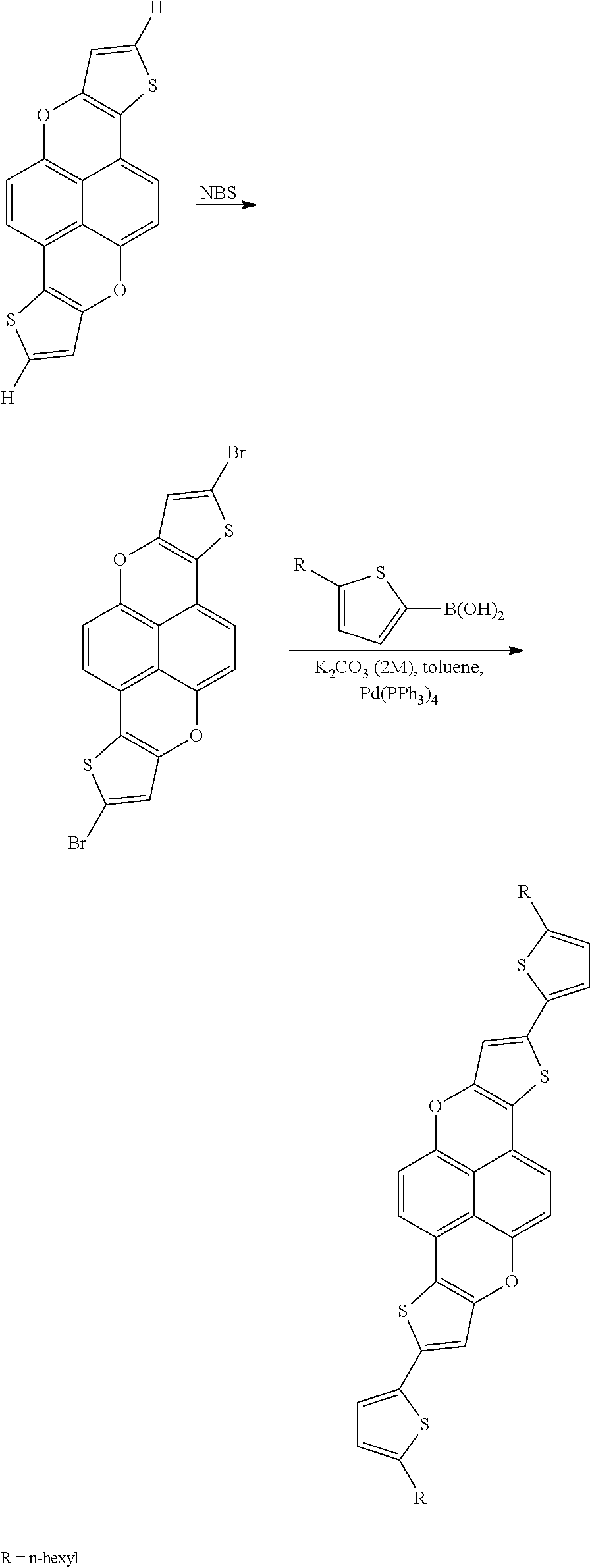
- Suitable halogenating reagents include bromine and N-bromosuccinimide.
- the halogenated xanthene compound is then coupled with a substituted or unsubstituted aryl boronic acid (or ester) or a substituted or unsubstituted heteroaryl boronic acid (or ester).
- aryl boronic acids include phenylboronic acid, 4-propylphenylbornic acid.
- heteroarylboronic acids include 2-thienylboronic acid and 5-hexyl-2-thienylboronic acid. Such reactions are commonly referred to as “Suzuki couplings”.
- the semiconductors described herein can also be prepared by other aryl-aryl coupling reactions, such as Yamamoto coupling, Stille coupling, Ullman coupling, or Heck coupling.
- suitable cross-coupling reactions are described in U.S. Patent Application Pub. No. 2009/0179198, the disclosure of which is incorporated by reference herein in its entirety.
- Other cross-coupling reactions are described in Hou et al., Bandgap and Molecular Energy Level Control of Conjugated Polymer Photovoltaic Materials Based on Benzo[ 1,2- b: 4,5- b′]dithiophene , M ACROMOLECULES, 2008, 41, 6012-6018 and Usta et al.
- R is independently selected from a hydrogen atom, a substituted or unsubstituted alkyl group, a substituted or unsubstituted alkenyl group, a substituted or unsubstituted ethynyl group, a substituted or unsubstituted aryl group, an alkoxy group, an alkylthio group, an alkylsilyl group, and a halogen atom, wherein n is an integer of from about 1 to about 10, from 1 to about 5 and 1 to about 3, and M is a zinc halide, a magnesium halide, SnMe 3 , SnBu 3 , B(OH) 2 , or a cyclic boronic ester having a formula
- the small molecule semiconductor by itself may have poor film-forming properties.
- a semiconductor composition may be formed that comprises the small molecule semiconductor of Formula (I) and a polymer binder. This allows a uniform film to be achieved, significantly improving device performance.
- the polymer binder can be considered as forming a matrix within which the small molecule semiconductor is dispersed.
- the polymer is an amorphous polymer.
- the amorphous polymer may have a glass transition temperature less than the melting point temperature of the small molecule semiconductor. In other embodiments, the amorphous polymer has a glass transition temperature greater than the melting point temperature of the small molecule semiconductor.
- the polymer has a dielectric constant less than 4.5, less than 3.5, including less than 3.0, as measured at 60 Hz at room temperature. In embodiments, the polymer is selected from polymers containing only C, H, F, Cl, or N atoms.
- the polymer is a low polarity polymer, such as a hydrocarbon polymer or a fluorocarbon polymer without any polar groups.
- polystyrene is an amorphous polymer and has a dielectric constant about 2.6.
- a list of other low polarity polymers includes but is not limited to the following: fluoropolyarylether, poly(p-xylylene), poly(vinyl toluene), poly( ⁇ -methyl styrene), poly(vinyl naphthalene), polyethylene, polypropylene, polyisoprene, poly(tetrafluoroethylene), poly(chlorotrifluoroethylene), poly(2-methyl-1,3-butadiene), poly(cyclohexyl methacrylate), poly(chlorostyrene), poly(4-methyl styrene), poly(vinylcyclohexane), polyphenylene, poly-p-phenylvinylidenes, poly(arylene ether), polyisobutylene, poly(2,6-dimethyl-1,4-phenylene ether), poly[1,1-(2-methyl propane) bis-(4-phenyl)carbonate], poly( ⁇ - ⁇ - ⁇ ′- ⁇ ′tetraflu
- Exemplary polymer binders suitable for the semiconductor composition include polystyrene, poly( ⁇ -methyl styrene), poly(4-methyl styrene), poly( ⁇ -methyl styrene-co-vinyl toluene), poly(styrene-block-butadiene-block-styrene), poly(styrene-block-isoprene-block-styrene), poly(vinyl toluene), a terpene resin, poly(styrene-co-2,4-dimethylstyrene), poly(chlorostyrene), poly(styrene-co- ⁇ -methyl styrene), poly(styrene-co-butadiene), polycarbazole, a polytriarylamine, or poly(N-vinylcarbazole).
- a styrene-based polymer in particular, is believed to be a suitable polymer binder.
- Styrene-based polymers contain a repeating unit derived from a styrene monomer of Formula (IV):
- R g , R h , R j , and R k are independently hydrogen, halogen, and C 1 -C 20 alkyl; and n is an integer from 0 to 5.
- the styrene-based polymer may have a weight average molecular weight of from about 40,000 to about 2,000,000, from about 50,000 to about 1,000,000, from about 50,000 to about 500,000 and from about 75,000 to about 250,000.
- the weight ratio of the small molecule semiconductor to the polymer binder may be from 5:1 to 2:3, from 3:1 to 5:6 and 2:1 to 1:1.
- the polymer binder may be present in the semiconductor composition in an amount of from about 0.1 to about 10%, from about 0.1 to about 2%, from about 0.5 to about 2% and from about 0.5 to about 1%.
- the semiconductor composition is soluble or substantially soluble in common coating solvents and thus may form a semiconductor solution comprised of the material in an organic solvent.
- the small molecule semiconductor and/or the polymer binder possess a solubility of at least about 0.1 percent by weight, and more specifically, from about 0.3 percent to about 10 percent, or to about 50 percent by weight in such solvents as chlorinated solvents such as chlorobenzene, chlorotoluene, dichlorobenzene, dichloroethane, and the like; alcohols and diols such as propanol, butanol, hexanol, hexanediol, and the like; hydrocarbons or aromatic hydrocarbons such as hexane, heptane, toluene, xylene, ethyl benzene, and the like; ketones such as acetone, methyl ethyl ketone, and the like.; acetates, such as eth
- the small molecule semiconductors of the formulas as illustrated herein provide a stable conductivity of, for example, from about 10 ⁇ 9 S/cm to about 10 ⁇ 4 S/cm, and more specifically, from about 10 ⁇ 8 S/cm to about 10 ⁇ 5 S/cm as determined by conventional four-probe conductivity measurements.
- the solvent may be present in the semiconductor solution in an amount of from about 50 to about 99.9 wt. %, from about 80 to about 99.5 wt. %, from about 90 to about 99 wt. % and from about 95 to about 99 wt. %, based upon the weight of the semiconductor solution.
- Fabrication of a printed organic electronic (POE) device using the semiconductor solution can be carried out by depositing the semiconductor solution on a substrate using any suitable liquid deposition technique at any suitable time prior to or subsequent to the formation of other optional layer or layers on the substrate.
- liquid deposition of the semiconductor solution on the substrate can occur either on a substrate or on a substrate already containing layered material, for example, a semiconductor layer and/or an insulating layer of a thin-film transistor.
- liquid deposition technique refers to, for example, deposition of a composition using a liquid process such as liquid coating or printing technique, where the liquid is a homogeneous or heterogeneous dispersion of the small molecule semiconductors in a solvent.
- the semiconductor solution may be deposited in any suitable pattern on the substrate.
- liquid coating processes may include, for example, spin coating, blade coating, rod coating, dip coating, and the like.
- printing techniques may include, for example, lithography or offset printing, gravure, flexography, screen printing, stencil printing, inkjet printing, stamping (such as microcontact printing), and the like.
- liquid deposition of the semiconductor solution deposits a layer of the small molecule semiconductor having a thickness ranging from about 5 nanometers to about 5 millimeters, from about 10 nanometers to about 1000 micrometers, from about 100 nanometers to about 500 micrometers, from about 1 micrometer to about 100 micrometers and from about 5 micrometers to about 25 micrometers.
- the deposited semiconductor solution at this stage may or may not exhibit appreciable electrical conductivity.
- the heating temperature is one that does not cause adverse changes in the properties of previously deposited layer(s) or the substrate (whether single layer substrate or multilayer substrate) and the heating temperature is related to the temperature following deposition.
- the heating can be performed for a time ranging from, for example, 1 second to about 10 hours and from about 10 seconds to 1 hour.
- the heating can be performed in air, in an inert atmosphere, for example, under nitrogen or argon, or in a reducing atmosphere, for example, under nitrogen containing from 1 to about 20 percent by volume hydrogen.
- the heating can also be performed under normal atmospheric pressure or at a reduced pressure of, for example, from about 1000 mbars to about 0.01 mbars.
- heating encompasses any technique(s) that can impart sufficient energy to remove the solvent from the substrate.
- heating techniques may include thermal heating (for example, a hot plate, an oven, and a burner), infra-red (“IR”) radiation, a laser beam, microwave radiation, or UV radiation, or a combination thereof.
- the small molecule semiconductor of Formula (1) upon being deposited in a semiconductor layer, may be used in electronic devices such as thin-film transistors (TFT), diodes and photovoltaic devices, such as polymer solar cells (PSCs).
- TFT thin-film transistors
- PSCs polymer solar cells
- a thin-film transistor comprising:
- the substrate layer may generally be a silicon material inclusive of various appropriate forms of silicon, a glass plate, a plastic film or a sheet, and the like depending on the intended applications.
- a plastic substrate such as for example polyester, polycarbonate, polyimide sheets, and the like, may be selected.
- the thickness of the substrate may be, for example, from about 10 micrometers to about 100 millimeters with a specific thickness being from about 50 to about 100 micrometers, especially for a flexible plastic substrate, and from about 1 to about 10 millimeters for a rigid substrate such as glass or silicon.
- the gate dielectric layer which can separate the gate electrode from the source and drain electrodes, and in contact with the semiconductor layer, can generally be an inorganic material film, an organic polymer film, or an organic-inorganic composite film.
- the thickness of the gate dielectric layer can be, for example, from about 10 nanometers to about 1 micrometer with a more specific thickness being about 100 nanometers to about 500 nanometers.
- inorganic materials suitable as the dielectric layer may include silicon oxide, silicon nitride, aluminum oxide, barium titanate, barium zirconate titanate and the like.
- Examples of organic polymers for the dielectric layer may include polyesters, polycarbonates, poly(vinyl phenol), polyimides, polystyrene, poly(methacrylate)s, poly(acrylate)s, epoxy resin and the like.
- Examples of inorganic-organic composite materials may include nanosized metal oxide particles dispersed in polymers, such as polyester, polyimide, epoxy resin and the like.
- the gate dielectric layer is generally of a thickness of from about 50 nanometers to about 500 nanometers depending on the dielectric constant of the dielectric material used.
- the dielectric material has a dielectric constant of, for example, at least about 3, thus a suitable dielectric thickness of about 300 nanometers can provide a desirable capacitance, for example, of about 10 ⁇ 9 to about 10 ⁇ 7 F/cm 2 .
- the dielectric layer may be surface modified with a surface modifier.
- exemplary surface modifiers include organosilanes, such as hexamethyldisilazane (HMDS), phenyltrichlorosilane, octyltrichlorosilane (OTS-8), and octadecyltrichlorosilane (ODTS-18).
- HMDS hexamethyldisilazane
- OTS-8 octyltrichlorosilane
- ODTS-18 octadecyltrichlorosilane
- the active semiconductor layer comprised of small molecule semiconductors of the Formulas as illustrated herein, and wherein the thickness of this layer is generally, for example, about 5 nanometers to about 1 micrometer, about 5 nanometers to about 500 nanometers or about 40 nanometers to about 100 nanometers.
- This layer can generally be fabricated by solution processes such as spin coating, casting, screen, stamp, or jet printing of a solution of small molecule semiconductors of the present disclosure. In certain configurations, the semiconducting layer completely covers the source and drain electrodes.
- the gate electrode can be a thin metal film, a conducting polymer film, a conducting film generated from a conducting ink or paste, or the substrate itself (for example heavily doped silicon).
- the gate electrode materials may include gold, silver, chromium, indium tin oxide, conducting polymers, such as polystyrene sulfonate-doped poly(3,4-ethylenedioxythiophene) (PSS/PEDOT), a conducting ink/paste comprised of carbon black/graphite or colloidal silver dispersion contained in a polymer binder, such as Electrodag available from Acheson Colloids Company, and silver filled electrically conductive thermoplastic ink available from Noelle Industries, and the like.
- the gate layer may be prepared by vacuum evaporation, sputtering of metals or conductive metal oxides, coating from conducting polymer solutions or conducting inks, or dispersions by spin coating, casting or printing.
- the thickness of the gate electrode layer may be, for example, from about 10 nanometers to about 10 micrometers, and a specific thickness may be, for example, from about 10 to about 200 nanometers for metal films, and about 1 to about 10 micrometers for polymer conductors.
- the source and drain electrode layer can be fabricated from materials which provide a low resistance ohmic contact to the semiconductor layer.
- Typical materials suitable for use as source and drain electrodes may include those of the gate electrode materials such as gold, nickel, aluminum, platinum, conducting polymers, and conducting inks.
- Typical thickness of this layer may be, for example, from about 40 nanometers to about 1 micrometer with the more specific thickness being about 100 to about 400 nanometers.
- the TFT devices contain a semiconductor channel with a width W and length L.
- the semiconductor channel width may be, for example, from about 10 micrometers to about 5 millimeters with a specific channel width being about 100 micrometers to about 1 millimeter.
- the semiconductor channel length may be, for example, from about 1 micrometer to about 1 millimeter with a more specific channel length being from about 5 micrometers to about 100 micrometers.
- the source electrode is grounded and a bias voltage of generally, for example, about 0 volts to about ⁇ 80 volts is applied to the drain electrode to collect the charge carriers transported across the semiconductor channel when a voltage of generally, for example, about +10 volts to about ⁇ 80 volts is applied to the gate electrode.
- the annealing temperature for a thin-film transistor comprised of a small molecule semiconductor layer having the small molecule semiconductor compounds according to the Formulas herein is about or below about 150° C., about or below about 125° C. or about or below about 100° C.
- the performance of a thin-film transistor can be measured by mobility.
- the mobility is measured in units of cm 2 /V ⁇ sec, and higher mobility is desired.
- the resulting thin-film transistor using the semiconductor composition of the present disclosure may have a field effect mobility of at least 0.01 cm 2 /V ⁇ sec.
- the TFT of the present disclosure may have a current on/off ratio of at least 10 3 .
- FIG. 1 illustrates a TFT configuration comprised of a substrate ( 16 ) in contact with a gate electrode ( 18 ) and with a gate dielectric layer ( 14 ) containing the gate electrode ( 18 ).
- a gate dielectric layer ( 14 ) On top of the gate dielectric layer ( 14 ) are the source electrode ( 20 ) and the drain electrode ( 22 ).
- the small molecule semiconductor layer ( 12 ) Above and situated between the source electrode ( 20 ) and the drain electrode ( 22 ) is the small molecule semiconductor layer ( 12 ).
- the gate electrode ( 18 ) can be included in the substrate ( 16 ), in the gate dielectric layer ( 14 ), and the like throughout.
- the various components of the TFT may be deposited upon the substrate in any order. Generally, however, the gate electrode and the semiconducting layer should both be in contact with the gate dielectric layer. In addition, the source and drain electrodes should both be in contact with the semiconducting layer.
- the phrase “in any order” includes sequential and simultaneous formation. For example, the source electrode and the drain electrode can be formed simultaneously or sequentially.
- the term “on” or “upon” the substrate refers to the various layers and components with reference to the substrate as being the bottom or support for the layers and components that are on top of it. In other words, all of the components are on the substrate, even though they do not all directly contact the substrate. For example, both the dielectric layer and the semiconductor layer are on the substrate, even though one layer is closer to the substrate than the other layer. The resulting TFT has good mobility and good current on/off ratio.
- FIG. 2 illustrates a TFT configuration comprised of a substrate ( 16 ) in contact with a gate electrode ( 18 ) and with a gate dielectric layer ( 14 ) containing the gate electrode ( 18 ).
- a gate dielectric layer ( 14 ) On top of the gate dielectric layer ( 14 ) is the small molecule semiconductor layer ( 12 ).
- the small molecule semiconductors described herein may also be used in photovoltaic devices, such as polymer solar cells (PSCs).
- PSCs polymer solar cells
- the inclusion of the small molecule semiconductors described may lead to a photovoltaic device with a lower manufacturing cost, possess a low band gap polymer for broad light absorption that leads to increased efficiency in the photovoltaic device and is lightweight and has increased flexibility when compared to silicon solar cells.
- a photovoltaic device comprising:
- the substrate layer may generally be a silicon material inclusive of various appropriate forms of silicon, a glass plate, a plastic film or a sheet, and the like depending on the intended applications.
- a plastic substrate such as for example polyester, polycarbonate, polyimide sheets, and the like, may be selected.
- the thickness of the substrate may be, for example, from about 10 micrometers to about 100 millimeters with a specific thickness being from about 50 to about 100 micrometers, especially for a flexible plastic substrate, and from about 1 to about 10 millimeters for a rigid substrate such as glass or silicon.
- the thin-film layer comprised of small molecule semiconductors of the formulas as illustrated herein, and wherein the thickness of this layer is generally, for example, about 10 nanometers to about 1 micrometer, or about 40 to about 100 nanometers.
- This layer can generally be fabricated by solution processes such as spin coating, casting, screen, stamp, or jet printing of a solution of small molecule semiconductors of the present disclosure.
- the first and second electrode can be a thin metal film, a conducting polymer film, a conducting film generated from a conducting ink or paste, or the substrate itself (for example heavily doped silicon).
- the first and second electrode materials may include silver, gold, chromium, fluorine-doped tin oxide (“FTO”), ZnO—Ga 2 O 3 , ZnO—Al 2 O 3 , and SnO 2 —Sb 2 O 3 , indium tin oxide, conducting polymers, such as polystyrene sulfonate-doped poly(3,4-ethylenedioxythiophene) (PSS/PEDOT), a conducting ink/paste comprised of carbon black/graphite or colloidal silver dispersion contained in a polymer binder, such as Electrodag available from Acheson Colloids Company, and silver filled electrically conductive thermoplastic ink available from Noelle Industries, and the like.
- FTO fluorine-doped tin oxide
- the first electrode and/or second electrode layer be prepared by vacuum evaporation, sputtering of metals or conductive metal oxides, coating from conducting semiconductor solutions or conducting inks, or dispersions by spin coating, casting or printing.
- the thickness of the first and/or second electrode layer may be, for example, from about 10 nanometers to about 10 micrometers, and a specific thickness may be, for example, from about 10 to about 200 nanometers for metal films, and about 1 to about 10 micrometers for polymer conductors.
- Cs 2 CO 3 cesium carbonate
- palladium (II) acetate 0.07 g, 0.312 mmol
- triphenylphosphine 0.328 g, 1.250 mmol
- naphthalene-1,5-diol 0.01 g, 5 mmol
- the flask was then evacuated under high vacuum and purged with Ar.
- the mixture was then treated with anhydrous dimethylformamide (DMF) (volume: 20 ml) and 1,2-dibromobenzene (1.447 ml, 12.00 mmol).
- DMF dimethylformamide
- the thiophene fused xanthene compound is then brominated with N-bromosuccumide and coupled with 5-hexylthienylboronic acid using standard Suzuki cross-coupling methods, as shown below in the reaction scheme.
- FIG. 3 is a model illustrating the equilibrium geometry and crystal structure of 2,8-bis(5-hexylthiophen-2-yl)thieno[3′,2′:2,3]chromeno[6,5,4-def]thieno[3,2-b]chromene, a compound of Formula (II) wherein R 1 and R 2 are C 6 H 13 and m is 1.
- the model was formed in Materials Studio 5.5 using the DMol3 package to determine equilibrium geometry and the Polymorph module with the Compass Force Field to predict the crystal structure.
- the crystal polymorph shown in FIG. 3 shows the molecules aligned in stacks due to ⁇ - ⁇ stacking, which facilitates hole transport.
- the alkyl chains (hexyl chains) are aligned parallel to the aromatic stacks and should provide longer range order in the solid state.
Abstract

wherein R1, R2, R3 and R4 are independently selected from a hydrogen atom, a substituted or unsubstituted alkyl group, a substituted or unsubstituted alkenyl group, a substituted or unsubstituted ethynyl group, a substituted or unsubstituted aryl group, a substituted or unsubstituted heteroaryl group, an alkoxy group, an alkylthio group, an alkylsilyl group, a cyano group, and a halogen atom, wherein n is 1 or 2, and wherein X is independently S or
Description

wherein R1, R2, R3 and R4 are independently selected from a hydrogen atom, a substituted or unsubstituted alkyl group, a substituted or unsubstituted alkenyl group, a substituted or unsubstituted ethynyl group, a substituted or unsubstituted aryl group, a substituted or unsubstituted heteroaryl group, an alkoxy group, an alkylthio group, an alkylsilyl group, a cyano group, and a halogen atom, wherein n is 1 or 2, and wherein X is independently S or

wherein R1, R2, R3 and R4 are independently selected from a hydrogen atom, a substituted or unsubstituted alkyl group, a substituted or unsubstituted alkenyl group, a substituted or unsubstituted ethynyl group, a substituted or unsubstituted aryl group, a substituted or unsubstituted heteroaryl group, an alkoxy group, an alkylthio group, an alkylsilyl group, a cyano group, and a halogen atom, wherein n is 1 or 2, and wherein X is independently S or

wherein R1, R2, R3 and R4 are independently selected from a hydrogen atom, a substituted or unsubstituted alkyl group, a substituted or unsubstituted alkenyl group, a substituted or unsubstituted ethynyl group, a substituted or unsubstituted aryl group, a substituted or unsubstituted heteroaryl group, an alkoxy group, an alkylthio group, an alkylsilyl group, a cyano group, and a halogen atom, wherein n is 1 or 2, and wherein X is independently S or

This material is soluble (allowing for ease of use in manufacturing) and exhibits high field-effect mobility in TFTs without requiring a thermal annealing step during device fabrication.

wherein R1, R2, R3 and R4 are independently selected from a hydrogen atom, a substituted or unsubstituted alkyl group, a substituted or unsubstituted alkenyl group, a substituted or unsubstituted ethynyl group, a substituted or unsubstituted aryl group, a substituted or unsubstituted heteroaryl group, an alkoxy group, an alkylthio group, an alkylsilyl group, and a heteroatom, such as a halogen atom, wherein n is 1 or 2, and wherein X is independently S or
The phrase “small molecule” is defined herein as a compound having a molecular weight less than about 1500 Daltons, such as less than about 1000 Daltons.
and n may be 1 or 2. By defining X in the manner described above, the small molecule semiconductor have a xanthene core may be fused with a thiophene, benzene or a naphthalene. Specific examples include those shown in Formulas (I-a) through (I-d):

wherein R1, R2, R3 and R4 are independently selected from a hydrogen atom, a substituted or unsubstituted alkyl group, a substituted or unsubstituted alkenyl group, a substituted or unsubstituted ethynyl group, a substituted or unsubstituted aryl group, a substituted or unsubstituted heteroaryl group, an alkoxy group, an alkylthio group, an alkylsilyl group, and a halogen atom.

wherein R is independently selected from a hydrogen atom, a substituted or unsubstituted alkyl group, a substituted or unsubstituted alkenyl group, a substituted or unsubstituted ethynyl group, a substituted or unsubstituted aryl group, an alkoxy group, an alkylthio group, an alkylsilyl group, and a halogen atom, and wherein m is from 1 to 10, from 1 to 5 and 1 to 3.

wherein X is a sulfur (S) or a

Y and Y′ are a hydrogen atom or fused aromatic ring, such as, for example, a fused benzene ring or a fused thiophene ring, and Z is independently a halogen atom, such as, for example, chlorine, bromine, iodine, fluorine. Specific examples of the halogenated arene compound may include, but are not limited to, 1,2-dibromobenzene, 1,2-dibromo-5,6-dimethylbenzene, 3,4-dibromotoluene, 2,3-dibromonaphthalene, 2,3-dibromo-6,7-dicyanonaphthalene, 2,3-dibromothiophene, 2,3-dibromo-5-hexylthiophene and 2,3-dibromo[1]benzothiophene.

wherein X is a sulfur (S) or a

Y and Y′ are a hydrogen atom or fused aromatic ring, such as, for example, a fused benzene ring or a fused thiophene ring, and Z is independently a halogen atom, such as, for example, chlorine, bromine, iodine, fluorine.

wherein R is independently selected from a hydrogen atom, a substituted or unsubstituted alkyl group, a substituted or unsubstituted alkenyl group, a substituted or unsubstituted ethynyl group, a substituted or unsubstituted aryl group, an alkoxy group, an alkylthio group, an alkylsilyl group, and a halogen atom, wherein n is an integer of from about 1 to about 10, from 1 to about 5 and 1 to about 3, and M is a zinc halide, a magnesium halide, SnMe3, SnBu3, B(OH)2, or a cyclic boronic ester having a formula


wherein Rg, Rh, Rj, and Rk are independently hydrogen, halogen, and C1-C20 alkyl; and n is an integer from 0 to 5. The styrene monomer can be styrene (Rg, Rh, and Rj are all hydrogen, n=0), alpha-methyl styrene (Rg is methyl, Rh and Rj are hydrogen, n=0), or 4-methyl styrene (Rg, Rh, and Rj are all hydrogen, n=1, Rk is methyl in the 4-position).
-
- (a) a gate dielectric layer;
- (b) a gate electrode;
- (c) a semiconductor layer;
- (d) a source electrode;
- (e) a drain electrode; and
- (f) a substrate layer
- wherein the gate dielectric layer, the gate electrode, the semiconductor layer, the source electrode, the drain electrode and the substrate layer are in any sequence as long as the gate electrode and the semiconductor layer both contact the gate dielectric layer, and the source electrode and the drain electrode both contact the semiconductor layer, and the semiconductor layer is comprised of the small molecule semiconductor compounds described herein.
-
- (a) a first electrode;
- (b) a second electrode;
- (c) a thin-film layer; and
- (d) a substrate
- wherein the substrate, the first electrode, the second electrode and the thin-film layer are in any sequence as long as the first electrode and the second electrode both contact the thin-film layer, and the thin-film layer is comprised of the small molecule semiconductor compounds described herein.
Claims (17)


Priority Applications (4)
| Application Number | Priority Date | Filing Date | Title |
|---|---|---|---|
| US13/043,206 US8742403B2 (en) | 2011-03-08 | 2011-03-08 | Xanthene based semiconductor compositions |
| JP2012036853A JP2012191193A (en) | 2011-03-08 | 2012-02-22 | Xanthene based semiconductor compositions |
| CN2012100554658A CN102675332A (en) | 2011-03-08 | 2012-03-05 | Small molecule semiconductor and semiconductor composition and electronic device comprising the same |
| KR1020120023570A KR101934456B1 (en) | 2011-03-08 | 2012-03-07 | Xanthene based semiconductor compositions |
Applications Claiming Priority (1)
| Application Number | Priority Date | Filing Date | Title |
|---|---|---|---|
| US13/043,206 US8742403B2 (en) | 2011-03-08 | 2011-03-08 | Xanthene based semiconductor compositions |
Publications (2)
| Publication Number | Publication Date |
|---|---|
| US20120228584A1 US20120228584A1 (en) | 2012-09-13 |
| US8742403B2 true US8742403B2 (en) | 2014-06-03 |
Family
ID=46794703
Family Applications (1)
| Application Number | Title | Priority Date | Filing Date |
|---|---|---|---|
| US13/043,206 Active 2032-07-17 US8742403B2 (en) | 2011-03-08 | 2011-03-08 | Xanthene based semiconductor compositions |
Country Status (4)
| Country | Link |
|---|---|
| US (1) | US8742403B2 (en) |
| JP (1) | JP2012191193A (en) |
| KR (1) | KR101934456B1 (en) |
| CN (1) | CN102675332A (en) |
Families Citing this family (13)
| Publication number | Priority date | Publication date | Assignee | Title |
|---|---|---|---|---|
| US9828355B2 (en) | 2013-02-08 | 2017-11-28 | Mitsubishi Gas Chemical Company, Inc. | Compound, material for forming underlayer film for lithography, underlayer film for lithography and pattern forming method |
| EP2955577B1 (en) * | 2013-02-08 | 2018-01-31 | Mitsubishi Gas Chemical Company, Inc. | Compound, material for forming underlayer film for lithography, underlayer film for lithography, and pattern forming method |
| JP6344607B2 (en) | 2013-02-08 | 2018-06-20 | 三菱瓦斯化学株式会社 | Resist composition, resist pattern forming method and polyphenol derivative used therefor |
| CN103497758B (en) * | 2013-08-06 | 2015-12-23 | 中国科学院苏州纳米技术与纳米仿生研究所 | Organic semiconductor material, its preparation method and application |
| KR102191995B1 (en) * | 2013-10-22 | 2020-12-17 | 삼성디스플레이 주식회사 | Condensed compound and organic light emitting diode comprising the same |
| CN107108549A (en) | 2014-12-25 | 2017-08-29 | 三菱瓦斯化学株式会社 | Compound, resin, photoetching substrate film formation material, photoetching basilar memebrane, pattern formation method and purification process |
| CN106032401B (en) * | 2015-03-11 | 2018-04-24 | 中国科学院苏州纳米技术与纳米仿生研究所 | A kind of organic polymer, its preparation method and application |
| US11256170B2 (en) | 2015-03-31 | 2022-02-22 | Mitsubishi Gas Chemical Company, Inc. | Compound, resist composition, and method for forming resist pattern using it |
| KR102562846B1 (en) | 2015-03-31 | 2023-08-02 | 미쯔비시 가스 케미칼 컴파니, 인코포레이티드 | Resist composition, resist pattern formation method, and polyphenol compound used therein |
| CN107949808B (en) | 2015-08-31 | 2021-10-22 | 三菱瓦斯化学株式会社 | Material for forming underlayer film for lithography, composition for forming underlayer film for lithography, and method for producing same |
| KR20180048799A (en) | 2015-08-31 | 2018-05-10 | 미쯔비시 가스 케미칼 컴파니, 인코포레이티드 | A lower layer film forming material for lithography, a composition for forming a lower layer film for lithography, a lower layer film for lithography, a manufacturing method thereof, and a resist pattern forming method |
| WO2017043561A1 (en) | 2015-09-10 | 2017-03-16 | 三菱瓦斯化学株式会社 | Compound, resin, resist composition or radiation-sensitive composition, method for forming resist pattern, method for producing amorphous film, material for forming lithographic underlayer film, compostion for forming lithographic underlayer film, method for forming circuit pattern, and purification method |
| CN106674491B (en) * | 2016-12-26 | 2019-02-15 | 常州大学 | D-A type Polymer photovoltaic materials and its application based on the different chromene asymmetry electron unit of thieno |
Citations (35)
| Publication number | Priority date | Publication date | Assignee | Title |
|---|---|---|---|---|
| WO2005014688A2 (en) | 2003-08-12 | 2005-02-17 | Covion Organic Semiconductors Gmbh | Conjugated copolymers, representation and use thereof |
| US20050082525A1 (en) | 2003-10-15 | 2005-04-21 | Martin Heeney | Poly(benzodithiophenes) |
| US20050277776A1 (en) | 2004-06-10 | 2005-12-15 | Xerox Corporation | Processes to prepare small molecular thiophene compounds |
| US20070112171A1 (en) | 2005-11-16 | 2007-05-17 | Xerox Corporation | Polymer having thieno[3,2-b] thiophene moieties statement regarding federally sponsored research or development |
| US20070145357A1 (en) | 2005-12-23 | 2007-06-28 | Xerox Corporation | Thin-film transistor |
| US20070145453A1 (en) | 2005-12-23 | 2007-06-28 | Xerox Corporation | Dielectric layer for electronic devices |
| US20070148812A1 (en) | 2005-12-22 | 2007-06-28 | Xerox Corporation | Organic thin-film transistors |
| US20070145371A1 (en) | 2005-12-23 | 2007-06-28 | Xerox Corporation | Thin-film transistor |
| US7256418B2 (en) | 2002-01-11 | 2007-08-14 | Xerox Corporation | Polythiophenes and devices thereof |
| JP2007246579A (en) | 2006-03-14 | 2007-09-27 | Ricoh Co Ltd | New benzodithiophene polymer |
| US20070235726A1 (en) | 2006-04-06 | 2007-10-11 | Xerox Corporation | Poly[bis(ethynyl)heteroacene]s and electronic devices generated therefrom |
| US20070235719A1 (en) | 2006-04-06 | 2007-10-11 | Xerox Corporation | Poly(alkynylthiophene)s and electronic devices generated therefrom |
| US20070284572A1 (en) | 2002-01-11 | 2007-12-13 | Xerox Corporation | Polythiophenes and devices thereof |
| US20080006324A1 (en) | 2005-07-14 | 2008-01-10 | Konarka Technologies, Inc. | Tandem Photovoltaic Cells |
| US20080009625A1 (en) * | 2003-11-28 | 2008-01-10 | Brown Beverley A | Organic semiconductor layers |
| US20080103286A1 (en) | 2006-10-25 | 2008-05-01 | Xerox Corporation | Poly(dithienylbenzo[1,2-B:4,5-B']dithiophene) polymers |
| US20080103314A1 (en) | 2005-11-16 | 2008-05-01 | Xerox Corporation | Small molecule compound having indolocarbazole moiety and divalent linkage |
| US20080102559A1 (en) | 2006-10-25 | 2008-05-01 | Xerox Corporation | Electronic devices |
| US20080108833A1 (en) | 2004-06-10 | 2008-05-08 | Xerox Corporation | Small molecular thiophene compound |
| US20080108834A1 (en) | 2004-06-10 | 2008-05-08 | Xerox Corporation | Small molecular thiophene compound having divalent linkage |
| US20080146776A1 (en) | 2006-12-14 | 2008-06-19 | Xerox Corporation | Thiophene electronic devices |
| US20090114909A1 (en) | 2005-11-16 | 2009-05-07 | Xerox Corporation | Device containing polymer having indolocarbazole- repeat unit and divalent linkage |
| US20090140236A1 (en) | 2007-11-29 | 2009-06-04 | Xerox Corporation | Thin film transistors |
| US20090140237A1 (en) | 2007-11-29 | 2009-06-04 | Xerox Corporation | Thin film transistors |
| US20090179194A1 (en) | 2008-01-16 | 2009-07-16 | Xerox Corporation | Organic thin film transistors |
| US20090179198A1 (en) | 2006-07-17 | 2009-07-16 | E.I. Du Pont De Nemours And Company | Thin film transistor comprising novel conductor and dielectric compositions |
| US20090181509A1 (en) | 2008-01-14 | 2009-07-16 | Xerox Corporation | Polymer semiconductors with high mobility |
| US20090217980A1 (en) | 2005-03-04 | 2009-09-03 | Heliatek Gmbh | Organic Photoactive Device |
| US20090256138A1 (en) | 2008-04-11 | 2009-10-15 | Xerox Corporation | Organic thin film transistor |
| US20090256139A1 (en) | 2008-04-11 | 2009-10-15 | Xerox Corporation | Thin-film transistors |
| US20100078074A1 (en) | 2008-09-29 | 2010-04-01 | The Regents Of The University Of California | Active materials for photoelectric devices and devices that use the materials |
| JP2010109360A (en) | 2008-10-02 | 2010-05-13 | Yamamoto Chem Inc | Organic transistor |
| WO2010135701A1 (en) | 2009-05-21 | 2010-11-25 | Polyera Corporation | Conjugated polymers and their use in optoelectronic devices |
| US20110040069A1 (en) | 2008-02-13 | 2011-02-17 | Osaka University | Condensed polycyclic compound, condensed polycyclic polymer and organic thin film containing the compound or the polymer |
| EP2307483A1 (en) | 2008-07-18 | 2011-04-13 | University Of Chicago | Semiconducting polymers |
-
2011
- 2011-03-08 US US13/043,206 patent/US8742403B2/en active Active
-
2012
- 2012-02-22 JP JP2012036853A patent/JP2012191193A/en active Pending
- 2012-03-05 CN CN2012100554658A patent/CN102675332A/en active Pending
- 2012-03-07 KR KR1020120023570A patent/KR101934456B1/en active IP Right Grant
Patent Citations (37)
| Publication number | Priority date | Publication date | Assignee | Title |
|---|---|---|---|---|
| US20070284572A1 (en) | 2002-01-11 | 2007-12-13 | Xerox Corporation | Polythiophenes and devices thereof |
| US7256418B2 (en) | 2002-01-11 | 2007-08-14 | Xerox Corporation | Polythiophenes and devices thereof |
| WO2005014688A2 (en) | 2003-08-12 | 2005-02-17 | Covion Organic Semiconductors Gmbh | Conjugated copolymers, representation and use thereof |
| US20050082525A1 (en) | 2003-10-15 | 2005-04-21 | Martin Heeney | Poly(benzodithiophenes) |
| US20080009625A1 (en) * | 2003-11-28 | 2008-01-10 | Brown Beverley A | Organic semiconductor layers |
| US20050277776A1 (en) | 2004-06-10 | 2005-12-15 | Xerox Corporation | Processes to prepare small molecular thiophene compounds |
| US20080108833A1 (en) | 2004-06-10 | 2008-05-08 | Xerox Corporation | Small molecular thiophene compound |
| US20080108834A1 (en) | 2004-06-10 | 2008-05-08 | Xerox Corporation | Small molecular thiophene compound having divalent linkage |
| US20090217980A1 (en) | 2005-03-04 | 2009-09-03 | Heliatek Gmbh | Organic Photoactive Device |
| US20080006324A1 (en) | 2005-07-14 | 2008-01-10 | Konarka Technologies, Inc. | Tandem Photovoltaic Cells |
| US20070112171A1 (en) | 2005-11-16 | 2007-05-17 | Xerox Corporation | Polymer having thieno[3,2-b] thiophene moieties statement regarding federally sponsored research or development |
| US20090124788A1 (en) | 2005-11-16 | 2009-05-14 | Xerox Corporation | POLYMER HAVING THIENO[3,2-b] THIOPHENE MOIETIES |
| US20090114909A1 (en) | 2005-11-16 | 2009-05-07 | Xerox Corporation | Device containing polymer having indolocarbazole- repeat unit and divalent linkage |
| US20080103314A1 (en) | 2005-11-16 | 2008-05-01 | Xerox Corporation | Small molecule compound having indolocarbazole moiety and divalent linkage |
| US20070148812A1 (en) | 2005-12-22 | 2007-06-28 | Xerox Corporation | Organic thin-film transistors |
| US20070145371A1 (en) | 2005-12-23 | 2007-06-28 | Xerox Corporation | Thin-film transistor |
| US20070145453A1 (en) | 2005-12-23 | 2007-06-28 | Xerox Corporation | Dielectric layer for electronic devices |
| US20070145357A1 (en) | 2005-12-23 | 2007-06-28 | Xerox Corporation | Thin-film transistor |
| JP2007246579A (en) | 2006-03-14 | 2007-09-27 | Ricoh Co Ltd | New benzodithiophene polymer |
| US20070235719A1 (en) | 2006-04-06 | 2007-10-11 | Xerox Corporation | Poly(alkynylthiophene)s and electronic devices generated therefrom |
| US20070235726A1 (en) | 2006-04-06 | 2007-10-11 | Xerox Corporation | Poly[bis(ethynyl)heteroacene]s and electronic devices generated therefrom |
| US20090179198A1 (en) | 2006-07-17 | 2009-07-16 | E.I. Du Pont De Nemours And Company | Thin film transistor comprising novel conductor and dielectric compositions |
| US20080102559A1 (en) | 2006-10-25 | 2008-05-01 | Xerox Corporation | Electronic devices |
| US20080103286A1 (en) | 2006-10-25 | 2008-05-01 | Xerox Corporation | Poly(dithienylbenzo[1,2-B:4,5-B']dithiophene) polymers |
| US20080146776A1 (en) | 2006-12-14 | 2008-06-19 | Xerox Corporation | Thiophene electronic devices |
| US20090140236A1 (en) | 2007-11-29 | 2009-06-04 | Xerox Corporation | Thin film transistors |
| US20090140237A1 (en) | 2007-11-29 | 2009-06-04 | Xerox Corporation | Thin film transistors |
| US20090181509A1 (en) | 2008-01-14 | 2009-07-16 | Xerox Corporation | Polymer semiconductors with high mobility |
| US20090179194A1 (en) | 2008-01-16 | 2009-07-16 | Xerox Corporation | Organic thin film transistors |
| US20110040069A1 (en) | 2008-02-13 | 2011-02-17 | Osaka University | Condensed polycyclic compound, condensed polycyclic polymer and organic thin film containing the compound or the polymer |
| US20090256138A1 (en) | 2008-04-11 | 2009-10-15 | Xerox Corporation | Organic thin film transistor |
| US20090256139A1 (en) | 2008-04-11 | 2009-10-15 | Xerox Corporation | Thin-film transistors |
| EP2307483A1 (en) | 2008-07-18 | 2011-04-13 | University Of Chicago | Semiconducting polymers |
| US20100078074A1 (en) | 2008-09-29 | 2010-04-01 | The Regents Of The University Of California | Active materials for photoelectric devices and devices that use the materials |
| WO2010036494A1 (en) | 2008-09-29 | 2010-04-01 | The Regents Of The Univeristy Of California | Active materials for photoelectric devices |
| JP2010109360A (en) | 2008-10-02 | 2010-05-13 | Yamamoto Chem Inc | Organic transistor |
| WO2010135701A1 (en) | 2009-05-21 | 2010-11-25 | Polyera Corporation | Conjugated polymers and their use in optoelectronic devices |
Non-Patent Citations (20)
| Title |
|---|
| C. Du et al., Fused-seven ring Anthracene Derivative With two Sulfur Bridges for High Performance Red Organic light-emitting Diodes, The Royal Society of Chemistry, 2010, 3 pgs. |
| Chao-Ying Yu et al., Thiophene/Phenylene/Thiophene-Based Low-Bandgap Conjugated Polymers for Efficient Near-Infrared Photovoltaic Applications, Chem. Materials, vol. 21, No. 14, 2009, pp. 3262-3269. |
| Foreign search report dated Mar. 20, 2012 issued in German Patent Application No. 10 2011 002 579.0, and English translation. |
| Great Britain Search Report in Great Britain Application No. GB 1100733.3, dated May 17, 2011. |
| H. Usta et al. Air-Stable, Solution-Processable n-Channel and Ambipolar Semiconductors for Thin-Film Transistors Based on the Indenofluorenehis(dicyanovinylene) Core, J. Am. Chem. Soc. 2008, 130 (27), 8580-8581. |
| J. Hou et al., Bandgap and Molecular Energy Level Control of Conjugated Polymer Photovoltaic Materials Based on Benzo[1,2-b:4,5-b']dithiophen, Macromolecules, 2008, 41, 6012-6018. |
| J. Hou et al., Bandgap and Molecular Energy Level Control of Conjugated Polymer Photovoltaic Materials Based on Benzo[1,2-b:4,5-b′]dithiophen, Macromolecules, 2008, 41, 6012-6018. |
| J. Sakamoto et al., Suzuki Polycondensation: Polyarylenes à la Carte, Macromol. Rapid Commun. 2009, 30, 653-687. |
| M. Zhang et al., Field-Effect Transistors Based on a Benzothiadiazole-Cyclopentadithiophene Copolymer, J. Am. Chem. Soc., 2007, 129, 3472-3473. |
| Office Action dated Jul. 5, 2012 issued in Canadian Patent Application No. 2,727,497. |
| Office Action for U.S. Appl. No. 12/689,613, mailed Feb. 25, 2010. |
| Office Action in U.S. Appl. No. 12/689,613 mailed Jul. 15, 2011. |
| Office Action mailed Dec. 8, 2011 issued in U.S. Appl. No. 12/689,613. |
| Office Action mailed May 24, 2012 issued in U.S. Appl. No. 12/689,613. |
| Pan, et al., "Low-Temperature, Solution-Processed, High-Mobility Polymer Semiconductors for Thin-Film Transistors," J. Am. Chem. Soc., 2007, vol. 129, pp. 4112-4113. |
| T. Terao et al., Palladium-Catalyzed Cross-Coupling of Benzyl Ketones and alpha,beta-Unsaturated Carbonyl and Phenolic Compounds with o-Dibromobenzenes to Produce Cyclic Products, Bull. Chem. Soc. Jpn., vol. 72, 1999, pp. 2345-2350. |
| T. Terao et al., Palladium-Catalyzed Cross-Coupling of Benzyl Ketones and α,β-Unsaturated Carbonyl and Phenolic Compounds with o-Dibromobenzenes to Produce Cyclic Products, Bull. Chem. Soc. Jpn., vol. 72, 1999, pp. 2345-2350. |
| U.S. Appl. No. 12/575,701, filed Oct. 8, 2009. |
| U.S. Appl. No. 12/689,613, filed Jan. 19, 2010. |
| Y. Liang et al., Development of New Semiconducting Polymers for High Performance Solar Cells, J. Am. Chem. Soc. 2009, 131, 56-57. |
Also Published As
| Publication number | Publication date |
|---|---|
| JP2012191193A (en) | 2012-10-04 |
| KR101934456B1 (en) | 2019-01-02 |
| CN102675332A (en) | 2012-09-19 |
| KR20120102544A (en) | 2012-09-18 |
| US20120228584A1 (en) | 2012-09-13 |
Similar Documents
| Publication | Publication Date | Title |
|---|---|---|
| US8742403B2 (en) | Xanthene based semiconductor compositions | |
| US8178873B2 (en) | Solution processable organic semiconductors | |
| US8372312B1 (en) | Non-symmetrical dibenzodithienothiophene compounds | |
| JP2011151396A (en) | Polymer semiconductor, method of manufacturing polymer semiconductor and electronic device | |
| JP2011079827A (en) | Method for producing benzodithiophene, and method for producing semiconductive polymer | |
| EP2213692A1 (en) | Polymer Semiconductors with High Mobility | |
| US9214258B2 (en) | Semiconductor composites comprising carbon nanotubes and diketopyrrolopyrrole-thiophene based copolymers | |
| US8283660B2 (en) | Small molecule semiconductor | |
| KR20140007396A (en) | Nitrogen-containing condensed ring compound, nitrogen-containing condensed ring polymer, organic thin film, and organic thin film element | |
| US9123902B2 (en) | Semiconductor compound | |
| US8809484B2 (en) | Extended isoindigo polymers and semiconductor compositions | |
| JP5937841B2 (en) | Dithioketopyrrolopyrrole polymer | |
| KR20130087424A (en) | Isothioindigo-based polymers | |
| KR102025390B1 (en) | Semiconductor compound | |
| KR20130018720A (en) | Nitrogen-containing fused ring compound, nitrogen-containing fused ring polymer, organic thin film, and organic thin film element | |
| WO2006098121A1 (en) | Organic semiconductor material, organic semiconductor film, organic semiconductor device, organic thin-film transistor, and method for manufacturing organic thin-film transistor | |
| US20100041863A1 (en) | Semiconducting polymers | |
| KR101831858B1 (en) | Semiconducting composition | |
| JP6780365B2 (en) | Heteroacene derivatives, organic semiconductor layers, and organic thin film transistors | |
| US8865861B2 (en) | Pechmann dye based polymers and semiconductor compositions | |
| US20100041862A1 (en) | Electronic device comprising semiconducting polymers | |
| JP2010219362A (en) | Organic thin film transistor | |
| KR20130087423A (en) | Dithioisoindigo-based polymers |
Legal Events
| Date | Code | Title | Description |
|---|---|---|---|
| AS | Assignment |
Owner name: XEROX CORPORATION, CONNECTICUT Free format text: ASSIGNMENT OF ASSIGNORS INTEREST;ASSIGNORS:WIGGLESWORTH, ANTHONY J.;WU, YILIANG;LIU, PING;AND OTHERS;REEL/FRAME:025959/0536 Effective date: 20110307 |
|
| AS | Assignment |
Owner name: SAMSUNG ELECTRONICS CO. LTD., KOREA, REPUBLIC OF Free format text: ASSIGNMENT OF ASSIGNORS INTEREST;ASSIGNOR:XEROX CORPORATION;REEL/FRAME:030733/0970 Effective date: 20130529 |
|
| FEPP | Fee payment procedure |
Free format text: PAYOR NUMBER ASSIGNED (ORIGINAL EVENT CODE: ASPN); ENTITY STATUS OF PATENT OWNER: LARGE ENTITY |
|
| STCF | Information on status: patent grant |
Free format text: PATENTED CASE |
|
| MAFP | Maintenance fee payment |
Free format text: PAYMENT OF MAINTENANCE FEE, 4TH YEAR, LARGE ENTITY (ORIGINAL EVENT CODE: M1551) Year of fee payment: 4 |
|
| MAFP | Maintenance fee payment |
Free format text: PAYMENT OF MAINTENANCE FEE, 8TH YEAR, LARGE ENTITY (ORIGINAL EVENT CODE: M1552); ENTITY STATUS OF PATENT OWNER: LARGE ENTITY Year of fee payment: 8 |