US8729976B2 - Methods and apparatus for calibration and temperature compensation of oscillators having mechanical resonators - Google Patents
Methods and apparatus for calibration and temperature compensation of oscillators having mechanical resonators Download PDFInfo
- Publication number
- US8729976B2 US8729976B2 US13/182,008 US201113182008A US8729976B2 US 8729976 B2 US8729976 B2 US 8729976B2 US 201113182008 A US201113182008 A US 201113182008A US 8729976 B2 US8729976 B2 US 8729976B2
- Authority
- US
- United States
- Prior art keywords
- temperature
- oscillator
- frequency
- component
- circuit
- Prior art date
- Legal status (The legal status is an assumption and is not a legal conclusion. Google has not performed a legal analysis and makes no representation as to the accuracy of the status listed.)
- Active
Links
Images


Classifications
-
- H—ELECTRICITY
- H03—ELECTRONIC CIRCUITRY
- H03L—AUTOMATIC CONTROL, STARTING, SYNCHRONISATION OR STABILISATION OF GENERATORS OF ELECTRONIC OSCILLATIONS OR PULSES
- H03L1/00—Stabilisation of generator output against variations of physical values, e.g. power supply
- H03L1/02—Stabilisation of generator output against variations of physical values, e.g. power supply against variations of temperature only
- H03L1/022—Stabilisation of generator output against variations of physical values, e.g. power supply against variations of temperature only by indirect stabilisation, i.e. by generating an electrical correction signal which is a function of the temperature
Definitions
- the technology described herein relates to temperature calibration and temperature compensation of oscillators having mechanical resonators.
- Oscillators are ubiquitous components in electronic equipment including wireless and wireline communications systems, entertainment electronics, aerospace systems, and timing systems.
- the oscillators traditionally are used to provide a reference signal or clock signal, such that precision of the signal frequency is important.
- crystal oscillators having quartz crystals as the resonating element have served as the oscillators of choice because they can be manufactured to provide precise signal frequencies within ⁇ 1.5 parts-per-million (ppm) of a target frequency value, frequency stabilities of ⁇ 2.5 ppm over the entire operating temperature range from ⁇ 40° C.
- crystal oscillators including crystal oscillators (XO), temperature compensated crystal oscillators (TCXO), and oven-controlled crystal oscillators (OCXO).
- TCXO temperature compensated crystal oscillators
- OCXO oven-controlled crystal oscillators
- the TCXO is very similar to the XO, except that the compensation uses a temperature sensor and a tuning circuit that allows the frequency of the quartz crystal resonator to be corrected depending on the temperature. As a result the temperature stability of a typical XO of about ⁇ 10 ppm can be reduced down to ⁇ 1.5 ppm or even ⁇ 0.5 ppm.
- a method of calibrating temperature compensation circuitry of an oscillator comprising a mechanical resonator coupled to the temperature compensation circuitry.
- the method comprises setting a first temperature of the oscillator and adjusting a first component of the temperature compensation circuitry to set an output frequency of the oscillator to a desired value at the first temperature.
- the method further comprises setting a second temperature of the oscillator and adjusting a second component of the temperature compensation circuitry to set the output frequency of the oscillator to the desired value at the second temperature.
- a temperature compensation circuit configured to form part of an oscillator comprising a mechanical resonator.
- the temperature compensation circuit comprises at least first and second adjustable circuit components configured to independently alter an output frequency of the oscillator.
- FIG. 1 is a block diagram of an oscillator using a mechanical resonator.
- FIG. 2 is a graph of the relative frequency error of an oscillator using an AT-cut quartz crystal.
- FIG. 3 illustrates the effect of cut-angle inaccuracy on the relative frequency error of an oscillator using an AT-cut quartz crystal.
- FIG. 4 is a block diagram of an oscillator with temperature compensation.
- FIG. 5A illustrates the relative frequency error of an oscillator using an AT-cut quartz crystal and the required tuning signal.
- FIG. 5B illustrate the first, second and third order contributions of the tuning signal for an oscillator using an AT-cut quartz crystal.
- FIG. 6A illustrates a thermistor based network for temperature compensation according to the prior art.
- FIG. 6B illustrates the output signal of the prior art thermistor based network of FIG. 6A .
- FIG. 7A illustrates tuning signal contributions associated with using one linear and two non-linear circuit elements.
- FIG. 7B is a comparison of required and generated tuning signals using the composite tuning method according to the prior art.
- FIG. 7C illustrates the relative frequency error of the composite tuning network of the prior art resulting from use of the tuning signal of FIG. 7B .
- FIG. 8 is a flow chart of a calibration procedure for prior art oscillators using mechanical resonators.
- FIG. 9 is a flow chart of a calibration procedure for oscillators using mechanical resonators according to one embodiment.
- FIG. 10 is a block diagram of a temperature compensation circuit using polynomial parameters according to one embodiment.
- FIG. 11A illustrates the relative frequency error residual after a first step of a polynomial temperature calibration scheme applied to an oscillator using an AT-cut quartz resonator.
- FIG. 11B illustrates the relative frequency error residual after a second step of the polynomial temperature calibration scheme applied to an oscillator using an AT-cut quartz resonator.
- FIG. 11C illustrates the relative frequency error residual after a third step of the polynomial temperature calibration scheme applied to an oscillator using an AT-cut quartz resonator.
- FIG. 12 illustrates the relative frequency error residual for multiple cut-angle inaccuracies of an oscillator using an AT-cut quartz resonator.
- FIG. 13A illustrates the relative frequency error of a Lamb wave resonator on a composite silicon dioxide and silicon stack.
- FIG. 13B illustrates the relative frequency error of a Lamb wave resonator on a composite silicon dioxide and silicon stack with for various thicknesses of the silicon layer.
- FIG. 14A illustrates the relative frequency error residual after a first step of a polynomial temperature calibration scheme applied to an oscillator using a Lamb wave resonator on a composite silicon dioxide and silicon stack.
- FIG. 14B illustrates the relative frequency error residual after a second step of the polynomial temperature calibration scheme applied to an oscillator using a Lamb wave resonator on a composite silicon dioxide and silicon stack.
- FIG. 14C illustrates the relative frequency error residual after a third step of the polynomial temperature calibration scheme applied to an oscillator using a Lamb wave resonator on a composite silicon dioxide and silicon stack.
- FIG. 15A illustrates the relative frequency error residual after a first step of a polynomial temperature calibration scheme with a linear re-adjust applied to an oscillator using a Lamb wave resonator on a composite silicon dioxide and silicon stack.
- FIG. 15B illustrates the relative frequency error residual after a second step of the polynomial temperature calibration scheme with linear re-adjust applied to an oscillator using a Lamb wave resonator on a composite silicon dioxide and silicon stack.
- FIG. 16A illustrates the relative frequency error residual after a third step of the polynomial temperature calibration scheme with linear re-adjust applied to an oscillator using a Lamb wave resonator on a composite silicon dioxide and silicon stack.
- FIG. 16B illustrates the relative frequency error residual after a fourth step of the polynomial temperature calibration scheme with linear re-adjust applied to an oscillator using a Lamb wave resonator on a composite silicon dioxide and silicon stack.
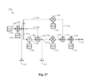
- FIG. 17 is a block diagram of a temperature compensation circuit according to one embodiment.
- FIG. 18A illustrates the relative frequency error residual after a first step of the temperature calibration scheme of FIG. 9 applied to an oscillator using a Lamb wave resonator on a composite silicon dioxide and silicon stack.
- FIG. 18B illustrates the relative frequency error residual after a second step of the temperature calibration scheme of FIG. 9 has been applied to an oscillator using a Lamb wave resonator on a composite silicon dioxide and silicon stack.
- FIG. 18C illustrates the relative frequency error residual after a third step of the temperature calibration scheme of FIG. 9 has been applied to an oscillator using a Lamb wave resonator on a composite silicon dioxide and silicon stack.
- FIG. 19 is a block diagram of a temperature compensation circuit with additional sub-zero correction compared to the embodiment of FIG. 17 , according to another embodiment.
- FIG. 20 illustrates the relative frequency error residual after a fourth step of the temperature calibration scheme of FIG. 9 with additional sub-zero correction applied to an oscillator using a Lamb wave resonator on a composite silicon dioxide and silicon stack, according to another embodiment.
- calibration of oscillator temperature compensation circuitry involves setting values of independently programmable components of the temperature compensation circuitry to cause a desired oscillator frequency response at each of only a small number of discrete temperatures (e.g., less than ten, less than five, etc., but at least three). Accurate temperature compensation over the entire operating temperature range of the oscillator may still be provided, without the need to perform a temperature sweep or any confirmation temperature measurements.
- oscillator temperature compensation circuitry includes at least three independently controllable/programmable components each configured to set the frequency response of the oscillator at a respective temperature. Setting each of the components suitably to provide a desired oscillator frequency response at a respective temperature may provide accurate temperature compensation of the oscillator over the entire operating temperature range (e.g., from ⁇ 40° C. to +85° C. or any other suitable operating temperature range).
- the controllable/programmable components are digital-to-analog converters (DACs).
- FIG. 1 A basic oscillator using a mechanical resonator is shown in FIG. 1 . It comprises a closed loop comprising a resonator 102 producing an output signal 104 and an amplifier 106 producing a feedback signal 108 .
- a closed loop comprising a resonator 102 producing an output signal 104 and an amplifier 106 producing a feedback signal 108 .
- the loop gain equal unity and the phase around the loop is an integer multiple of 360°, including 0°, and negative integers.
- the amplifier will have a phase delay equivalent to 0° phase shift and the mechanical resonator will show a phase shift of 0° at the resonance frequency of the mechanical resonator.
- the oscillator will oscillate at the resonance frequency defined by the resonance frequency of the resonator.
- an inverting amplifier is used that introduces a phase change of ⁇ 180°.
- a phase shift of ⁇ 180° or any odd multiple of 180° has to be added to the oscillator loop for the oscillator to oscillate at a frequency close to or identical to the resonance frequency of the resonator.
- phase shift introduced by the amplifier will range between 0° and as much as ⁇ 45°.
- the resonator might operate at a frequency related to a phase shift that will be close to 0°, but might be as much as ⁇ 45°.
- the applicability of the various aspects described herein is not limited by the amount of phase delay introduced by any of the components of the oscillator.
- the resonance frequency of oscillators including mechanical resonators is temperature dependent.
- the resonance frequency of the mechanical resonator defines the oscillation frequency of the oscillator.
- the resonance frequency of any mechanical resonator is a function of the operating temperature, and in particular the temperature dependence of the stiffness coefficients, density, thermal expansion and temperature related induced stresses of components of the mechanical resonator.
- quartz crystals have been used conventionally as the resonators of choice in oscillators.
- the relative frequency deviation of the resonance frequency for a conventional AT-cut quartz crystal resonator is shown in FIG. 2 .
- the relative frequency deviation over the entire temperature range illustrated is in this case less than ⁇ 8 ppm.
- an oscillator may additionally contribute to temperature-dependent frequency behavior, it can be assumed in appropriate circumstances that the dominant temperature-dependent frequency behavior of an oscillator arises from the mechanical resonator.
- an oscillator including the mechanical resonator operating as shown in FIG. 2 will show substantially the same temperature-dependent behavior.
- FIG. 2 assumes a particular cut angle for the AT-cut quartz crystal. However, altering the cut angle of the quartz crystal alters the temperature dependent behavior of the crystal, and thus the temperature dependent frequency behavior of an oscillator including the quartz crystal.
- FIG. 3 illustrates alternative frequency response curves 304 and 306 of a conventional quartz resonator for two additional cut angles of the quartz crystal.
- the temperature stability of oscillators using quartz AT-cut resonators is generally in the range of ⁇ 10 ppm over a temperature operating range from ⁇ 40° C. to +85° C. For many applications this frequency stability is not sufficient. Numerous applications require frequency stabilities better than ⁇ 2.5 ppm or even ⁇ 0.5 ppm.
- a temperature compensation circuit is added to the oscillator circuit.
- a block diagram of such a device 400 is shown in FIG. 4 .
- the temperature compensation circuit 404 receives signal 410 and employs a tuning method that either induces a frequency shift of the resonator or of the circuit, or both. It should be understood that many techniques are feasible. For the compensation circuit 404 to apply a suitable temperature dependent compensating signal 412 it requires information of the exact temperature of the resonator, which it receives from the connected temperature sensor 406 .
- the achievable temperature accuracy of the temperature compensated oscillator shown in FIG. 4 depends on how deviations of the mechanical resonator, the temperature sensor, the compensation circuit, the circuit components of the oscillator, parasitics, and effects regarding the tuning method employed by the compensation circuitry can be controlled or accounted for by the compensation circuit.
- the compensation circuit comprises different adjustable parameters to account for these variations.
- the actual adjustment of the compensation circuit is performed during a calibration sequence. This assumes though that all contributions are stable with time, i.e. that there is no aging or hysteresis. In reality, there may be variations over time, but that is a separate issue addressed separately from initial calibration of the temperature compensation circuitry.
- plot 550 of FIG. 5B separates the frequency response 502 of FIG. 5A into the various contributions, including first order 552 , second order 554 and third order 556 dependencies. These different temperature dependencies can be related to the temperature dependencies of the resonator material, the electrode materials, stress effects, mounting, and the circuit components of the oscillator. As seen, the linear component 552 is large, as well as the third order component 556 . It is difficult for a circuit to reproduce these different contributions and the resulting characteristics of the frequency response 502 .
- FIG. 6A A conventional circuit 600 used as a temperature compensation circuit for AT-cut quartz resonators is shown in FIG. 6A . It assumes a supply voltage to be applied at the input 602 and the output signal 604 , representing a tuning signal, is shown in FIG. 6B (as 652 in plot 650 ). In this case the compensation circuit is not connected to one temperature sensor, but rather uses three temperature dependent resistors ( 606 , 608 , 610 ), also referred to as thermistors. The resistors 607 , 609 and 611 are adjusted to compensate the temperature characteristics of AT-cut crystals.
- the drawbacks of this technology are that the resistors have to be trimmed and that the output signal is a function of all resistors to be trimmed, i.e., they do not operate independently. That means, although resistor 607 mainly influences the temperature characteristics at very low temperatures it does affect the characteristics at room temperature and high temperatures.
- the resistor 609 is mainly for adjusting the characteristics at room temperature, but nevertheless influences the tuning signal significantly at high temperatures. This means that, after extracting the relative frequency error over temperature for a particular resonator, a sophisticated algorithm is required to compute a set of resistor values ( 607 , 609 , 611 ) for the particular resonator. It also means that errors due to the limited accuracy of the trimming will affect the temperature compensation behavior over the entire temperature range, and as a result the oscillator has to be re-measured to verify the compensation circuit settings.
- the contributions 702 , 704 and 706 are not exclusive for a particular temperature range.
- the tuning signal contains a large contribution from 702 , a significant contribution from 704 and a minor contribution from 706 .
- adjusting contribution 704 will have a significant effect on the tuning signal over the entire temperature range.
- the three contributions cannot be adjusted individually, but instead that all three contributions have to be adjusted as part of an optimizing algorithm after the relative frequency error of the oscillator is known over temperature.
- the calibration procedure for TCXOs with quartz crystal resonators involves multiple temperature sweeps over the entire operating temperature range.
- the process 800 is shown in FIG. 8 .
- the oscillator fabrication process 802 starts at step 804 with the definitions of the oscillator frequency, e.g., 26 MHz, and definition of the tolerances, including the initial frequency accuracy of e.g. ⁇ 1.5 ppm, temperature range, e.g., from ⁇ 40° C. to +85° C. and corresponding temperature stability of the frequency of ⁇ 2.5 ppm.
- the quartz crystal resonator is then fabricated 806 and undergoes a trimming process 850 so that the frequency of the oscillator matches the target frequency of, in this case, 26 MHz with very high accuracy.
- the trimming sequence consists of the actual trimming step 808 , in which material is removed or added to the resonator and a comparison step 810 , in which the obtained oscillator frequency is compared to the desired frequency, which might include some specified offset. If the comparison of these two frequencies is acceptable, the process continues, otherwise the trimming step 808 is repeated and the trimming sequence iterated until the part passes or is classified a faulty part.
- step 812 the oscillator is swept over temperature to evaluate the temperature characteristics. This involves setting the oscillator to a large number (typically around 1,200) of precise temperatures over the anticipated operating temperature range and measuring the oscillator output frequency at each of these temperatures. Then in step 814 , based on the extracted relative frequency error over temperature of the oscillator the temperature compensation circuit is adjusted for that particular oscillator. To verify that the oscillator fulfills the specifications of e.g. ⁇ 2.5 ppm over the entire temperature range the oscillator is then measured over the temperature range once more in step 816 . Step 818 is required to ensure that the adjusted oscillator meets the specifications. If the oscillator passes this stage it is complete ( 820 ). If it does not pass, the part might be re-adjusted (step 814 ) and the measurement procedure 816 repeated or the part classified as faulty.
- each oscillator behaves differently so that each oscillator has to be measured over the entire temperature range and adjusted individually.
- the temperature measurements require a very high accuracy on the temperature control during the measurement. As a result, the temperature slope for the measurement is very low and the measurement procedure takes a lot of time. Because the temperature sweep is performed twice (i.e., steps 812 and 816 ), the time is even greater.
- a procedure for calibrating temperature compensated oscillators including TCXOs, is provided that is much faster than conventional methods, and only requires the measurement of the oscillator frequency at a small number of temperatures, as few as two, three or four temperatures.
- compensation circuits are provided for performing the method just described, and include independently controllable components for calibrating the compensation circuit at respective temperatures.
- FIG. 9 A non-limiting example of a procedure for calibrating oscillators having mechanical resonators according to an aspect of the technology is shown in FIG. 9 .
- the oscillator fabrication process 902 starts with the definitions of the oscillator frequency, e.g., 125 MHz, and definition of the tolerances, including the initial frequency accuracy of e.g., ⁇ 2.5 ppm, temperature range, e.g., from ⁇ 40° C. to +85° C. and corresponding temperature stability of the frequency of ⁇ 2.5 ppm. Additional specifications are possible.
- the resonator is then fabricated 906 .
- arbitrary frequency refers to a frequency not substantially matching a conventional standard oscillator frequency.
- the arbitrary frequency may differ by at least 30 parts per million (ppm) from a standard oscillator frequency in some embodiments.
- the arbitrary frequency may differ by at least 50 ppm from a standard oscillator frequency, by at least 100 ppm, by at least 200 ppm, by at least 500 ppm, by at least 1,000 ppm, or by between approximately 1,000 ppm and 10,000 ppm (e.g., 2,000 ppm, 5,000 ppm, or any other value within this range), among other possible amounts of deviation.
- the term “arbitrary frequency” as used herein does not imply the frequency is not known or cannot be measured. Rather, an arbitrary frequency may be measured or otherwise have its value determined
- the oscillator frequency is measured at a first temperature (step 908 ), e.g., around room temperature with a rather large tolerance on the temperature accuracy, and the frequency of the oscillator recorded at 910 within, for example, memory of the oscillator or a test-computer.
- the step 950 may be omitted since the initial frequency value can be arbitrary, so that step 920 may be performed directly after step 906 .
- the illustrated step 950 may be replaced with a trimming step of the type previously described with respect to step 850 .
- step 920 the oscillator is exposed to a well-defined first temperature (Temperature 1 ), which is controlled within an accuracy of ⁇ 5 K, ⁇ 1 K, ⁇ 0.5 K or even ⁇ 0.1 K, as non-limiting examples. Larger values are also possible.
- the oscillator frequency is then measured.
- the compensation circuit within the oscillator is then adjusted (step 922 ) and the resulting (adjusted) oscillator frequency is compared to the desired frequency in step 924 .
- the procedure of measuring 920 , adjusting 922 and comparing 924 is repeated until the oscillator frequency matches the desired frequency at the first temperature.
- the desired frequency may be any suitable value, and that the method illustrated in FIG. 9 is not limited in this respect.
- the desired frequency may be the frequency determined and stored in step 910 , or it may be the frequency measured in step 920 . In such situations, no circuit adjustment may be necessary at 922 .
- the desired frequency may be computed based on the stored frequency in 910 and the measured frequency of step 920 .
- the frequency used for comparison in step 924 may be the frequency determined and stored in step 910 including a defined offset, may be the frequency measured in step 920 with a specified offset, or may be a frequency computed based on the stored frequency in 910 and the measured frequency of step 920 including an offset, among other possibilities.
- step 930 the oscillator is exposed to a well-defined second temperature (Temperature 2 ), which is controlled within an accuracy of ⁇ 5 K, ⁇ 1 K, ⁇ 0.5 K or even ⁇ 0.1 K, as non-limiting examples. Larger values are also possible.
- the oscillator frequency is then measured.
- the compensation circuit within the oscillator is then adjusted (step 932 ) and the resulting (adjusted) frequency is compared to the desired frequency in step 934 .
- the procedure of measuring 930 , adjusting 932 and comparing 934 is repeated until the oscillator frequency matches the desired frequency.
- the desired frequency used for comparison in 934 is the same as the frequency used for the comparison in 924 .
- the desired frequency in 934 may be chosen to include an offset to the desired frequency used in 924 .
- step 940 the oscillator is exposed to a well-defined third temperature (Temperature 3 ), which is controlled within an accuracy of ⁇ 5 K, ⁇ 1 K, ⁇ 0.5 K or even ⁇ 0.1 K, as non-limiting examples. Larger values are also possible.
- the oscillator frequency is then measured.
- the compensation circuit within the oscillator is then adjusted 942 and the resulting (adjusted) frequency is compared to the desired frequency in step 944 .
- the procedure of measuring 940 , adjusting 942 and comparing 944 is repeated until the oscillator frequency matches the desired frequency (in which case the procedure is completed at 946 ).
- the desired frequency used for comparison in 944 is the same as the frequency used for the comparison in 924 and 934 .
- the desired frequency in 944 may be chosen to comprise an offset to the desired frequency used in 934 .
- step 944 If the oscillator has passed step 944 , it is complete. If the oscillator repeatedly does not pass the comparison steps 924 , 934 , or 944 or if the frequency despite the adjustment is not able to approach the comparison frequency, the part is classified as faulty and taken out of the procedure. It should be further appreciated that the embodiment shown in FIG. 9 containing three temperature points and circuit adjustment steps can be extended to comprise additional temperatures and circuit adjustment steps, and can contain four, five or even six such calibration steps and is not limited in this respect. The greater the number of temperatures measured, the greater the accuracy of the calibration.
- the method illustrated in FIG. 9 may be used beneficially for oscillators including various types of mechanical resonators.
- the method may be used beneficially for oscillators having microelectromechanical systems (MEMS) resonators.
- MEMS microelectromechanical systems
- the method may also be used beneficially for oscillators using quartz resonators, thus avoiding the temperature sweeps associated with the conventional method of FIG. 8 for calibrating such oscillators.
- FIG. 10 One embodiment of a temperature compensation circuit which may utilize the calibration procedure 900 is shown in block diagram form in FIG. 10 . It comprises a temperature sensor 1002 that outputs a current, voltage or charge dependent on the temperature. Initially, the digital to analog converters 1024 , 1028 , 1032 are all set to their smallest value, i.e., zero.
- the calibration of circuit 1000 of FIG. 10 may depend on the type of resonator being used with the oscillator of which the circuit 1000 is a part. If an AT-cut crystal is used that is trimmed to a specific frequency the sequence 950 may be replaced with the trimming procedure 850 . For an arbitrary frequency oscillator, sequence 950 may be used or omitted depending on whether a circuit adjustment is necessary at the first step or not, as discussed above. In explaining the calibration of circuit 1000 , we will assume that the procedure 950 is omitted.
- the circuit is initially set to a desired first temperature at step 920 , for example by adjusting the circuit temperature until the temperature sensor 1002 indicates the circuit is at the desired temperature.
- the circuit temperature may be adjusted until the output of the temperature sensor 1002 is nulled.
- the frequency of the oscillator is then measured at step 920 .
- This first temperature step can be chosen arbitrarily, but a temperature close to the center of the expected operating temperature range of the oscillator is advantageous. Room temperature (25° C.) is a preferred temperature, however, other temperatures are also possible.
- the electrical signal at 1010 is measured by measuring the electrical signal at Pin A 1012 .
- the electrical signal 1010 is the sum of the temperature sensor signal 1004 and a value stored in element 1006 (a digital-to-analog converter (DAC) in this non-limiting embodiment) formed by the adder 1008 .
- the objective is to null the signal 1010 .
- DAC 1006 digital-to-analog converter
- the signal 1010 is set to zero.
- a special pin e.g., pin 1012
- signal 1010 may be provided at the oscillator output.
- the measurement of 1010 might occur internally and a value relating to the level of signal 1010 might be accessible through memory in the oscillator that is also accessible from the outside.
- the signal 1010 is zero at the first temperature.
- the signals 1014 a , 1014 b and 1014 c are also zero. Therefore, the output signal of the adder 1016 is also zero.
- the tuning circuit output signal 1022 from adder 1020 is therefore determined by the value stored in 1018 (also a DAC in this non-limiting embodiment).
- This value can be either left as is, corresponding to the case where the desired frequency is chosen as the frequency measured in step 920 and therefore no adjustment is necessary or the value is adjusted to match a desired frequency based on the oscillator specifications from step 904 , the frequency stored in step 910 , or the value measured in step 920 , or a combination of the former three, including any arbitrary offset.
- the value of DAC 1018 can also be chosen to match a certain number of significant digits, e.g., if the measured frequency in step 920 is, e.g., 124,897,064.26 Hz the desired frequency could be chosen to require fewer significant digits, e.g., 124,897,000.00 Hz. No matter how it is chosen, this first frequency that is used for the adjustment criteria is referred to as the desired frequency.
- the linear coefficient of the temperature characteristics of the oscillator is adjusted.
- the oscillator is brought to the second temperature, step 930 , and the frequency of the oscillator measured.
- the linear term of the compensation signal which is produced by mixer 1026 (M 1 ) and is controlled by DAC 1024 , is then adjusted at step 932 by programming 1024 so that the oscillator output (not shown in FIG. 10 ) is equal to the desired frequency or offset from the desired frequency by a specific amount, i.e., until the result passes at comparison step 934 .
- the oscillator is now compensated to first order.
- the typical temperature dependent frequency response 202 of an AT-cut quartz crystal is shown in plot 200 of FIG. 2 before linear compensation.
- the temperature dependent frequency response 1102 after the linear compensation just described is shown in plot 1100 of FIG. 11A .
- the point indicated by 1104 represents the working point (at a temperature represented by the corresponding vertical line) where the frequency error is minimized by adjusting the circuit as just described.
- the vertical gray lines represent temperatures which may be used in the calibration processes (e.g., Temperature 1 , Temperature 2 , Temperature 3 , etc.).
- the frequency response of the AT-cut crystal also comprises large second and third order components.
- a temperature is chosen where the second and third order coefficients are equal in amplitude, but opposite in sign.
- this temperature is between 34° C. and 39° C. Thus, this temperature range is preferred for adjusting the linear coefficient.
- the quadratic temperature dependence is adjusted.
- Element 1028 (a DAC in this non-limiting example) is adjusted to yield a quadratic term 1030 that is added by adder 1016 to the already adjusted linear signal 1014 a .
- a third temperature is chosen that lies either in between the first and second temperatures or that lies below the first temperature but within some range of the first temperature, the range being defined by the difference of the first temperature minus the second temperature.
- Other temperatures for the third temperature are also possible, especially if the resonator is not an AT-cut crystal.
- the oscillator After adjusting the circuit for the third temperature to match the desired frequency, possibly including an offset, the oscillator passes the comparison 944 and the resulting temperature dependent frequency response including a first and second order compensation is shown in FIG. 11B .
- the point indicated by 1114 represents the working point where the frequency error is minimized by adjusting the circuit, and the vertical gray lines represent the temperatures used during the calibration process.
- the frequency response 1112 still contains a large third order contribution, which may be removed with a measurement at another temperature in addition to those illustrated in FIG. 9 (i.e., at a “Temperature 4 ” after the processing at “Temperature 3 ”). While this additional processing at yet another temperature is not illustrated in FIG. 9 for purposes of simplicity of the illustration, it should be understood that the processing at this additional temperature is identical to the processing performed at the first, second and third temperatures (i.e., Temperatures 1 - 3 ), meaning that the processing involves measuring the oscillator frequency at Temperature 4 and then adjusting the circuit to provide the desired frequency response at that temperature, and repeating as necessary.
- the cubic component 1034 in FIG. 10 is adjusted using the DAC 1032 until the desired frequency is reached, possibly including an offset. After passing this comparison the part is completed.
- the frequency response of the fully adjusted oscillator is shown in plot 1120 of FIG. 11C .
- the point indicated by 1124 represents the working point where the frequency error is minimized by adjusting the circuit as just described. As shown, the frequency error of 1112 is well below the typical temperature stability of AT-cut crystal based oscillators.
- the temperature dependent frequency response of a crystal oscillator may depend on the cut angle of the oscillator.
- Applying the calibration procedure just described to AT-cut crystal-based oscillators for the three different cut angles used to generate the frequency response curves of plot 300 in FIG. 3 results in the three corresponding curves shown in plot 1200 of FIG. 12 , where 1202 corresponds to the initial curve 202 after compensation using the method of FIG. 9 , 1204 corresponds to 304 after compensation, and 1206 corresponds to 306 after compensation.
- 1202 corresponds to the initial curve 202 after compensation using the method of FIG. 9
- 1204 corresponds to 304 after compensation
- 1206 corresponds to 306 after compensation.
- the temperature error is very small for the temperature range spanned by the smallest and largest measurement temperature. However, for temperatures outside of the temperature range spanned by the calibration temperatures the error is considerable. In this example negative temperatures have been avoided, i.e.
- the smallest temperature in this example is 22.5° C.
- several methods can be used. One method expands the temperature test range to include negative temperatures. Another method is based on using a known offset for the frequency adjustment to account for the negative temperatures. Another method uses an offset added or subtracted to the temperature sensor.
- plot 1300 of FIG. 13A illustrates an alternative shape of a temperature dependent frequency response of an oscillator, shown by the line 1302 .
- a frequency response like that shown in FIG. 13A may be exhibited by the types of resonators having a temperature compensated stack comprising layers of silicon dioxide, silicon, and silicon dioxide, as described in U.S. patent application Ser. No. 12/639,161, filed on Dec.
- the turnover temperature i.e., the temperature at which the frequency response hits a peak value, like that shown in FIG. 13A
- the turnover temperature is designed to lie close to the center of the temperature operating range.
- silicon has a large negative first order coefficient of frequency, a large second order contribution and a significant third order contribution, related to the stiffness dependence over temperature and thermal expansion dependence over temperature.
- Silicon dioxide possesses the rare characteristic that the stiffness increases with increasing temperature.
- This rare characteristic can be used to create temperature stable resonators by matching the silicon dioxide thickness to the silicon thickness.
- the first order temperature dependence can be accounted for, as shown in FIG. 13A .
- a large second order dependence remains as seen from FIG. 13A , that also includes a significant third order contribution that is hard to make out from trace 1302 .
- the cut angle dependence of the crystal resonator is one of the biggest factors that influences the resulting temperature characteristics, as shown in FIG. 3 .
- a composite compensating layer stack e.g., a composite stack including silicon sandwiched between layers of silicon dioxide, as described in the above-incorporated U.S. patent application Ser. No. 12/639,161
- the temperature characteristics are influenced by the thickness tolerances in manufacturing the composite stack.
- the effect of the thickness variations for a compensated stack resonator are shown in FIG. 13B .
- the calibration procedure described herein is versatile enough to account for these variations of the temperature characteristics originating from the thickness variations.
- FIGS. 14A-C The results of applying the calibration procedure shown in FIG. 9 to a compensated stack resonator having the pre-calibration frequency response shown in FIG. 13A (e.g., of the type described in the above-incorporated U.S. patent application Ser. No. 12/639,161) are shown in FIGS. 14A-C .
- the sequence 950 may be used or omitted depending on whether a circuit adjustment is necessary at the first step or not, as discussed above. We will assume here that the procedure 950 is omitted.
- the circuit is initially set to a desired first temperature at step 920 , for example by adjusting the circuit temperature until the temperature sensor 1002 indicates the circuit is at the desired temperature.
- the circuit temperature may be adjusted until the output of the temperature sensor 1002 is nulled.
- the frequency of the oscillator is then measured at step 920 .
- This first temperature step can be chosen arbitrarily, but a temperature close to the center of the expected operating temperature range of the oscillator is advantageous. Room temperature (25° C.) is a preferred temperature, however, other temperatures are also possible.
- the electrical signal at 1010 is measured by measuring the electrical signal at Pin A 1012 .
- the electrical signal 1010 is the sum of the temperature sensor signal 1004 and a value stored in element 1006 (a DAC in this non-limiting embodiment) formed by the adder 1008 .
- the objective is to null the signal 1010 .
- the signal 1010 is set to zero.
- a special pin e.g., pin 2010
- signal 1010 may be provided at the oscillator output.
- the measurement of 1010 might occur internally and a value relating to the level of signal 1010 might be accessible through memory in the oscillator that is also accessible from the outside.
- the signal 1010 is zero at the first temperature.
- the signals 1014 a , 1014 b and 1014 c are also zero. Therefore, the output signal of the adder 1016 is also zero.
- the tuning circuit output signal 1022 is therefore determined by the value stored in 1018 . This value can be either left as is, corresponding to the case where the desired frequency is chosen as the frequency measured in step 920 and therefore no adjustment is necessary or the value is adjusted to match a desired frequency based on the oscillator specifications from step 904 , the frequency stored in step 910 , or the value measured in step 920 , or a combination of the former three, including any arbitrary offset.
- the value of DAC 1018 can also be chosen to match a certain number of significant digits, e.g., if the measured frequency in step 920 is e.g., 124,897,064.26 Hz the desired frequency could be chosen to require fewer significant digits, e.g., 124,897,000.00 Hz. No matter how it is chosen, this first frequency that is used for the adjustment criteria is referred to as the desired frequency.
- the linear coefficient of the temperature characteristics of the oscillator is adjusted.
- the oscillator is brought to the second temperature, step 930 , and the frequency of the oscillator measured.
- the linear term of the compensation signal which is produced by mixer 1026 (M 1 ) and is controlled by DAC 1024 is then adjusted at step 932 by programming 1024 so that the oscillator output (not shown in FIG. 10 ) is equal to the desired frequency or offset from the desired frequency by a specific amount, i.e., until the result passes at comparison step 934 .
- the oscillator is now compensated to first order.
- the typical temperature dependent frequency response of stack compensated resonators before compensation, 1302 , 1354 and 1356 are shown in plot 1350 of FIG. 13B .
- plot 1400 of FIG. 14A After this first compensation step the results shown in plot 1400 of FIG. 14A are obtained, where it is hard to separate the different traces from each other, as indicated by 1402 .
- the point indicated by 1404 represents the working point where the frequency error is minimized by adjusting the circuit as just described.
- the second temperature is chosen very close to the center of the temperature range or the first temperature. This decision is based on the temperature characteristics of the resonator. We had seen that for AT-cut crystals it is advantageous to use a temperature between 34° C. and 39° C. for the extraction of the linear coefficient. For a resonator that is dominated by linear and quadratic components, as is the case for almost all non-quartz mechanical resonators, the temperature used for the linear adjustment is chosen close to the center of the temperature range, i.e. within ⁇ 10K, ⁇ 20K, although other values are also possible.
- the quadratic temperature dependence is adjusted.
- Element 1028 is adjusted to yield a quadratic term 1030 that is added by adder 1016 to the already adjusted linear signal 1014 a .
- the third temperature is chosen to lie at one extreme of the temperature range. As positive temperatures are technically easier to obtain the maximum temperature of +85° C. is used in this case.
- the oscillator passes comparison 944 and the resulting temperature characteristics including first and second order compensation are shown in FIG. 14B .
- the point indicated by 1418 represents the working point where the frequency error is minimized by adjusting the circuit as just described.
- a fourth temperature may be used to reduce the effect of the third order contribution.
- a fourth temperature i.e., a “Temperature 4 ” not illustrated in FIG. 9 but being used after “Temperature 3 ” in FIG. 9
- the reduction of the third order dependence is only marginal, as seen from plot 1420 of FIG. 14C , in which 1424 corresponds to 1414 of FIG. 14B , 1426 corresponds to 1416 of FIG. 14B , and 1422 corresponds to 1412 of FIG. 14B .
- the fourth temperature is chosen in between the second and third temperatures the characteristics for positive temperatures are improved at the cost of the frequency error for negative temperatures. Therefore, a modification to the calibration sequence may be made to provide even greater reduction of the frequency error.
- the modified sequence uses an adjustment step at a first temperature to null the temperature sensor, as previously described (e.g., by adjusting the circuit temperature until the temperature sensor output is nulled).
- the next adjustment step at the second temperature is used to compensate the linear contribution as before, leading to the result shown in plot 1500 of FIG. 15A , which is identical to the frequency response shown in FIG. 14A (i.e., 1502 is identical to 1402 and 1504 is identical to 1404 , although it should be noted that FIGS. 14A and 15A differ in that the graphs illustrate not only the frequency response but also the temperatures (shown in the vertical gray lines) at which the calibration steps are performed, and FIG. 15A shows a temperature at 15 Kelvin whereas FIG.
- 14A shows the corresponding temperature line at between 55 and 60 Kelvin).
- the second order contribution is adjusted and the result is shown in plot 1510 of FIG. 15B , which illustrates an identical frequency response to that of FIG. 14B (i.e., 1512 is identical to 1412 , 1514 is identical to 1414 , 1516 is identical to 1416 , and 1518 is identical to 1418 ), although again the figures differ in that the illustrated test temperatures (shown by the vertical gray lines) differ.
- the fourth temperature which is chosen to lie in between the second and third temperatures, the linear term controlled by 1024 is re-adjusted.
- the process may involve re-adjusting the DAC 1024 to ensure that the linear term is compensated by readjusting the DAC value until the oscillator frequency at the fourth temperature matches the desired frequency.
- This readjustment at the fourth temperature results in the traces 1602 , 1604 and 1606 in plot 1600 of FIG. 16A , where 1608 represent the working point at the fourth temperature.
- Compensation of the third order contribution may then be performed using a fifth temperature, which can be chosen to be identical with the third temperature, resulting in the behavior illustrated in plot 1610 of FIG. 16B .
- Trace 1614 corresponds to 1604 of FIG. 16A after using the fifth temperature 1618 .
- traces 1612 and 1616 correspond to traces 1602 and 1606 , respectively, after compensation at the fifth temperature.
- the third order contribution may be removed.
- the residual frequency error after passing this calibration sequence is about ⁇ 1 ppm, and even smaller in the temperature range spanned by the smallest and largest temperature used during the calibration (see FIG. 16B ). To reduce the residual error even more, negative temperatures can be used during the calibration.
- the first is that a first temperature step is required to null the temperature sensor reading. As a result, adjustment of the circuit at four to five temperatures is necessary to obtain a third order compensation of the circuit.
- adjusting the circuit components as described at any given temperature affects not only the frequency response at that temperature but also at other temperatures, including previously tested temperatures. This effect becomes more severe if non-ideal behavior of the circuit components is included, such that the frequency measurement may be limited to an accuracy of, e.g., 0.1 ppm.
- circuit block diagram 1700 shown in FIG. 17 addresses the characteristics of circuit 1000 just described since they may be undesirable in some situations.
- the circuit 1700 includes a temperature sensor 1702 producing a temperature sensor signal 1704 , which is provided to adder A 1 1708 .
- DAC* 1 1706 also provides its output signal to adder 1708 .
- the adder 1708 outputs signal 1710 , which may be measured at Pin A 1712 .
- the output signal 1710 is branched into signals 1710 a , 1710 b , and 1710 c , which are provided to mixer M 1 1734 , adder A 2 1730 , and quadratic component 1726 , respectively.
- DAC 3 1724 also provides its output to the quadratic component 1726 , which produces signal 1728 .
- Adder A 2 1730 produces an output signal 1732 a which may be measured at Pin B 1732 and which is provided to mixer M 2 1738 .
- DAC 5 1736 also provides its output signal to mixer 1738 , the output 1714 b of which is provided to adder 1716 .
- Adder 1716 also receives an output signal 1714 a of mixer M 1 1734 .
- mixer 1734 receives 1710 a as one input and also receives the output of DAC 4 1732 as a second input.
- Adder 1716 is coupled to adder A 4 1720 to provide its output signal to adder 1720 .
- DAC* 2 1718 also provides it output to adder 1720 , which then provides output 1722 of the circuit.
- the circuit 1700 does not require a distinct calibration of the temperature sensor signal 1704 from temperature sensor 1702 , and the frequency error at a given temperature is not affected by subsequent adjustments.
- including the sequence of 950 in method 900 is of interest as it can help during the first actual tuning step to estimate what the overall frequency error over temperature is for a specific oscillator. From knowing the frequency of the oscillator around, e.g., room temperature and at the first measurement temperature Temperature 1 (step 920 ) the overall temperature characteristic can be estimated. This is understood from examining FIG. 13B around room temperature and the frequency deviation for a 60K higher temperature. Even if the temperature accuracy of the initial frequency measurement in step 908 is large, as large as ⁇ 5° C., ⁇ 10° C.
- the temperature characteristics can be estimated. From this estimate, the required tuning range can be determined and used to define the desired frequency of the oscillator. In general, tuning an oscillator will cause the phase noise of the oscillator to increase, which is undesirable. From being able to estimate the required tuning range, the desired frequency can be chosen to fulfill various possible requirements of interest. For example, if an optimum of the phase noise is desired around a specific temperature, the desired frequency can be chosen to coincide with the frequency the oscillator would have at this temperature with a tuning signal of zero. In another case, better phase noise performance may be desired for positive temperatures than at negative temperatures, which may be achieved by choosing the desired frequency to coincide with the frequency of the oscillator with the tuning signal being zero for a temperature larger than the center of the temperature range.
- the oscillator is exposed to a first well controlled temperature as part of step 920 .
- this first temperature is chosen at one of the extremes of the temperature range. A positive temperature is generally more desirable.
- the temperature signal 1710 (output by adder 1708 ) is adjusted to zero by controlling DAC 1706 to cancel the temperature sensor signal 1704 , which is done by measuring the electrical signal at Pin A 1712 .
- the tuning signal 1722 depends on the value stored in DAC 1718 .
- the oscillator frequency is measured and adjusted to match the desired frequency by adjusting the value stored in 1718 .
- the resulting temperature characteristics are shown in plot 1800 of FIG. 18A , which correspond to the results of FIG. 13B simply shifted to be zero at the point indicated by 1808 (i.e., 1802 is a shifted version of 1302 , 1804 is a shifted version of 1354 , and 1806 is a shifted version of 1356 ).
- the oscillator is then exposed to the second temperature and the frequency measured in step 930 .
- This temperature is chosen closer to the most negative extreme of the temperature range. In some cases it might be desirable to use a temperature around 0° C. or +5° C., or above ⁇ 20° C. to avoid technical difficulties of the temperature control and icing related reliability issues.
- the circuit is then adjusted at step 932 by measuring the electrical signal 1732 a at Pin B 1732 and adjusting DAC 1724 until the electrical signal 1732 a is zero. Then DAC 4 1732 is adjusted until the oscillator frequency matches the desired frequency.
- the resulting frequency error over temperature is shown in plot 1810 of FIG. 18B , in which 1812 represents the frequency error and 1814 represents the working point of the second temperature.
- a temperature in between the first and second temperatures is chosen.
- the value of DAC 1736 is adjusted until the oscillator frequency matches the desired frequency.
- the resulting frequency error is shown in plot 1820 of FIG. 18C , with traces 1822 , 1824 , and 1826 .
- Point 1828 represents the working point at the third temperature. It should be appreciated that for all traces 1822 , 1824 and 1826 the frequency error at the three measurement temperatures is zero.
- the residual frequency error is mostly below ⁇ 0.5 ppm, however it exceeds this range for the negative temperature range.
- Circuit 1900 includes additional components such as diode 1940 , DAC 6 1942 , and mixer M 3 1944 .
- the signal 1732 a output by adder A 2 1730 (which may be measured with Pin B 1932 ) is branched to signal 1732 b and provided to the diode 1940 .
- the diode 1940 compares the value of signal 1732 b to zero and passes the signal only if it is greater than zero. Any suitable circuit component for performing such a function may be used, as a diode is a non-limiting example.
- the output of diode 1940 is input to mixer M 3 1944 , which also receives an output of DAC 6 1942 .
- Mixer 1944 then output signal 1714 c to adder 1916 .
- Adder 1916 is similar to adder 1716 of FIG. 17 , except that it receives the additional input 1714 c where adder 1716 does not.
- the output of adder 1916 is provided to adder A 4 1720 , as is the output of DAC* 2 1718 .
- Adder 1720 then provides the output signal 1922 of the circuit.
- Circuit 1900 contains the element DAC 6 1942 that can be adjusted either at a fourth temperature by matching the oscillator frequency to the desired frequency or 1942 might be set to a value based on the values used for 1724 and DAC 4 1732 .
- the non-linearity of the digital to analog converter can have an effect on the accuracy of the tuning signal.
- the result shown in FIG. 18C is improved for negative temperatures, as shown in plot 2000 of FIG. 20 .
- trace 2002 corresponds to trace 1822 of FIG. 18C improved for negative temperature
- trace 2004 corresponds to trace 1824 improved for negative temperatures
- trace 2006 corresponds to trace 1826 improved for negative temperatures. In this case the adjustment was done based on the values used for 1724 and DAC 4 1732 .
- temperatures e.g., the method of FIG. 9
- as few as two temperatures may be used while still providing accurate temperature calibration and compensation.
- temperature measurements and circuit adjustments may be performed at two temperatures (e.g., Temperatures 1 and 2 in FIG. 9 ) as previously described to compensate the linear error.
- Further temperature measurements may not be needed to compensate the second order error because, for example, the second order error may be known or substantially known beforehand (for example, in situations in which the second order error does not vary significantly from resonator to resonator and is therefore known from measurements performed on previous resonators).
- the third order error may simply not be compensated in some situations if not desired.
- accurate temperature compensation may be provided using as few as two temperature points.
- One or more benefits compared to conventional calibration and temperature compensation technology may be realized by utilizing the aspects described herein.
- the time involved in calibrating temperature compensation circuitry may be reduced, and in some instances significantly reduced, by utilizing one or more of the aspects described.
- much less time may be involved in using the methods described herein in which significantly fewer temperatures are analyzed (e.g., ten temperatures or less).
- conventional calibration techniques require a second temperature sweep over the entire operating temperature range, at least some of the aspects described herein may negate the need for any such confirmation temperature sweep, thus saving further time and effort.
- the aspects described herein allow for temperature calibration to be performed without precise temperatures, thus easing constraints on the process.
- the calibration may be performed irrespective of whether the test temperature is, for example, 33C or 35C.
- stable test temperatures may be sufficient (e.g., a test temperature that remains at 33C during the testing at that temperature).
- circuits and methods for calibrating temperature compensation circuitry of an oscillator by measuring the frequency of the oscillator at distinct and well controlled temperatures and adjusting a circuit until the oscillator frequency matches the desired frequency are provided.
- the calibration may be performed without measuring the oscillator behavior over an entire operating temperature range and without computing best adjustment settings for multiple components of a temperature compensation circuit.
- aspects of the present invention may be simpler and more robust than conventional techniques for calibration of temperature compensation circuitry.
- the frequency error for the temperatures used to adjust the calibration circuit may be minimal and may not be affected by any subsequent calibration step.
- the adjustment of individual components of a temperature compensation circuit may be independent of the adjustment of other components of the circuit.
- a calibration method of an oscillator for calibrating the oscillator frequency behavior over a temperature range (e.g., an operating temperature range).
- the calibration may method may be designed to avoid any final temperature sweep conventionally required to ensure accuracy of the calibration.
- the calibration method also, or alternatively, does not require a full sweep over the entire temperature operating range before adjusting the temperature compensation circuit.
- the calibration method involves making circuit adjustments at each of multiple temperature steps of the calibration method, rather than measuring the oscillator frequency at many temperatures and then making one adjustment.
- the calibration method may use temperatures that are precise (stable) (i.e. temperature stability of e.g. ⁇ 2K, ⁇ 0.5K, ⁇ 0.1K) but not necessarily accurate (i.e., that do not necessarily equal a specifically targeted temperature value).
- temperature compensation circuitry including one or more digital-to-analog converters (DACs).
- Calibration of the temperature compensation circuitry may comprise adjusting the DACs by programming them.
- the DACs are non-linear, though in some embodiments linear DACs may be used.
- the temperature calibration may be performed without evaluating the DAC digital-to-analog conversion relation prior to setting the DAC.
- the calibration may involve adjusting each DAC until the oscillator frequency matches a desired frequency.
- compensation of arbitrary frequency oscillators may be accomplished using one or more of the techniques described herein.
- the techniques may be applied to various types of oscillators, and arbitrary frequency oscillators represent a non-limiting example.
- temperature calibration techniques described herein may utilize various temperatures for the calibration.
- Various scenarios are possible, some non-limiting examples of which are now described.
- a temperature between 34° C. and 39° C. may be implemented as a second temperature.
- a temperature between 11° C. and 39° C. (e.g., between 35° C. and 39° C.) may be used as a third temperature.
- a temperature between 39° C. to 85° C. or lower than 11° C. e.g., between 11° C. and ⁇ 40° C.
- a temperature between 39° C. to 85° C. or lower than 11° C. e.g., between 11° C. and ⁇ 40° C.
- a temperature between 39° C. to 85° C. or lower than 11° C. e.g., between 11° C. and ⁇ 40° C.
- a temperature close to the center of the operating temperature range may be chosen as the second temperature, e.g., within the range including the center of the temperature range ⁇ 20% of the absolute range of the temperature range.
- a temperature close to the extremes of the temperature range may be selected as a third temperature, e.g., within 30% tolerance of the absolute range of the temperature range.
- the fourth temperature may be chosen in the center of the third temperature and second temperature within 20% tolerance of the absolute temperature range.
- the fourth temperature may be located within ⁇ 25% from the extreme temperature with a 40% tolerance of the absolute temperature range.
- a temperature close to the extremes of the temperature range may be selected as a fifth calibration temperature, e.g., within 40% of the absolute range of the temperature range.
- the techniques described herein may be applied to calibration of an oscillator when the lowest temperature range of calibration is not lower than the center of the specified operating range of the oscillator.
- the calibration may be applied when the lowest temperature of the calibration is 10% of the total operating temperature range lower than the center temperature of the operating range.
- the calibration may be applied when the lowest temperature of the calibration is 20% of the total operating temperature range lower than the center temperature of the operating range.
- the calibration may be applied when the lowest temperature of the calibration is 30% of the total operating range lower than the center temperature of the operating range. Alternatives are possible.
Landscapes
- Oscillators With Electromechanical Resonators (AREA)
Abstract
Description
Claims (6)
Priority Applications (1)
| Application Number | Priority Date | Filing Date | Title |
|---|---|---|---|
| US13/182,008 US8729976B2 (en) | 2010-07-13 | 2011-07-13 | Methods and apparatus for calibration and temperature compensation of oscillators having mechanical resonators |
Applications Claiming Priority (2)
| Application Number | Priority Date | Filing Date | Title |
|---|---|---|---|
| US36375910P | 2010-07-13 | 2010-07-13 | |
| US13/182,008 US8729976B2 (en) | 2010-07-13 | 2011-07-13 | Methods and apparatus for calibration and temperature compensation of oscillators having mechanical resonators |
Publications (2)
| Publication Number | Publication Date |
|---|---|
| US20120013410A1 US20120013410A1 (en) | 2012-01-19 |
| US8729976B2 true US8729976B2 (en) | 2014-05-20 |
Family
ID=45466495
Family Applications (1)
| Application Number | Title | Priority Date | Filing Date |
|---|---|---|---|
| US13/182,008 Active US8729976B2 (en) | 2010-07-13 | 2011-07-13 | Methods and apparatus for calibration and temperature compensation of oscillators having mechanical resonators |
Country Status (2)
| Country | Link |
|---|---|
| US (1) | US8729976B2 (en) |
| WO (1) | WO2012009429A1 (en) |
Families Citing this family (14)
| Publication number | Priority date | Publication date | Assignee | Title |
|---|---|---|---|---|
| KR100926461B1 (en) * | 2007-12-14 | 2009-11-13 | 한국표준과학연구원 | Method for the Measurement of Store and Dew Point at Low Temperature Using Crystal Microbalance Dew Point Sensor |
| US8476809B2 (en) | 2008-04-29 | 2013-07-02 | Sand 9, Inc. | Microelectromechanical systems (MEMS) resonators and related apparatus and methods |
| US8410868B2 (en) | 2009-06-04 | 2013-04-02 | Sand 9, Inc. | Methods and apparatus for temperature control of devices and mechanical resonating structures |
| US9048811B2 (en) | 2009-03-31 | 2015-06-02 | Sand 9, Inc. | Integration of piezoelectric materials with substrates |
| US8884718B2 (en) * | 2011-08-09 | 2014-11-11 | Si-Ware Systems | Method and apparatus to control the LC tank temperature null characteristic in a highly stable LC oscillator |
| US9185659B2 (en) | 2012-10-25 | 2015-11-10 | Qualcomm Incorporated | Two-dimensional transmit power compensation |
| FR3005223B1 (en) | 2013-04-30 | 2015-04-24 | Sagem Defense Securite | METHOD FOR CONTROLLING A PIEZOELECTRIC DEVICE WITH PIEZOELECTRIC ELEMENT REPORTED ON A SUPPORT |
| JP5923648B1 (en) * | 2015-07-10 | 2016-05-24 | レノボ・シンガポール・プライベート・リミテッド | Input device and electronic device |
| FI128032B (en) | 2017-09-05 | 2019-08-15 | Tikitin Oy | Oven-controlled frequency reference oscillator and method of fabricating thereof |
| US10425084B2 (en) * | 2017-10-03 | 2019-09-24 | Murata Manufacturing Co., Ltd. | Oven controlled MEMS oscillator and system and method for calibrating the same |
| CN110212911B (en) * | 2019-06-24 | 2023-04-07 | Oppo广东移动通信有限公司 | Frequency calibration method and device and storage medium |
| US11283403B1 (en) * | 2020-12-23 | 2022-03-22 | Txc Corporation | Temperature-controlled and temperature-compensated oscillating device and method thereof |
| US11514990B1 (en) * | 2021-06-17 | 2022-11-29 | Sandisk Technologies Llc | Two way single VREF trim for fully differential CDAC for accurate temperature sensing |
| CN116880430B (en) * | 2023-09-08 | 2023-11-28 | 东晶电子金华有限公司 | Control method and system for fine tuning alignment of full-automatic resonator |
Citations (9)
| Publication number | Priority date | Publication date | Assignee | Title |
|---|---|---|---|---|
| US5583501A (en) | 1994-08-24 | 1996-12-10 | Crystal Semiconductor Corporation | Digital-to-analog converter with digital linearity correction |
| US6420938B1 (en) | 2000-08-30 | 2002-07-16 | Lawrence Hoff | Software controlled crystal oscillator |
| US6784817B2 (en) | 2002-06-13 | 2004-08-31 | Matsushita Electric Industrial Co., Ltd. | Data generating method, data generator, and transmitter using the same |
| US6933788B2 (en) * | 2001-05-16 | 2005-08-23 | Kyocera Wireless Corp. | Reference oscillator |
| US7205858B2 (en) * | 2003-08-21 | 2007-04-17 | Murata Manufacturing Co., Ltd. | Temperature compensated piezoelectric oscillator and electronic apparatus comprising it |
| US20080117722A1 (en) | 2006-11-16 | 2008-05-22 | Ahuja Bhupendra K | Automatic circuit and method for temperature compensation of oscillator frequency variation over temperature for a real time clock chip |
| US20080297268A1 (en) | 2007-05-29 | 2008-12-04 | Hiroshi Matsui | Temperature-compensated crystal oscillator and temperature compensation method for oscillator |
| US7573345B2 (en) * | 2004-07-15 | 2009-08-11 | Rakon Uk Limited | Temperature compensated oven controlled crystal oscillator |
| US20100182102A1 (en) | 2008-12-17 | 2010-07-22 | Sand9, Inc. | Mechanical resonating structures including a temperature compensation structure |
-
2011
- 2011-07-13 US US13/182,008 patent/US8729976B2/en active Active
- 2011-07-13 WO PCT/US2011/043842 patent/WO2012009429A1/en not_active Ceased
Patent Citations (9)
| Publication number | Priority date | Publication date | Assignee | Title |
|---|---|---|---|---|
| US5583501A (en) | 1994-08-24 | 1996-12-10 | Crystal Semiconductor Corporation | Digital-to-analog converter with digital linearity correction |
| US6420938B1 (en) | 2000-08-30 | 2002-07-16 | Lawrence Hoff | Software controlled crystal oscillator |
| US6933788B2 (en) * | 2001-05-16 | 2005-08-23 | Kyocera Wireless Corp. | Reference oscillator |
| US6784817B2 (en) | 2002-06-13 | 2004-08-31 | Matsushita Electric Industrial Co., Ltd. | Data generating method, data generator, and transmitter using the same |
| US7205858B2 (en) * | 2003-08-21 | 2007-04-17 | Murata Manufacturing Co., Ltd. | Temperature compensated piezoelectric oscillator and electronic apparatus comprising it |
| US7573345B2 (en) * | 2004-07-15 | 2009-08-11 | Rakon Uk Limited | Temperature compensated oven controlled crystal oscillator |
| US20080117722A1 (en) | 2006-11-16 | 2008-05-22 | Ahuja Bhupendra K | Automatic circuit and method for temperature compensation of oscillator frequency variation over temperature for a real time clock chip |
| US20080297268A1 (en) | 2007-05-29 | 2008-12-04 | Hiroshi Matsui | Temperature-compensated crystal oscillator and temperature compensation method for oscillator |
| US20100182102A1 (en) | 2008-12-17 | 2010-07-22 | Sand9, Inc. | Mechanical resonating structures including a temperature compensation structure |
Non-Patent Citations (1)
| Title |
|---|
| International Search Report from PCT/US2011/043842, mailed Oct. 31, 2011. |
Also Published As
| Publication number | Publication date |
|---|---|
| US20120013410A1 (en) | 2012-01-19 |
| WO2012009429A1 (en) | 2012-01-19 |
Similar Documents
| Publication | Publication Date | Title |
|---|---|---|
| US8729976B2 (en) | Methods and apparatus for calibration and temperature compensation of oscillators having mechanical resonators | |
| US7800457B2 (en) | Self-calibrating temperature-compensated oscillator | |
| US6831525B1 (en) | Oscillator arrangements with improved frequency stability | |
| US9281823B2 (en) | Single insertion trimming of highly accurate reference oscillators | |
| US7816993B2 (en) | Temperature compensated crystal oscillator | |
| CA1104664A (en) | Quartz crystal oscillator | |
| JPH11220327A (en) | Temperature compensation circuit for oscillator | |
| US20020005765A1 (en) | Digital indirectly compensated crystal oscillators | |
| JPH104318A (en) | Temperature compensated crystal oscillator | |
| JP2020532929A (en) | Frequency Reference Oscillator Devices and How to Stabilize Frequency Reference Signals | |
| CN106537781A (en) | Method and integrated circuit for temperature compensation of oscillator, and temperature-compensated oscillator unit | |
| US20070075797A1 (en) | Method of manufacturing crystal oscillator and the crystal oscillator manufactured by the method | |
| JP2011103564A (en) | Temperature-compensated piezoelectric oscillator, and method of adjusting frequency for the same | |
| US6549055B2 (en) | Method and apparatus for generating an input signal for a parameter sensitive circuit | |
| Ahmed et al. | A highly stable CMOS self-compensated oscillator (SCO) based on an LC tank temperature null concept | |
| JP2023103894A (en) | Oscillation circuit and temperature compensation method for oscillation circuit | |
| WO2018039538A1 (en) | Systems and methods for storing frequency information for system calibration and trimming | |
| JP2975386B2 (en) | Digital temperature compensated oscillator | |
| JP2011103636A (en) | Method of adjusting frequency of temperature-compensated piezoelectric oscillator | |
| US9843331B2 (en) | System and method for operating a mechanical resonator in an electronic oscillator | |
| JP7393744B2 (en) | Oscillator, temperature compensation circuit, and temperature compensation method | |
| Deno et al. | A low cost high stability microcontroller compensated crystal oscillator | |
| Kim | Aging of dual mode resonator for microcomputer compensated crystal oscillator | |
| JP2006140726A (en) | Piezoelectric oscillator frequency adjusting method, frequency adjusting apparatus, and piezoelectric oscillator | |
| JP2011160038A (en) | Method for manufacturing temperature compensation type oscillation circuit, and the temperature compensation type oscillation circuit |
Legal Events
| Date | Code | Title | Description |
|---|---|---|---|
| AS | Assignment |
Owner name: SAND 9, INC., MASSACHUSETTS Free format text: ASSIGNMENT OF ASSIGNORS INTEREST;ASSIGNORS:REBEL, REIMUND;KUYPERS, JAN H.;LOCASCIO, DAVID;SIGNING DATES FROM 20110920 TO 20110922;REEL/FRAME:028095/0728 |
|
| STCF | Information on status: patent grant |
Free format text: PATENTED CASE |
|
| AS | Assignment |
Owner name: ANALOG DEVICES, INC., MASSACHUSETTS Free format text: ASSIGNMENT OF ASSIGNORS INTEREST;ASSIGNOR:SAND 9, INC.;REEL/FRAME:036274/0273 Effective date: 20150515 |
|
| FEPP | Fee payment procedure |
Free format text: ENTITY STATUS SET TO UNDISCOUNTED (ORIGINAL EVENT CODE: BIG.) |
|
| MAFP | Maintenance fee payment |
Free format text: PAYMENT OF MAINTENANCE FEE, 4TH YEAR, LARGE ENTITY (ORIGINAL EVENT CODE: M1551) Year of fee payment: 4 |
|
| MAFP | Maintenance fee payment |
Free format text: PAYMENT OF MAINTENANCE FEE, 8TH YEAR, LARGE ENTITY (ORIGINAL EVENT CODE: M1552); ENTITY STATUS OF PATENT OWNER: LARGE ENTITY Year of fee payment: 8 |
|
| MAFP | Maintenance fee payment |
Free format text: PAYMENT OF MAINTENANCE FEE, 12TH YEAR, LARGE ENTITY (ORIGINAL EVENT CODE: M1553); ENTITY STATUS OF PATENT OWNER: LARGE ENTITY Year of fee payment: 12 |