US8729663B2 - Semiconductor device - Google Patents
Semiconductor device Download PDFInfo
- Publication number
- US8729663B2 US8729663B2 US11/244,161 US24416105A US8729663B2 US 8729663 B2 US8729663 B2 US 8729663B2 US 24416105 A US24416105 A US 24416105A US 8729663 B2 US8729663 B2 US 8729663B2
- Authority
- US
- United States
- Prior art keywords
- type well
- fuse
- semiconductor substrate
- oxide film
- field oxide
- Prior art date
- Legal status (The legal status is an assumption and is not a legal conclusion. Google has not performed a legal analysis and makes no representation as to the accuracy of the status listed.)
- Active, expires
Links
Images


Classifications
-
- H—ELECTRICITY
- H10—SEMICONDUCTOR DEVICES; ELECTRIC SOLID-STATE DEVICES NOT OTHERWISE PROVIDED FOR
- H10D—INORGANIC ELECTRIC SEMICONDUCTOR DEVICES
- H10D84/00—Integrated devices formed in or on semiconductor substrates that comprise only semiconducting layers, e.g. on Si wafers or on GaAs-on-Si wafers
- H10D84/01—Manufacture or treatment
-
- H10W20/494—
-
- H10W42/00—
Definitions
- the present invention relates to a semiconductor device.
- a semiconductor is generally manufactured by forming a large number of circuit elements such as a transistor, a resistor, and a capacitor on a semiconductor substrate and interconnecting these elements so as to satisfy required circuit operations and functions.
- So-called fuses are used in a factor technology for a semiconductor circuit, to cut off a memory circuit on which a fault is found or a redundant circuit resistor.
- a laser-trimming fuse is a technique used for such a semiconductor circuit as to require a lot of fuses, by which technique a desired fuse can be cut off by using laser.
- FIG. 7 shows a schematic cross-sectional view of a structure of a part of this semiconductor device.
- the device has a silicon substrate that includes a fuse 12 embedded in an insulating interlayer 11 such as a BPSG.
- a first metal interconnection 16 is generally made of aluminum and patterned using photolithography and etching. The patterned first interconnection 16 is covered by a first insulating film 17 .
- the first insulating film 17 is a silicon oxide film formed using CVD for example.
- a step is generated between the first interconnection 16 and the first insulating film 17 .
- Such a step may contribute to disconnection of, for example, an interconnection arranged on an upper layer in a multilayered interconnection construction.
- a SOG film 18 is deposited as an overcoat film and then etched back. Accordingly, the first insulating film 17 and the SOG film 18 give a flat surface.
- a second insulating film 19 is formed on the flat surface formed by the first insulating film 17 and the SOG film 18 .
- the second insulating film 19 is a silicon oxide film formed by CDV for example.
- a photoresist (not shown) is applied and exposed to light and selectively removed over regions 20 a and 20 b , where a through hole is formed.
- the through-hole forming regions 20 a and 20 b are located on the fuse 12 and the first interconnection 16 respectively.
- a through hole opening 20 t and a contact hole are formed respectively by etching.
- the second insulating film 19 , the SOG film 18 , the first insulating film 17 , and the insulating interlayer in the substrate are partially etched off, to form the through hole opening 20 t in the region 20 a located on the fuse 12 .
- the second insulating film 19 and the first insulating film 17 are removed, to form a through hole for multilayered interconnection.
- the through hole opening 20 t is formed in the region 20 a located on the fuse 12 .
- contact hole for the multilayered interconnection is formed on the first interconnection 16 , second metal sputtered on inner sides and exposed surfaces of the through hole opening 20 t .
- the second metal is selectively patterned using photolithography and etching processing, to form a metal sidewall portion 21 a and a second interconnection 22 .
- Aluminum is used to make the second metal that constitutes the metal sidewall portion 21 a and the second interconnection 22 .
- a passivation film 23 is deposited all over the surface as a cover film by using CVD. Then, the passivation film 23 located over the fuse 12 is removed by dry etching.
- a cover opening 25 is formed as a fuse opening.
- the insulating interlayer 11 which is a part of the substrate, is also etched off partially to such an extent that part of insulating interlayer 11 left unremoved can be easily removed by laser.
- the SOG film 18 which is highly water absorbing, is covered by the same metal as the second interconnection 22 and further covered by the passivation film 23 .
- Japanese Laid-open patent publication No. 10-223762 describes that the SOG film 18 is covered doubly by the metal sidewall portion 21 a and the passivation film 23 , so that water is inhibited from percolating into the SOG film 18 .
- a semiconductor device which comprises a semiconductor substrate; an insulating layer provided on the semiconductor substrate; a fuse provided on the insulating layer; and an n-type well provided directly below the fuse in the substrate.
- a negatively charged n-type well can capture positively charged water, metal ions, and organic matters that may percolate from a portion where the fuse is removed after the fuse trimming. It is thus possible to inhibit the water, metal ions, or organic matters that have percolated from a damaged portion of an insulating layer from percolating to an outside of the n-type well when melting the fuse by laser irradiation. Accordingly, by arranging circuit elements outside the n-type well, it is possible to prevent degradation in functionality of the circuit elements. By this configuration, therefore, a semiconductor device having an excellent reliability can be obtained.
- the present invention provides a semiconductor device which comprises a semiconductor substrate; an insulating layer provided on the semiconductor substrate; a fuse provided on the insulating layer; and a p-type well provided so as to surround a region directly below the fuse in the substrate.
- a potential of a positively charged p-type well can thrust back positively charged water, metal ions, and organic matters that may percolate from a portion where the fuse is removed after the fuse trimming. It is thus possible to inhibit the water, metal ions, or organic matters that have percolated from a damaged portion of an insulating layer from percolating to an outside of the p-type well when melting the fuse by laser irradiation. Accordingly, by arranging circuit elements outside the p-type well, it is possible to prevent degradation in functionality of the circuit elements. By this configuration, therefore, a semiconductor device having an excellent reliability can be obtained.
- the present invention provides a semiconductor device that has an excellent reliability because it has a special well structure below a fuse.
- FIG. 1 is a cross-sectional view showing a configuration of a laser-trimming fuse used in the present embodiment
- FIG. 2 is a plan view showing the configuration of the laser-trimming fuse used in the present embodiment
- FIGS. 3A to 3C are process cross-sectional views showing a method of manufacturing a semiconductor device according to the present embodiment in order of its manufacturing steps;
- FIGS. 4A and 4B are additional process cross-sectional views showing the method of manufacturing the semiconductor device according to the present embodiment in order of its manufacturing steps;
- FIG. 5 is a cross-sectional view showing a configuration after the laser-trimming fuse used in the present embodiment is trimmed;
- FIG. 6 is another cross-sectional view showing the configuration after the laser-trimming fuse used in the present embodiment is trimmed;
- FIG. 7 is a cross-sectional view showing a configuration of a conventionally known semiconductor device
- FIG. 8 is a cross-sectional view showing a configuration of a laser-trimming fuse used in a reference example
- FIG. 9 is a cross-sectional view showing a configuration after the laser-trimming fuse used in the reference example is trimmed.
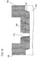
- FIG. 10 is another cross-sectional view showing the configuration after the laser-trimming fuse used in the reference example is trimmed.
- the above-described n-type well can be configured so as to come into contact with a lower surface of the insulating layer.
- the above-described n-type well can be configured so as to come into contact with a lower surface of the insulating layer.
- an upper insulating film may be provided over the semiconductor substrate and the insulating layer and a seal ring embedded into the upper insulating film so as to surround the fuse.
- the above-described p-type well can be configured to come into contact with a lower surface of the seal ring.
- the p-type well and the seal ring can be unified, to efficiently inhibit water, metal ions, organic matters, for example, from percolating into the circuit element region provided around the fuse.
- the above-described insulating layer may be made of an element separation film embedded on the element formation surface side of the semiconductor substrate.
- a particular well structure is provided below the fuse, so that when melting the fuse by laser irradiation, it is possible to inhibit water, metal ions, organic matters, for example, that have percolated from a damaged portion of for example, the insulating layer from percolating to an outside of the well structure.
- a protection insulating film may further be provided so as to cover an upper surface of the above-described fuse.
- the protection insulating film covers the upper surface of the fuse to inhibit percolation of water, metal ions, organic matters and the like, to enable inhibiting these from percolating into a region under the fuse.
- FIG. 1 is a cross-sectional view of a configuration of a laser-trimming fuse used in the present embodiment.
- a semiconductor device comprises a p-type silicon substrate 120 (semiconductor substrate). On the silicon substrate 120 , a field oxide film 101 (insulating layer) is provided.
- the field oxide film 101 is an element separation film (STI) made of an SiO 2 film embedded on the element formation surface side of the silicon substrate 120 .
- STI element separation film
- two fuses 104 are provided.
- an n-type well 102 is provided directly below the fuses 104 .
- the n-type well 102 is configured so as to come into contact with a lower surface of the field oxide film 101 .
- a p-type well 103 is provided in such a manner as to surround a region directly below the fuses 104 in the silicon substrate 120 .
- An impurity concentration of the p-type well 103 is larger than that of the other p-type regions in the silicon substrate 120 .
- the present embodiment has employed a p-type substrate as the semiconductor substrate, the present invention is not limited to this; an n-type substrate (for example, n-type silicon substrate) may be employed as the semiconductor substrate.
- an n-type substrate for example, n-type silicon substrate
- the n-type well In a case where an n-type semiconductor substrate is used as the semiconductor substrate, the n-type well only needs to have a larger impurity concentration than the other n-type regions.
- an insulating film 105 is provided on the silicon substrate 120 and the field oxide film 101 .
- the insulating film 105 is provided to cover upper surfaces of the fuses 104 .
- a contact 106 is embedded so as to surround the fuses 104 .
- the insulating film 105 functions as a protection insulating film and a portion of an upper insulating film.
- a cover insulating film 108 (a portion of the upper insulating film) is provided on the insulating film 105 .
- the cover insulating film 108 is provided so as to surround the fuses 104 .
- the upper insulating film comprises the cover insulating film 108 and a portion of the insulating film 105 .
- an interconnection 107 is embedded so as to surround the fuses 104 .
- a seal ring is comprised of the contact 106 and the interconnection 107 .
- the p-type well 103 is configured so as to come into contact with a lower surface of the seal ring.
- the cover insulating film 108 and the insulating film 105 are removed partially, to form a fuse opening.
- an oxide film, a nitride film, or an oxy-nitride film may be formed as the insulating film 105 .
- a nitride film and an oxy-nitride film in particular, have an elaborate film quality and so have a high functionality as the insulating film 105 .
- FIG. 2 is a plan view of the configuration of the laser-trimming fuse used in the present embodiment.
- the semiconductor device comprises the two fuses 104 made of a polysilicon film.
- the fuse 104 in the present embodiment has such a structure that a narrow midsection thereof may be melt by laser irradiation to disconnect interconnections. Each of the interconnections is connected with the end of the fuse 104 . Therefore, the fuse is made of a high melting point metal film made of, for example, polysilicon, Ta, TaN, tungsten, or tungsten silicide, which easily absorbs laser and has an excellent conductivity.
- a region exposed to laser irradiation which is a midsection of these fuses 104 , may be set to a small line width of, for example, 0.5 ⁇ m-1.6 ⁇ m.
- the both ends 112 of the fuse 104 have a larger width than that of the region exposed to laser irradiation and are connected to copper interconnect lines 116 (only one of which is shown) provided in the silicon substrate (not shown) directly below them.
- a fuse opening 110 is provided where the cover insulating film (not shown) does not exist.
- a seal ring 113 composed of the metal-made contact 106 and the interconnection 107 is provided in the cover insulating film 108 (not shown) and the insulating film 105 so as to surround the fuses 104 .
- Such a semiconductor device is manufactured as follows:
- the field oxide film 101 is formed on the silicon substrate 120 .
- the n-type well 102 is formed under the field oxide film 101 by ion implantation.
- the p-type well 103 is formed so as to surround the n-type well 102 .
- a polysilicon film is formed and patterned by photolithography and etching into a desired shape to form fuses 104 made of polysilicon film.
- the insulating film 105 is formed so as to cover the fuses 104 .
- a (ring-shaped as viewed from the top) trench is formed in the insulating film 105 .
- the contact 106 is formed, and over the contact 106 the interconnection 107 is formed.
- the cover insulating film 108 is formed so as to cover the interconnection 107 and the insulating film 105 .
- the insulating film 105 and the cover insulating film 108 are removed by dry etching. Accordingly, the laser-trimming opening 110 is formed above the fuses 104 .
- the semiconductor device according to the present invention has an excellent reliability. That is, the semiconductor device according to the present invention comprises the fuses 104 subject to laser trimming, so that positively charged water, metal ions, organic matters, for example, that may percolate from a portion of the fuse 104 removed by fuse trimming can be captured by the negatively charged n-type well 102 .
- thermosetting resin such as an epoxy, molded, and heat-treated to be protected from external environments. Since the thermosetting resin contains water, metal ions, and organic matters somewhat, they may get through a removed portion of the fuse 104 and percolate into the silicon substrate 120 .
- the seal ring 113 is embedded into the cover insulating film 108 and the insulating film 105 , so that it is possible to inhibit water, metal ions, organic matters, for example, from passing through the cover insulating film 108 and the insulating film 105 , and percolating into the circuit element region provided around the fuses 104 .
- the fuses 104 are melt by laser irradiation, it is possible to inhibit water, metal ions, organic matters, for example, that have percolated from a damaged portion of the field oxide film 101 , for example, from percolating to an outside of the p-type well 103 . It is thus possible to suppress degradation in functionality of the circuit elements by arranging the circuit elements to the outside of the p-type well 103 . By this configuration, therefore, a semiconductor device having an excellent reliability can be obtained.
- a configuration of a semiconductor device according to the present embodiment is basically the same as that of the semiconductor according to the first embodiment, except that the semiconductor device according to the present embodiment employs a seal ring composed of a two-step contact and a two-step interconnection as described later.
- FIGS. 3A to 3C are process cross-sectional view showing a method of manufacturing the semiconductor device according to the present embodiment in order of its manufacturing steps.
- a field oxide film 201 is formed in a fuse element portion in order to electrically insulate device elements from each other.
- This field oxide film 201 can be formed by the same process as that of the other field oxide films that define a circuit element region.
- an n-type well 202 is formed under the field oxide film 201 by ion implantation.
- the patterned photoresist (not shown) is removed by assign or wet etching.
- a p-type well 203 is formed so as to surround the n-type well 202 , to remove the photoresist (not shown) similarly.
- the p-type well 203 is formed ring shaped as viewed from the top on a surface of a silicon substrate 220 in which elements are formed.
- n-type well 202 and the p-type well 203 can be formed by the same process as that for an n-type well and a p-type well formed in a circuit element region.
- a polysilicon film is formed and patterned by photolithography and etching into a desired shape to form two fuses 204 made of polysilicon film.
- the fuses 204 can be used a high melting point metal film made of, for example, Ta, TaN, tungsten, or tungsten silicide.
- an insulating interlayer 205 (which functions also as a protection insulating film and a upper insulating film) made of BPSG is formed. As a result, the fuses 204 are embedded in the insulating interlayer 205 .
- FIG. 4 are additional process cross-sectional views for showing the method of manufacturing the semiconductor device according to the present embodiment in order of its manufacturing steps.
- the insulating interlayer 205 is patterned by photolithography and etching to obtain a (ring-shaped as viewed from the top) trench which encircles the fuses 204 .
- a contact plug 206 is formed which is constituted of a barrier metal film made of, for example, titanium and a tungsten film provided in the barrier metal film.
- an aluminum film is formed on the insulating interlayer 205 and patterned by photolithography and etching into a first interconnection 207 that covers the contact plug 206 .
- the first interconnection 207 is made of aluminum.
- the first interconnection 207 is covered by an insulating oxide film 208 .
- a ring-shaped region of the insulating oxide film 208 (a portion of upper insulating film) directly on the first interconnection 207 is patterned by photolithography and removed by dry etching, to obtain a ring-shaped trench.
- a first via 209 (see FIG. 5 ) is formed on the first interconnection 207 .
- a laser-trimming opening 210 is formed above the fuses 204 .
- an aluminum film is formed on the insulating oxide layer 208 and patterned by photolithography and dry etching into a second interconnection 211 that covers the first via 209 .
- the second interconnection 211 is made of aluminum.
- the second interconnection 211 is covered by an insulating oxide film 212 (a portion of upper insulating film). Further, a top-layer insulating oxide film 213 is formed on an upper surface of the insulating oxide film 212 .
- the insulating oxide films 213 and 212 directly above the fuses 204 are patterned by photolithography and removed by dry etching, to form the laser-trimming opening 210 again above the fuses 204 .
- the fuse opening 210 has been formed by the same process as that for forming the ring-shaped trench for the first via 209 , the present invention is not limited to it; it may be formed by a different process.
- the insulating oxide films 213 , 212 , and 208 and the insulating interlayer 205 directly above the fuses 204 may be patterned by photolithography and removed by dry etching, to form the laser-trimming opening 210 above the fuses 204 .
- FIGS. 5 and 6 are cross-sectional views of a configuration after the laser-trimming fuse used in the present embodiment is trimmed.
- the semiconductor device according to the present invention is also excellent in reliability similar to that according to the first embodiment. That is, in the semiconductor device according to the present embodiment, as shown in FIG. 5 , positively charged water, metal ions, organic matters, for example, that have percolated from a portion where the fuses 204 are removed by laser are captured by the negatively charged n-type well 202 . Further, even if positively charged water, metal ions, organic matters, for example, have percolated to the outside of the n-type well 202 , the positively charged water, metal ions, organic matters, for example, are brought back to the n-type well 202 owing to a difference in potential between the negatively charged n-type well 202 and the positively charged p-type well 203 . Accordingly, the water, metal ions, organic matters, for example, are inhibited from percolating to semiconductor elements arranged outside the p-type well 203 .
- the contact plug 206 constituted of a barrier metal made of, for example, titanium and a tungsten film provided in the barrier metal film, it is possible to inhibit the above-described water, metal ions, organic matters, for example, from percolating from a lower surface of the first interconnection 207 . Therefore, by arranging, for example, circuit elements outside the p-type well 203 , it is possible to suppress degradation in functionality of the circuit elements. By this configuration, therefore, a semiconductor excellent in reliability can be obtained.
- the silicon substrate 220 is typically grounded in potential.
- melting of the fuses 204 by use of laser irradiation is performed by heating and damaging the polysilicon film of the fuses 204 . Therefore, when the fuses 204 are melt, the field oxide film 201 may be damaged and removed as shown in FIG. 6 . In such a case, since the fuses 204 and the field oxide film 201 are removed, positively charged water, metal ions, and organic matters easily percolate into the silicate substrate. However, the positively charged water, metal ions, and organic matters are captured by the negatively charged n-type well 202 .
- the positively charged water, metal ions, organic matters for example, have percolated to the outside of the n-type well 202 , the positively charged water, metal ions, organic matters, for example, are brought back to the n-type well 202 owing to a difference in potential between the negatively charged n-type well 202 and the positively charged p-type well 203 . It is thus possible to suppress degradation in functionality of the circuit elements arranged outside the p-type well.
- the present invention works especially in a case where a fuse is melt by laser irradiation.
- a seal ring constituted of two contact plugs and two interconnections is used, so that it is possible to further securely inhibit water, metal ions, organic matters, for example, from percolating to a circuit element region arranged around the fuse 104 .
- the semiconductor device according to the present embodiment is excellent in manufacturing stability. That is, according to a configuration of the semiconductor device according to the present embodiment, it is possible to load a laser-trimming fuse element especially, for example, into a high-quality, vehicle-installed semiconductor device which operates in a severe environment and whose defective fraction is required to be lppm or less.
- the present configuration in which the fuses 204 are provided on the field oxide film 201 on the silicon substrate 220 , is excellent in combination with a basic CMOS transistor manufacturing process. It is, therefore, possible to form the fuses 204 without adding any manufacturing process to the basic CMOS transistor manufacturing process, thereby further enhancing added values of the high-quality semiconductor device.
- the present invention therefore, can be easily applied to a variety of configurations of semiconductor devices, thereby improving manufacturing stability of semiconductors including reduction in rejection in the market and improvements in yield thereof.
- FIG. 8 is a cross-sectional view of a configuration of a laser-trimming fuse used in the reference example.
- a fuse 704 made of generally polysilicon is formed on a field oxide film 701 , and a protection oxide film 705 is formed thereon. Further, a fuse opening 710 is formed by removing the protection oxide film 705 on the fuses 704 through dry etching to a desired film thickness so that the fuses 704 can be melt easily.
- FIGS. 9 and 10 are cross-sectional views of a configuration after the laser-trimming fuse used in the reference example is trimmed.
- a damaged portion 715 given after the fuse 704 is trimmed (removed) has such a structure that the fuse 704 and a portion of the protection oxide film 705 thereon are removed and, therefore, is opened down to the field oxide film 701 .
- thermosetting resin such as an epoxy, molded, and heat-treated to be protected from external environments.
- the thermosetting resin before molding contains water, metal ions, and resin somewhat.
- the damaged portion 715 given after the fuse 204 is removed has a smaller thickness of the protection oxide film 705 than the other portions. Therefore, when the fuse opening 710 is filled with the thermosetting resin thereafter, a distance between a silicon substrate 720 and the thermosetting resin at the damaged portion 715 is smaller than those at the other portions. In this case, it is difficult to capture the water, metal ions, and organic matters from the heat-hardening resin by using the protection oxide film 705 at the damaged portion 715 .
- thermosetting resin water, metal ions, and organic matters from the thermosetting resin are more easily to percolate into the silicon substrate.
- the silicon substrate since no well is provided below the removed fuse 704 , if the silicon substrate is a p-type one, the water, metal ions, and organic matters that have percolated into the silicon substrate cannot be captured. Even in a case where the silicon substrate is an n-type one, since no well is formed and the substrate has a uniform potential everywhere therein, the water, metal ions, and organic matters that have percolated into the silicon substrate cannot be captured. Therefore, the water, metal ions, and organic matters are liable to reach a circuit element region. The percolation of the water, metal ions, and organic matters causes malfunctioning of a semiconductor device and deteriorates its reliability.
- a sidewall of the fuse opening 710 is not covered by a protection nitride film. Further, no seal ring is provided deep in the sidewall of the fuse opening 710 . Therefore, there is a slight possibility that laser irradiation may damage the protection oxide film 705 at the sidewall so that its function as a protection film may be deteriorated.
- a particular well structure directly below the fuses and a seal ring enable inhibiting organic matters, metal ions, and water from, for example, sealing resin in contact with the fuse opening subject to trimming from percolating into a region of semiconductor elements. It is thus possible to provide a fuse structure that can secure a high reliability for, for example, a vehicle-installed semiconductor device.
- materials of the cover insulating film 108 , the insulating film 105 , the insulating interlayer 205 , and the insulating oxide films 208 , 212 , and 213 are not limited in particular; for example, an SiO 2 film, an SiN film, or an SiON film can be used optimally.
- an SiN film or an SiON film By using an SiN film or an SiON film in particular, a merit which improves waterproof properties of the insulating films themselves may be obtained.
- n-type well and a p-type well have been formed in a silicon substrate, only one of them may be formed instead.
Landscapes
- Design And Manufacture Of Integrated Circuits (AREA)
- Internal Circuitry In Semiconductor Integrated Circuit Devices (AREA)
Abstract
Description
Claims (20)
Applications Claiming Priority (4)
| Application Number | Priority Date | Filing Date | Title |
|---|---|---|---|
| JP2004-311284 | 2004-10-26 | ||
| JP2004311284 | 2004-10-26 | ||
| JP2005287792A JP2006156960A (en) | 2004-10-26 | 2005-09-30 | Semiconductor device |
| JP2005-287792 | 2005-09-30 |
Publications (2)
| Publication Number | Publication Date |
|---|---|
| US20060087002A1 US20060087002A1 (en) | 2006-04-27 |
| US8729663B2 true US8729663B2 (en) | 2014-05-20 |
Family
ID=36205445
Family Applications (1)
| Application Number | Title | Priority Date | Filing Date |
|---|---|---|---|
| US11/244,161 Active 2027-01-05 US8729663B2 (en) | 2004-10-26 | 2005-10-06 | Semiconductor device |
Country Status (4)
| Country | Link |
|---|---|
| US (1) | US8729663B2 (en) |
| JP (1) | JP2006156960A (en) |
| KR (1) | KR100767037B1 (en) |
| TW (1) | TWI297528B (en) |
Families Citing this family (7)
| Publication number | Priority date | Publication date | Assignee | Title |
|---|---|---|---|---|
| US7615841B2 (en) * | 2005-05-02 | 2009-11-10 | Taiwan Semiconductor Manufacturing Company, Ltd. | Design structure for coupling noise prevention |
| JP2012033894A (en) | 2010-06-30 | 2012-02-16 | Canon Inc | Solid state image sensor |
| JP6342033B2 (en) * | 2010-06-30 | 2018-06-13 | キヤノン株式会社 | Solid-state imaging device |
| JP5981260B2 (en) * | 2011-09-30 | 2016-08-31 | エスアイアイ・セミコンダクタ株式会社 | Semiconductor device |
| JP2017045839A (en) | 2015-08-26 | 2017-03-02 | ルネサスエレクトロニクス株式会社 | Semiconductor device |
| JP6926806B2 (en) * | 2017-08-09 | 2021-08-25 | 富士電機株式会社 | Semiconductor devices and their manufacturing methods |
| US11355433B2 (en) * | 2019-10-02 | 2022-06-07 | Semiconductor Components Industries, Llc | Semiconductor fuse structure and method of manufacturing a semiconductor fuse structure |
Citations (14)
| Publication number | Priority date | Publication date | Assignee | Title |
|---|---|---|---|---|
| US4723155A (en) * | 1981-10-09 | 1988-02-02 | Tokyo Shibaura Denki Kabushiki Kaisha | Semiconductor device having a programmable fuse element |
| JPS6480037A (en) | 1987-09-19 | 1989-03-24 | Hitachi Ltd | Semiconductor integrated circuit device |
| JPH0563091A (en) | 1991-09-04 | 1993-03-12 | Fujitsu Ltd | Semiconductor device |
| JPH06204340A (en) | 1993-01-06 | 1994-07-22 | Rohm Co Ltd | Trimming fuse structure of semiconductor device |
| JPH10223762A (en) | 1997-02-07 | 1998-08-21 | Nec Corp | Semiconductor device and manufacturing method thereof |
| US5854510A (en) * | 1996-12-27 | 1998-12-29 | Vlsi Technology, Inc. | Low power programmable fuse structures |
| JPH11233722A (en) | 1998-02-12 | 1999-08-27 | Nec Ic Microcomput Syst Ltd | FUSE DEVICE AND ITS MANUFACTURING METHOD |
| US6100118A (en) * | 1998-06-11 | 2000-08-08 | Taiwan Semiconductor Manufacturing Company, Ltd. | Fabrication of metal fuse design for redundancy technology having a guard ring |
| US6319758B1 (en) * | 1999-06-10 | 2001-11-20 | Taiwan Semiconductor Manufacturing Company | Redundancy structure in self-aligned contact process |
| US20020004932A1 (en) * | 2000-03-27 | 2002-01-10 | Jeng-Jye Shau | Cost saving methods using pre-defined integrated circuit modules |
| US6410367B2 (en) | 1999-04-16 | 2002-06-25 | Micron Technology, Inc. | Fuse for use in a semiconductor device, and semiconductor devices including the fuse |
| US6469354B1 (en) * | 1998-03-24 | 2002-10-22 | Nec Corporation | Semiconductor device having a protective circuit |
| US6879023B1 (en) * | 2000-03-22 | 2005-04-12 | Broadcom Corporation | Seal ring for integrated circuits |
| US20050110070A1 (en) * | 2003-10-24 | 2005-05-26 | Masayoshi Omura | Semiconductor device with capacitor and fuse and its manufacture method |
-
2005
- 2005-09-30 JP JP2005287792A patent/JP2006156960A/en active Pending
- 2005-10-06 US US11/244,161 patent/US8729663B2/en active Active
- 2005-10-13 TW TW094135666A patent/TWI297528B/en not_active IP Right Cessation
- 2005-10-25 KR KR1020050100861A patent/KR100767037B1/en not_active Expired - Fee Related
Patent Citations (17)
| Publication number | Priority date | Publication date | Assignee | Title |
|---|---|---|---|---|
| US4723155A (en) * | 1981-10-09 | 1988-02-02 | Tokyo Shibaura Denki Kabushiki Kaisha | Semiconductor device having a programmable fuse element |
| JPS6480037A (en) | 1987-09-19 | 1989-03-24 | Hitachi Ltd | Semiconductor integrated circuit device |
| US5990537A (en) * | 1991-09-04 | 1999-11-23 | Fujitsu Limited | Semiconductor device with fuse |
| JPH0563091A (en) | 1991-09-04 | 1993-03-12 | Fujitsu Ltd | Semiconductor device |
| JPH06204340A (en) | 1993-01-06 | 1994-07-22 | Rohm Co Ltd | Trimming fuse structure of semiconductor device |
| US5854510A (en) * | 1996-12-27 | 1998-12-29 | Vlsi Technology, Inc. | Low power programmable fuse structures |
| JPH10223762A (en) | 1997-02-07 | 1998-08-21 | Nec Corp | Semiconductor device and manufacturing method thereof |
| US6373120B1 (en) * | 1998-02-12 | 2002-04-16 | Nec Corporation | Semiconductor device for simultaneously achieving high reliability to laser light radiation and small occupation region and method of manufacturing it |
| TW418521B (en) | 1998-02-12 | 2001-01-11 | Nippon Electric Co | Semiconductor device for simultaneously achieving high reliability to laser light radiation and small occupation region and method of manufacturing it |
| JPH11233722A (en) | 1998-02-12 | 1999-08-27 | Nec Ic Microcomput Syst Ltd | FUSE DEVICE AND ITS MANUFACTURING METHOD |
| US6469354B1 (en) * | 1998-03-24 | 2002-10-22 | Nec Corporation | Semiconductor device having a protective circuit |
| US6100118A (en) * | 1998-06-11 | 2000-08-08 | Taiwan Semiconductor Manufacturing Company, Ltd. | Fabrication of metal fuse design for redundancy technology having a guard ring |
| US6410367B2 (en) | 1999-04-16 | 2002-06-25 | Micron Technology, Inc. | Fuse for use in a semiconductor device, and semiconductor devices including the fuse |
| US6319758B1 (en) * | 1999-06-10 | 2001-11-20 | Taiwan Semiconductor Manufacturing Company | Redundancy structure in self-aligned contact process |
| US6879023B1 (en) * | 2000-03-22 | 2005-04-12 | Broadcom Corporation | Seal ring for integrated circuits |
| US20020004932A1 (en) * | 2000-03-27 | 2002-01-10 | Jeng-Jye Shau | Cost saving methods using pre-defined integrated circuit modules |
| US20050110070A1 (en) * | 2003-10-24 | 2005-05-26 | Masayoshi Omura | Semiconductor device with capacitor and fuse and its manufacture method |
Non-Patent Citations (2)
| Title |
|---|
| Japanese Official Action mailed Feb. 1, 2011 in corresponding Japanese Application No. 2005-287792 with English translation. |
| Notice of Reasons for Refusal dated Oct. 16, 2012 issued by Japanese Patent Office in Japanese Patent Application No. 2011-24612, with English translation. |
Also Published As
| Publication number | Publication date |
|---|---|
| TWI297528B (en) | 2008-06-01 |
| KR100767037B1 (en) | 2007-10-15 |
| TW200623328A (en) | 2006-07-01 |
| US20060087002A1 (en) | 2006-04-27 |
| JP2006156960A (en) | 2006-06-15 |
| KR20060049348A (en) | 2006-05-18 |
Similar Documents
| Publication | Publication Date | Title |
|---|---|---|
| US8106514B2 (en) | Semiconductor device having an annular guard ring | |
| JP4502173B2 (en) | Semiconductor device and manufacturing method thereof | |
| JP5324822B2 (en) | Semiconductor device | |
| US6498089B2 (en) | Semiconductor integrated circuit device with moisture-proof ring and its manufacture method | |
| US6255151B1 (en) | Semiconductor integrated circuit device and method of manufacturing same | |
| JP5622433B2 (en) | Semiconductor device and manufacturing method thereof | |
| US20060145347A1 (en) | Semiconductor device and method for fabricating the same | |
| US7932602B2 (en) | Metal sealed wafer level CSP | |
| US9659861B2 (en) | Semiconductor device and fabrication method thereof | |
| US20090121322A1 (en) | Semiconductor chip and semiconductor device | |
| US8228158B2 (en) | Semiconductor device | |
| US12046527B2 (en) | Planar passivation layers | |
| KR100791339B1 (en) | Composite chip semiconductor device including planarization resistance pattern and manufacturing method | |
| CN107305872B (en) | Protection against premature breakdown of interline porous dielectrics in integrated circuits | |
| US8729663B2 (en) | Semiconductor device | |
| US20030173597A1 (en) | Semiconductor device | |
| US6291281B1 (en) | Method of fabricating protection structure | |
| KR101586270B1 (en) | Semiconductor device including fuse | |
| CN100508181C (en) | Semiconductor device | |
| JP2007027639A (en) | Semiconductor device | |
| US20140183741A1 (en) | Mask read-only memory (rom) and method for fabricating the same | |
| EP2790211B1 (en) | Method of producing a through-substrate via in a semiconductor device and semiconductor device comprising a through-substrate via | |
| JP5632766B2 (en) | Semiconductor device | |
| JP2008053320A (en) | Semiconductor device and manufacturing method thereof | |
| US7566594B2 (en) | Fabricating method of semiconductor device |
Legal Events
| Date | Code | Title | Description |
|---|---|---|---|
| AS | Assignment |
Owner name: NEC ELECTRONICS CORPORATION, JAPAN Free format text: ASSIGNMENT OF ASSIGNORS INTEREST;ASSIGNORS:MIWA, KIYOTAKA;KARIYA, NAYUTA;REEL/FRAME:017079/0977 Effective date: 20050930 |
|
| AS | Assignment |
Owner name: RENESAS ELECTRONICS CORPORATION, JAPAN Free format text: CHANGE OF NAME;ASSIGNOR:NEC ELECTRONICS CORPORATION;REEL/FRAME:025346/0877 Effective date: 20100401 |
|
| STCF | Information on status: patent grant |
Free format text: PATENTED CASE |
|
| MAFP | Maintenance fee payment |
Free format text: PAYMENT OF MAINTENANCE FEE, 4TH YEAR, LARGE ENTITY (ORIGINAL EVENT CODE: M1551) Year of fee payment: 4 |
|
| AS | Assignment |
Owner name: RENESAS ELECTRONICS CORPORATION, JAPAN Free format text: CHANGE OF ADDRESS;ASSIGNOR:RENESAS ELECTRONICS CORPORATION;REEL/FRAME:044928/0001 Effective date: 20150806 |
|
| MAFP | Maintenance fee payment |
Free format text: PAYMENT OF MAINTENANCE FEE, 8TH YEAR, LARGE ENTITY (ORIGINAL EVENT CODE: M1552); ENTITY STATUS OF PATENT OWNER: LARGE ENTITY Year of fee payment: 8 |
|
| FEPP | Fee payment procedure |
Free format text: MAINTENANCE FEE REMINDER MAILED (ORIGINAL EVENT CODE: REM.); ENTITY STATUS OF PATENT OWNER: LARGE ENTITY |