US8717067B2 - Method and apparatus for continuous-averaging counter-based digital frequency lock detector - Google Patents
Method and apparatus for continuous-averaging counter-based digital frequency lock detector Download PDFInfo
- Publication number
- US8717067B2 US8717067B2 US11/068,225 US6822505A US8717067B2 US 8717067 B2 US8717067 B2 US 8717067B2 US 6822505 A US6822505 A US 6822505A US 8717067 B2 US8717067 B2 US 8717067B2
- Authority
- US
- United States
- Prior art keywords
- counter
- target
- clock
- frequency offset
- violation
- Prior art date
- Legal status (The legal status is an assumption and is not a legal conclusion. Google has not performed a legal analysis and makes no representation as to the accuracy of the status listed.)
- Expired - Fee Related, expires
Links
Images


Classifications
-
- H—ELECTRICITY
- H03—ELECTRONIC CIRCUITRY
- H03L—AUTOMATIC CONTROL, STARTING, SYNCHRONISATION, OR STABILISATION OF GENERATORS OF ELECTRONIC OSCILLATIONS OR PULSES
- H03L7/00—Automatic control of frequency or phase; Synchronisation
- H03L7/06—Automatic control of frequency or phase; Synchronisation using a reference signal applied to a frequency- or phase-locked loop
- H03L7/08—Details of the phase-locked loop
- H03L7/085—Details of the phase-locked loop concerning mainly the frequency- or phase-detection arrangement including the filtering or amplification of its output signal
- H03L7/095—Details of the phase-locked loop concerning mainly the frequency- or phase-detection arrangement including the filtering or amplification of its output signal using a lock detector
-
- H—ELECTRICITY
- H04—ELECTRIC COMMUNICATION TECHNIQUE
- H04J—MULTIPLEX COMMUNICATION
- H04J3/00—Time-division multiplex systems
- H04J3/02—Details
- H04J3/06—Synchronising arrangements
- H04J3/0635—Clock or time synchronisation in a network
- H04J3/0685—Clock or time synchronisation in a node; Intranode synchronisation
Definitions
- the present invention relates generally to frequency lock detection circuits, and more particularly, to digital frequency lock detectors.
- Clock recovery circuits and their associated frequency lock detection circuits are widely used, for example, in modern communications systems.
- Frequency lock detectors are used, for example, to obtain clock tolerance and offset information.
- Counter-based digital frequency lock detectors obtain clock offset information at fixed or programmable time intervals. Clock offset information is used in many applications, such as tuning clock generators.
- a counter-based digital frequency lock detector contains two equal-length counters. A first counter, generally referred to as the target counter, is clocked by the target clock.
- a second counter is clocked by a reference clock.
- the counter-based digital frequency lock detector ensures that the target clock stays within a desired tolerance of the reference clock.
- a system such as a SONET optical ring network
- both counters are initialized with the same initial count before starting to count. For example, if “up” counters are used, the initial count is set to zero.
- the reference counter reaches a predefined count, such as 10,000, the value of the target counter is evaluated. If the target counter has a value between 9999 ( ⁇ 100 ppm) and 10001 (+100 ppm), the target clock has satisfied the 100 ppm offset requirement.
- the output of the counter-based digital frequency lock detector is updated when the reference counter reaches the predefined count, and the target counter is examined to determine if the target counter value falls within a certain tolerance range.
- the tolerance range or offset range is an integer obtained by subtracting the maximum negative PPM count from the minimum positive PPM count.
- the predefined count is typically a very large number and the frequency offset cannot be determined until the reference counter reaches this large number.
- the frequency offset status output can only change at a fixed time interval, which may not be desirable in applications where prompt detection is required. A need therefore exists for a counter-based digital frequency lock detector that can evaluate a frequency offset more quickly than such conventional designs.
- a counter-based digital frequency lock detector in accordance with the present invention comprises a reference counter clocked by a reference clock and a target counter clocked by a target clock.
- the target counter is n bits and n is less than a number of bits of the reference counter.
- a frequency offset violation of the target clock is detected by comparing a value of the target counter to an n bit counter.
- a frequency offset violation occurs when the target clock has a frequency offset relative to the reference clock that violates a predefined threshold.
- the frequency offset violation can be detected by comparing the target counter to a second n bit reference counter clocked by the reference clock.
- the frequency offset violation is detected by comparing the target counter to n least significant bits of the reference counter.
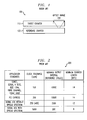
- FIG. 1 illustrates a conventional counter-based digital frequency lock detector
- FIG. 2 is a sample table illustrating clock tolerance, output interval and counter length requirements for a number of well known communication standards
- FIG. 3 illustrates a continuous averaging counter-based digital frequency lock detector incorporating features of the present invention
- FIG. 4 illustrates an alternate continuous averaging counter-based digital frequency lock detector incorporating features of the present invention.
- the present invention provides a counter-based digital frequency lock detector that can evaluate a frequency offset more quickly than such conventional designs.
- the present invention recognizes that although a number of standards, such as SONET and PCI Express require the reference and target counters to have a length between 8 and 14 bits, the tolerance range on the frequency offset is typically only 2 to 3 bits.
- FIG. 1 illustrates a conventional counter-based digital frequency lock detector 100 .
- the exemplary counter-based digital frequency lock detector 100 comprises two equal-length counters 110 , 120 .
- the target counter 110 is clocked by the target clock and the reference counter 120 is clocked by a reference clock.
- the counter-based digital frequency lock detector 100 ensures that the target clock stays within a desired tolerance of the reference clock.
- the counters 110 , 120 are initialized with the same initial count before starting to count. When the reference counter 120 reaches a predefined count, such as 10,000, the value of the target counter 110 is evaluated. Upon evaluation, the value of the target counter 110 must be within a specified offset range 150 .
- FIG. 2 is a sample table illustrating clock tolerance, output interval and counter length requirements for a number of well known communication standards. As shown in FIG. 2 , the standards typically require the length of the counters 110 , 120 to be 8 to 14 bits.
- continuous averaging techniques are applied to counter-based digital frequency lock detectors.
- the disclosed technique is both area-efficient and robust. For example, an exemplary implementation has demonstrated 25% to 38% reductions in area in Taiwan Semiconductor Manufacturing Corporation (TSMC) 0.13 um technology, relative to conventional designs.
- TSMC Taiwan Semiconductor Manufacturing Corporation
- the continuous averaging counter-based digital frequency lock detectors of the present invention can detect certain transient out-of-range offset errors with no added overheads. Further, the disclosed detectors can restart as soon as a definite output is obtained, rather than outputting a value only at a fixed time interval. Thus, the disclosed detectors provide quicker system response for certain applications.
- FIG. 3 illustrates a continuous averaging counter-based digital frequency lock detector 300 incorporating features of the present invention.
- the continuous averaging counter-based digital frequency lock detector 300 comprises a longer reference counter 330 clocked by reference clock, and two smaller counters 310 , 320 .
- the continuous averaging counter-based digital frequency lock detector 300 using only a single long counter 330 , compared to the two long counters 110 , 120 of the conventional design of FIG. 1 .
- One small counter 310 is clocked by the target clock and the second small counter 320 , referred to as the reference counter, is clocked by the reference clock.
- the two small counters 310 , 320 are offset to fit the tolerance range at initialization. If frequency lock has a balanced PPM requirement, i.e., +PPM and ⁇ PPM are identical, then the two pointers will be placed exactly a half tolerance range apart. If frequency lock has an unbalanced PPM requirement, as in the case of many spread spectrum applications, where +PPM is not equal to ⁇ PPM, the distance between the two pointers will be separated based on the ratio between +PPM and ⁇ PPM.
- the counters 310 , 320 can be considered first-in-first-out (FIFO) pointers.
- the range of the FIFO is equal to the offset range.
- Both counters 310 , 320 have the same count direction, i.e., both counters count up or both counters count down. When the pointer reaches the end, the counter will loop around and continue the same count direction again, unless the counter is stopped by a reset. For example, consider a 3-bit counter counting from 0 upwards to 7. Once the counter reaches 7, the next count will be 0, next 1, 2, and so on. A “FIFO” overflow occurs when the two counters have the same count, because the pointers have been initialized to different counts. Should there be no frequency difference, the two counters will never have the same count.
- the target pointer catches the reference pointer, the target clock is too fast (a +PPM violation). If the reference pointer catches the target pointer, the target clock is too slow (a ⁇ PPM violation). A “FIFO” overflow will set the status bit to indicate that the target clock has violated the frequency lock requirement.
- the “FIFO” counter will overflow before the long counter 330 reaches the predefined value. It is noted that the overflow cannot be masked by an opposite offset later in time to achieve average offset within tolerance. In the prior art, this type of frequency lock violation can go without being detected. This is also a significant part of the motivation for the current design.
- a threshold violation on the frequency offset can be immediately detected.
- the detector 300 can restart, rather than waiting for the full count to be reached. This allows for a quick system response in certain applications.
- the disclosed continuous averaging technique enables more reliable detection, and early detection and shorter output latency, should the target clock 310 run outside the desired tolerance range.
- this type of transient offset error can be hidden, since counter can only detect offset at the end of count.
- the disclosed continuous averaging architecture detects clock offsets in decreasing order until the targeted tolerance is reached at the end of the long count.
- the use of the two small counters 310 , 320 uses fewer bits than the long counter 330 , resulting in area, power, and cost savings, relative to the conventional design 100 .
- FIG. 4 illustrates an alternate continuous averaging counter-based digital frequency lock detector 400 incorporating features of the present invention.
- the continuous averaging counter-based digital frequency lock detector 400 modifies the implementation of FIG. 3 by “folding” the small counter 420 of the reference clock into least significant bits (LSB) of the long counter 430 , which is also clocked by the reference clock. Therefore, the disclosed continuous averaging architecture can be realized with one long counter 430 and one small counter 410 (providing a virtual triple counter but using only two counters).
- the length of the small counter 410 is typically fixed, representing the tolerance range.
- the length of the long counter 430 is set by the clock tolerance requirement.
- the value of the small counter 410 is evaluated when the LSBs of the long counter 430 reach the predefined value.
- the embodiment of FIG. 4 provides further area, power and cost improvements.
- a plurality of identical die are typically formed in a repeated pattern on a surface of the wafer.
- Each die includes a device described herein, and may include other structures or circuits.
- the individual die are cut or diced from the wafer, then packaged as an integrated circuit.
- One skilled in the art would know how to dice wafers and package die to produce integrated circuits. Integrated circuits so manufactured are considered part of this invention.
Abstract
Description
Claims (17)
Priority Applications (1)
| Application Number | Priority Date | Filing Date | Title |
|---|---|---|---|
| US11/068,225 US8717067B2 (en) | 2005-02-28 | 2005-02-28 | Method and apparatus for continuous-averaging counter-based digital frequency lock detector |
Applications Claiming Priority (1)
| Application Number | Priority Date | Filing Date | Title |
|---|---|---|---|
| US11/068,225 US8717067B2 (en) | 2005-02-28 | 2005-02-28 | Method and apparatus for continuous-averaging counter-based digital frequency lock detector |
Publications (2)
| Publication Number | Publication Date |
|---|---|
| US20060192593A1 US20060192593A1 (en) | 2006-08-31 |
| US8717067B2 true US8717067B2 (en) | 2014-05-06 |
Family
ID=36931465
Family Applications (1)
| Application Number | Title | Priority Date | Filing Date |
|---|---|---|---|
| US11/068,225 Expired - Fee Related US8717067B2 (en) | 2005-02-28 | 2005-02-28 | Method and apparatus for continuous-averaging counter-based digital frequency lock detector |
Country Status (1)
| Country | Link |
|---|---|
| US (1) | US8717067B2 (en) |
Families Citing this family (2)
| Publication number | Priority date | Publication date | Assignee | Title |
|---|---|---|---|---|
| US7714667B2 (en) * | 2007-11-02 | 2010-05-11 | Agere Systems Inc. | Programmable linear trimming method and system for phase locked loop circuit calibration |
| US7696798B2 (en) * | 2008-02-08 | 2010-04-13 | Sun Microsystems, Inc. | Method and apparatus to generate system clock synchronization pulses using a PLL lock detect signal |
Citations (5)
| Publication number | Priority date | Publication date | Assignee | Title |
|---|---|---|---|---|
| US4691330A (en) * | 1985-03-29 | 1987-09-01 | Sumitomo Electric Industries, Ltd. | Duty control circuit for gradually reducing the duty time |
| US4715050A (en) * | 1986-03-31 | 1987-12-22 | Kabushiki Kaisha Toshiba | Digital phase-locked loop circuit |
| US6320469B1 (en) * | 2000-02-15 | 2001-11-20 | Agere Systems Guardian Corp. | Lock detector for phase-locked loop |
| US20050140418A1 (en) * | 2003-12-31 | 2005-06-30 | Ravisangar Muniandy | On-chip frequency degradation compensation |
| US7242229B1 (en) * | 2001-05-06 | 2007-07-10 | Altera Corporation | Phase locked loop (PLL) and delay locked loop (DLL) counter and delay element programming in user mode |
-
2005
- 2005-02-28 US US11/068,225 patent/US8717067B2/en not_active Expired - Fee Related
Patent Citations (5)
| Publication number | Priority date | Publication date | Assignee | Title |
|---|---|---|---|---|
| US4691330A (en) * | 1985-03-29 | 1987-09-01 | Sumitomo Electric Industries, Ltd. | Duty control circuit for gradually reducing the duty time |
| US4715050A (en) * | 1986-03-31 | 1987-12-22 | Kabushiki Kaisha Toshiba | Digital phase-locked loop circuit |
| US6320469B1 (en) * | 2000-02-15 | 2001-11-20 | Agere Systems Guardian Corp. | Lock detector for phase-locked loop |
| US7242229B1 (en) * | 2001-05-06 | 2007-07-10 | Altera Corporation | Phase locked loop (PLL) and delay locked loop (DLL) counter and delay element programming in user mode |
| US20050140418A1 (en) * | 2003-12-31 | 2005-06-30 | Ravisangar Muniandy | On-chip frequency degradation compensation |
Non-Patent Citations (1)
| Title |
|---|
| U.S. Appl. No. 11/053,365, filed Feb. 8, 2005, Dai et al. |
Also Published As
| Publication number | Publication date |
|---|---|
| US20060192593A1 (en) | 2006-08-31 |
Similar Documents
| Publication | Publication Date | Title |
|---|---|---|
| US7884751B2 (en) | Time-to-digital converter | |
| US7872602B2 (en) | Time to digital converting circuit and related method | |
| US10782763B2 (en) | Semiconductor device | |
| US6411130B1 (en) | Method and system for reliably providing a lock indication | |
| CN110520745B (en) | Estimating timing relaxation using endpoint critical sensor circuit | |
| US8717067B2 (en) | Method and apparatus for continuous-averaging counter-based digital frequency lock detector | |
| EP1237282A1 (en) | Circuit for the detection of clock signal period abnormalities | |
| US7734672B2 (en) | Checking of a bit flow | |
| US8724762B2 (en) | Clock regeneration method, reference-less receiver, and crystal-less system | |
| US20190280697A1 (en) | Delay circuit | |
| US20030172327A1 (en) | Circuit and method for testing embedded phase-locked loop circuit | |
| US8283983B2 (en) | Frequency calibration device and method for programmable oscillator | |
| US6960960B2 (en) | Frequency detector detecting variation in frequency difference between data signal and clock signal | |
| US11482992B2 (en) | Clock sweeping system | |
| US7412640B2 (en) | Self-synchronizing pseudorandom bit sequence checker | |
| US8907730B2 (en) | Frequency calibration device and method for programmable oscillator | |
| CN101702642A (en) | Method for detecting SDH frame headers | |
| CN115129296A (en) | True random number generator and true random number generation method | |
| CN110763974B (en) | Surge measuring device and method | |
| US20070159213A1 (en) | Method and apparatus for measuring and compensating for static phase error in phase locked loops | |
| US7750831B2 (en) | Phase detector utilizing analog-to-digital converter components | |
| CN111273726B (en) | Duty ratio deviation compensation circuit, method and chip | |
| TWI710770B (en) | Glitch measurement device and glitch measurement method | |
| US7173493B1 (en) | Range controller circuit and method | |
| JP5171379B2 (en) | Frequency abnormality detection circuit |
Legal Events
| Date | Code | Title | Description |
|---|---|---|---|
| AS | Assignment |
Owner name: AGERE SYSTEMS INC., PENNSYLVANIA Free format text: ASSIGNMENT OF ASSIGNORS INTEREST;ASSIGNOR:DAI, XINGDONG;REEL/FRAME:016448/0914 Effective date: 20050318 |
|
| AS | Assignment |
Owner name: AGERE SYSTEMS LLC, PENNSYLVANIA Free format text: CERTIFICATE OF CONVERSION;ASSIGNOR:AGERE SYSTEMS INC.;REEL/FRAME:032341/0415 Effective date: 20120730 |
|
| STCF | Information on status: patent grant |
Free format text: PATENTED CASE |
|
| AS | Assignment |
Owner name: DEUTSCHE BANK AG NEW YORK BRANCH, AS COLLATERAL AG Free format text: PATENT SECURITY AGREEMENT;ASSIGNORS:LSI CORPORATION;AGERE SYSTEMS LLC;REEL/FRAME:032856/0031 Effective date: 20140506 |
|
| AS | Assignment |
Owner name: AVAGO TECHNOLOGIES GENERAL IP (SINGAPORE) PTE. LTD Free format text: ASSIGNMENT OF ASSIGNORS INTEREST;ASSIGNOR:AGERE SYSTEMS LLC;REEL/FRAME:035365/0634 Effective date: 20140804 |
|
| AS | Assignment |
Owner name: AGERE SYSTEMS LLC, PENNSYLVANIA Free format text: TERMINATION AND RELEASE OF SECURITY INTEREST IN PATENT RIGHTS (RELEASES RF 032856-0031);ASSIGNOR:DEUTSCHE BANK AG NEW YORK BRANCH, AS COLLATERAL AGENT;REEL/FRAME:037684/0039 Effective date: 20160201 Owner name: LSI CORPORATION, CALIFORNIA Free format text: TERMINATION AND RELEASE OF SECURITY INTEREST IN PATENT RIGHTS (RELEASES RF 032856-0031);ASSIGNOR:DEUTSCHE BANK AG NEW YORK BRANCH, AS COLLATERAL AGENT;REEL/FRAME:037684/0039 Effective date: 20160201 |
|
| AS | Assignment |
Owner name: BANK OF AMERICA, N.A., AS COLLATERAL AGENT, NORTH CAROLINA Free format text: PATENT SECURITY AGREEMENT;ASSIGNOR:AVAGO TECHNOLOGIES GENERAL IP (SINGAPORE) PTE. LTD.;REEL/FRAME:037808/0001 Effective date: 20160201 Owner name: BANK OF AMERICA, N.A., AS COLLATERAL AGENT, NORTH Free format text: PATENT SECURITY AGREEMENT;ASSIGNOR:AVAGO TECHNOLOGIES GENERAL IP (SINGAPORE) PTE. LTD.;REEL/FRAME:037808/0001 Effective date: 20160201 |
|
| AS | Assignment |
Owner name: AVAGO TECHNOLOGIES GENERAL IP (SINGAPORE) PTE. LTD., SINGAPORE Free format text: TERMINATION AND RELEASE OF SECURITY INTEREST IN PATENTS;ASSIGNOR:BANK OF AMERICA, N.A., AS COLLATERAL AGENT;REEL/FRAME:041710/0001 Effective date: 20170119 Owner name: AVAGO TECHNOLOGIES GENERAL IP (SINGAPORE) PTE. LTD Free format text: TERMINATION AND RELEASE OF SECURITY INTEREST IN PATENTS;ASSIGNOR:BANK OF AMERICA, N.A., AS COLLATERAL AGENT;REEL/FRAME:041710/0001 Effective date: 20170119 |
|
| MAFP | Maintenance fee payment |
Free format text: PAYMENT OF MAINTENANCE FEE, 4TH YEAR, LARGE ENTITY (ORIGINAL EVENT CODE: M1551) Year of fee payment: 4 |
|
| AS | Assignment |
Owner name: AVAGO TECHNOLOGIES INTERNATIONAL SALES PTE. LIMITE Free format text: MERGER;ASSIGNOR:AVAGO TECHNOLOGIES GENERAL IP (SINGAPORE) PTE. LTD.;REEL/FRAME:047230/0910 Effective date: 20180509 |
|
| AS | Assignment |
Owner name: AVAGO TECHNOLOGIES INTERNATIONAL SALES PTE. LIMITE Free format text: CORRECTIVE ASSIGNMENT TO CORRECT THE EFFECTIVE DATE OF THE MERGER PREVIOUSLY RECORDED AT REEL: 047230 FRAME: 0910. ASSIGNOR(S) HEREBY CONFIRMS THE MERGER;ASSIGNOR:AVAGO TECHNOLOGIES GENERAL IP (SINGAPORE) PTE. LTD.;REEL/FRAME:047351/0384 Effective date: 20180905 |
|
| AS | Assignment |
Owner name: AVAGO TECHNOLOGIES INTERNATIONAL SALES PTE. LIMITE Free format text: CORRECTIVE ASSIGNMENT TO CORRECT THE ERROR IN RECORDING THE MERGER IN THE INCORRECT US PATENT NO. 8,876,094 PREVIOUSLY RECORDED ON REEL 047351 FRAME 0384. ASSIGNOR(S) HEREBY CONFIRMS THE MERGER;ASSIGNOR:AVAGO TECHNOLOGIES GENERAL IP (SINGAPORE) PTE. LTD.;REEL/FRAME:049248/0558 Effective date: 20180905 |
|
| LAPS | Lapse for failure to pay maintenance fees |
Free format text: PATENT EXPIRED FOR FAILURE TO PAY MAINTENANCE FEES (ORIGINAL EVENT CODE: EXP.); ENTITY STATUS OF PATENT OWNER: LARGE ENTITY |
|
| FEPP | Fee payment procedure |
Free format text: MAINTENANCE FEE REMINDER MAILED (ORIGINAL EVENT CODE: REM.); ENTITY STATUS OF PATENT OWNER: LARGE ENTITY |
|
| STCH | Information on status: patent discontinuation |
Free format text: PATENT EXPIRED DUE TO NONPAYMENT OF MAINTENANCE FEES UNDER 37 CFR 1.362 |
|
| FP | Lapsed due to failure to pay maintenance fee |
Effective date: 20220506 |