US8704527B2 - Comparison judgment circuit - Google Patents
Comparison judgment circuit Download PDFInfo
- Publication number
- US8704527B2 US8704527B2 US12/745,889 US74588909A US8704527B2 US 8704527 B2 US8704527 B2 US 8704527B2 US 74588909 A US74588909 A US 74588909A US 8704527 B2 US8704527 B2 US 8704527B2
- Authority
- US
- United States
- Prior art keywords
- voltage
- terminal
- input
- signal
- resistor
- Prior art date
- Legal status (The legal status is an assumption and is not a legal conclusion. Google has not performed a legal analysis and makes no representation as to the accuracy of the status listed.)
- Active, expires
Links
Images


Classifications
-
- G—PHYSICS
- G01—MEASURING; TESTING
- G01R—MEASURING ELECTRIC VARIABLES; MEASURING MAGNETIC VARIABLES
- G01R1/00—Details of instruments or arrangements of the types included in groups G01R5/00 - G01R13/00 and G01R31/00
- G01R1/36—Overload-protection arrangements or circuits for electric measuring instruments
-
- G—PHYSICS
- G01—MEASURING; TESTING
- G01R—MEASURING ELECTRIC VARIABLES; MEASURING MAGNETIC VARIABLES
- G01R19/00—Arrangements for measuring currents or voltages or for indicating presence or sign thereof
- G01R19/165—Indicating that current or voltage is either above or below a predetermined value or within or outside a predetermined range of values
- G01R19/16566—Circuits and arrangements for comparing voltage or current with one or several thresholds and for indicating the result not covered by subgroups G01R19/16504, G01R19/16528, G01R19/16533
- G01R19/16576—Circuits and arrangements for comparing voltage or current with one or several thresholds and for indicating the result not covered by subgroups G01R19/16504, G01R19/16528, G01R19/16533 comparing DC or AC voltage with one threshold
-
- G—PHYSICS
- G01—MEASURING; TESTING
- G01R—MEASURING ELECTRIC VARIABLES; MEASURING MAGNETIC VARIABLES
- G01R19/00—Arrangements for measuring currents or voltages or for indicating presence or sign thereof
- G01R19/165—Indicating that current or voltage is either above or below a predetermined value or within or outside a predetermined range of values
- G01R19/16566—Circuits and arrangements for comparing voltage or current with one or several thresholds and for indicating the result not covered by subgroups G01R19/16504, G01R19/16528, G01R19/16533
-
- G—PHYSICS
- G01—MEASURING; TESTING
- G01R—MEASURING ELECTRIC VARIABLES; MEASURING MAGNETIC VARIABLES
- G01R31/00—Arrangements for testing electric properties; Arrangements for locating electric faults; Arrangements for electrical testing characterised by what is being tested not provided for elsewhere
- G01R31/28—Testing of electronic circuits, e.g. by signal tracer
- G01R31/317—Testing of digital circuits
- G01R31/3181—Functional testing
- G01R31/319—Tester hardware, i.e. output processing circuits
- G01R31/31917—Stimuli generation or application of test patterns to the device under test [DUT]
- G01R31/31924—Voltage or current aspects, e.g. driver, receiver
-
- G01R31/3606—
-
- G—PHYSICS
- G01—MEASURING; TESTING
- G01R—MEASURING ELECTRIC VARIABLES; MEASURING MAGNETIC VARIABLES
- G01R31/00—Arrangements for testing electric properties; Arrangements for locating electric faults; Arrangements for electrical testing characterised by what is being tested not provided for elsewhere
- G01R31/36—Arrangements for testing, measuring or monitoring the electrical condition of accumulators or electric batteries, e.g. capacity or state of charge [SoC]
- G01R31/382—Arrangements for monitoring battery or accumulator variables, e.g. SoC
Definitions
- the present invention relates to a comparison judgment circuit configured to judge the level of a signal to be transmitted via a transmission line.
- bidirectional transmission is performed via a single transmission line.
- the amplitude of the signal output from a device under test is compared with a threshold voltage so as to judge the quality of the DUT.
- the test apparatus includes a transmitter (driver) and a receiver (comparison judgment circuit) connected to a common transmission line.
- the driver transmits a test pattern to the DUT.
- the comparison judgment circuit judges the logical value of a signal output from the DUT, or checks the amplitude of the signal.
- FIG. 1 is a block diagram which shows a test system 500 employing a typical driver/comparator circuit 400 .
- the driver/comparator circuit 400 includes a driver amplifier DRV 1 and a level comparator CMP 1 .
- the driver/comparator circuit 400 is mounted on the test apparatus, and is connected to a communication partner device, i.e., a DUT 102 , via a transmission line 104 .
- the driver amplifier DRV 1 outputs a signal Vd to the DUT 102 .
- the level comparator CMP 1 compares the amplitude level of a signal Va received via the transmission line 104 with a threshold level VOH, and generates a signal SH which indicates the comparison result.
- the DUT 102 outputs a signal Vu having a relatively large amplitude.
- the level comparator CMP 1 must be configured employing a transistor element having a breakdown voltage that is sufficiently high to withstand such a large amplitude.
- the operation speed of such a high-voltage transistor is low. That is to say, conventional systems designed assuming that a signal Vu having such a large amplitude is output from the DUT 102 have a problem of a restricted test rate.
- Such a problem is not restricted to a test apparatus. Also, such a problem can occur in the same way in signal transmission between semiconductor devices.
- the present invention has been made in view of such a situation. Accordingly, it is an exemplary purpose of the present invention to provide a comparison judgment circuit which is capable of evaluate a high-speed signal.
- An embodiment of the present invention relates to a comparison judgment circuit configured to judge the level of a signal received from a communication partner device via a transmission line.
- the comparison judgment circuit comprises: an input/output terminal connected to the transmission line; a first resistor arranged such that a first terminal thereof is connected to the input/output terminal; a second resistor arranged such that a first terminal thereof is connected to a second terminal of the first resistor, and such that a first voltage is applied to a second terminal thereof; an attenuator circuit configured to output an attenuated voltage that occurs at a connection node that connects the first resistor and the second resistor; and a level comparator configured to compare the attenuated voltage with a predetermined threshold voltage, and to generate a level judgment signal that corresponds to the comparison result.
- the voltage level to be input to the level comparator can be maintained at a low level.
- such an arrangement can employ a high-speed comparator configured using low breakdown voltage components.
- FIG. 1 is a block diagram which shows a test system employing a typical driver/comparator circuit
- FIG. 2 is a block diagram which shows a configuration of a driver/comparator circuit according to an embodiment
- FIG. 3 is a circuit diagram which shows a first specific example configuration of a comparison judgment circuit shown in FIG. 2 ;
- FIGS. 4A and 4B are circuit diagrams showing a driver/comparator circuit shown in FIG. 1 and a driver/comparator circuit shown in FIG. 3 , respectively;
- FIGS. 5A and 5B are circuit diagrams showing the driver/comparator circuit shown in FIG. 1 and the driver/comparator circuit shown in FIG. 3 ;
- FIG. 6 is a circuit diagram which shows a configuration of a driver/comparator circuit according to a first modification
- FIG. 7 is a circuit diagram which shows a comparison judgment circuit included in a driver/comparator circuit according to a second modification
- FIG. 8 is a circuit diagram which shows a configuration of a driver/comparator circuit according to a third modification
- FIG. 9 is a circuit diagram which shows another example configuration of a variable voltage source shown in FIG. 8 ;
- FIG. 10 is a block diagram which shows a configuration of a driver/comparator circuit according to a fourth modification.
- the state represented by the phrase “the member A is connected to the member B” includes a state in which the member A is indirectly connected to the member B via another member that does not affect the electric connection therebetween, in addition to a state in which the member A is physically and directly connected to the member B.
- the state represented by the phrase “the member C is provided between the member A and the member B” includes a state in which the member A is indirectly connected to the member C, or the member B is indirectly connected to the member C, via another member that does not affect the electric connection therebetween, in addition to a state in which the member A is directly connected to the member C, or the member B is directly connected to the member C.
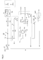
- FIG. 2 is a block diagram which shows a configuration of a driver/comparator circuit 100 according to an embodiment.
- the driver/comparator circuit 100 is an interface circuit for a first device.
- the driver/comparator circuit 100 is connected to a communication partner device (which will be referred to as the “second device” hereafter) 102 via a transmission line 104 , and outputs a signal Vd′ to the second device 102 , or receives a signal Vu output from the second device 102 .
- the driver/comparator circuit 100 is suitably employed as an interface circuit for automatic test equipment ATE (Automatic Test Equipment) (which is also referred to as “pin electronics”). That is to say, the driver/comparator circuit 100 outputs pattern data to the second device (DUT). At the same time, the driver/comparator circuit 100 receives a signal from the DUT, and judges the amplitude (level) of the signal thus received.
- ATE Automatic Test Equipment
- FIG. 2 Such a case of a test system is shown in FIG. 2 .
- the second device 102 includes a driver amplifier DRV 2 and an output resistor Ru.
- the signal Vu output from the driver amplifier DRV 2 is input to an input/output terminal P 1 of the driver/comparator circuit 100 via the transmission line 104 .
- the output resistor Ru is provided to the driver amplifier DRV 2 . Description will be made below under the assumption that impedance matching is achieved between the characteristic impedance Z 0 of the transmission line 104 and the output resistor Ru included in the second device 102 .
- the driver/comparator circuit 100 includes the input/output terminal P 1 via which the transmission line 104 is connected.
- the driver/comparator circuit 100 includes a comparison judgment circuit 10 , a driver amplifier DRV 1 , and a third resistor R 3 .
- the driver amplifier DRV 1 generates a signal Vd′ which is to be transmitted to the second device 102 .
- the signal Vd′ may be transmitted in the form of a binary signal which may be either high or low, or may be transmitted in the form of a multi-valued signal such as a four-valued signal or an eight-valued signal.
- the third resistor R 3 is provided between the output terminal of the driver amplifier DRV 1 and the input/output terminal P 1 .
- the driver amplifier DRV 1 may generate a constant voltage.
- the comparison judgment circuit 10 judges the amplitude level of the voltage Va′ that occurs at the input/output terminal P 1 .
- the comparison judgment circuit 10 includes an attenuator circuit 12 , a protection circuit 20 , and a level comparator CMP 1 .
- the attenuator circuit 12 attenuates the voltage Va′ at the input/output terminal P 1 so as to generate an attenuated voltage Vc.
- the level comparator CMP 1 compares the attenuated voltage Vc thus generated with a predetermined upper threshold voltage VOH′, and generates a level judgment signal SH that corresponds to the comparison result.
- the comparison judgment circuit 10 may further includes a comparator (not shown) arranged in parallel with the level comparator CMP 1 , and configured to compare the attenuated voltage Vc with a predetermined lower threshold voltage VOL′.
- the attenuated voltage Vc is supplied to the level comparator CMP 1 via the protection circuit 20 .
- the protection circuit 20 forcibly cuts off the attenuated voltage Vc to be supplied to the level comparator CMP 1 , or changes the voltage value thereof.
- the driver/comparator circuit 100 The above is the configuration of the driver/comparator circuit 100 . Next, description will be made regarding the operation thereof.
- the driver/comparator circuit 100 shown in FIG. 2 the voltage Va′ at the input/output terminal P 1 is attenuated by the attenuator circuit 12 .
- the signal Vc having a small amplitude is input to the level comparator CMP 1 even in a case in which the second device 102 generates the voltage Vu having a large amplitude.
- the level comparator CMP 1 can be configured using a low breakdown voltage device, thereby providing high-speed comparison processing. That is to say, such an arrangement is capable of appropriately evaluating the voltage level of a high-speed signal.
- the protection circuit 20 protects the level comparator CMP 1 from such an overvoltage state.
- the level comparator CMP 1 giving consideration not only to the output voltage of the second device 102 in the normal state, but also to abnormal states such as short-circuits to the power supply or the ground, surge noise, etc.
- the driver/comparator circuit 100 by providing the protection circuit 20 , the level comparator CMP 1 is not exposed to an overvoltage state in such an abnormal state, thereby enabling the design of a lower breakdown voltage of the level comparator CMP 1 . Together with the attenuator circuit 12 thus provided, this improves performance of the high-speed operation of the driver/comparator circuit 100 .
- FIG. 3 is a circuit diagram which shows a specific first example configuration of the comparison judgment circuit 10 shown in FIG. 2 .
- the attenuator circuit 12 includes a first resistor R 1 , a second resistor R 2 , and a first voltage source VS 1 .
- a first terminal of the first resistor R 1 is connected to the input/output terminal P 1 .
- a first terminal of the second resistor R 2 is connected to a second terminal of the first resistor R 1 .
- a first voltage Vs is applied to a second terminal of the second resistor R 2 .
- the first voltage Vs is generated by the first voltage source VS 1 .
- the attenuator circuit 12 outputs, as the attenuated voltage Vc, the electric potential at a connection node that connects the first resistor R 1 and the second resistor R 2 .
- the resistance value of the first resistor R 1 will be represented by Rb, and the resistance value of the second resistor R 2 will be represented by Rc.
- the resistance values of the first resistor R 1 and the second resistor R 2 can be determined as desired.
- Vc ( Rc ⁇ Va′+Rb ⁇ Vs )/( Rb+Rc )
- the attenuator circuit 12 attenuates the amplitude, i.e., the change in the voltage Va′ at the input/output terminal P 1 , with an attenuation factor of Rc/(Rb+Rc). Furthermore, the attenuator circuit 12 applies a level shift that corresponds to the first voltage Vs. In a case in which the first voltage Vs is the ground voltage (0 V), the shift amount is zero. Description will be made later regarding the effects of the level shift operation.
- the protection circuit 20 shown in FIG. 3 includes a voltage monitoring circuit 22 and a protection switch SW 1 .
- the voltage monitoring circuit 22 generates a protection signal NOV which is asserted (set to the low level) when the attenuated voltage Vc deviates from a predetermined voltage range (VCmin to VCmax).
- the voltage monitoring circuit 22 includes an upper-limit comparator 24 , a lower-limit comparator 26 , a first flip-flop 28 , a second flip-flop 30 , and a NOR gate 32 .
- the upper-limit comparator 24 compares the attenuated voltage Vc with a maximum voltage VCmax, and generates a first detection signal PCH which indicates the comparison result.
- the lower-limit comparator 26 compares the attenuated voltage Vc with a minimum voltage VCmin, and generates a second detection signal PCL which indicates the comparison result.
- the maximum voltage VCmax is set to the maximum voltage value at which the level comparator CMP 1 that receives such a voltage as an input signal can operate without any difficulty (without causing any stress).
- the minimum voltage VCmin is set to the minimum voltage value at which the level comparator CMP 1 that receives such a voltage as an input can operate without any difficulty.
- the first detection signal PCH is set to the high level.
- Vc ⁇ VCmin the second detection signal PCL is set to the high level. That is to say, when the attenuated voltage Vc deviates from the voltage range VCmin to VCmax, one of the signals PCH or PCL is set to the high level.
- the signals PCH and PCL are input to the set terminals (S) of the first flip-flop 28 and the second flip-flop 30 , respectively.
- Each of the flip-flops 28 and 30 receives a reset signal from an external circuit via the reset terminal (R) thereof.
- the NOR gate 32 generates the logical NOR of the output signals of the first flip-flop 28 and the second flip-flop 30 . That is to say, when the attenuated voltage Vc is within the input voltage range defined by the level comparator CMP 1 , the protection signal NOV generated by the NOR gate 32 is high level (negated). When the attenuated voltage Vc deviates from the input voltage range, the protection signal NOV is low level (asserted).
- the protection switch SW 1 is provided on a path from the attenuator circuit 12 to the level comparator CMP 1 .
- a high-level signal is input, i.e., when the protection signal NOV is negated, the protection switch SW 1 is set to the conducting state, and when a low-level signal is input, i.e., when the production signal NOV is asserted, the protection switch SW 1 is set to the cutoff state.
- the design approach is to make the characteristics of the driver/comparator circuit 100 shown in FIG. 3 match the characteristics of the typical driver/comparator circuit 400 shown in FIG. 1 .
- the design approach is to provide functions equivalent to those of the typical driver/comparator circuit 400 , which does not include the attenuator circuit 12 , to the driver/comparator circuit 100 including the attenuator circuit 12 .
- the output voltage Vd′ (Vd) of the driver amplifier DRV 1 can exhibit various electric potential values such as a high-level value (VIH), low-level value (VIL), a terminal electric potential value (VT), or the like, depending on the data to be transmitted to the second device 102 .
- VH high-level value
- VIL low-level value
- VT terminal electric potential value
- description will be made regarding a simple arrangement in which the output voltage Vd′ (Vd) is set to a fixed electric potential.
- FIGS. 4A and 4B are circuit diagrams obtained by excerpting only the circuit components that relate to the impedance from, respectively, the driver/comparator circuit 400 shown in FIG. 1 and the driver/comparator circuit 100 shown in FIG. 3 . From Thevenin's theorem, in order for these two circuits to be equivalent, the following first requirement and second requirement must be satisfied.
- the first requirement is that the internal impedance Z 1 of the driver/comparator circuit 100 shown in FIG. 3 measured via the input/output terminal P 1 thereof be equal to the internal impedance Z 2 of the driver/comparator circuit 400 shown in FIG. 1 measured via the input/output terminal P 1 thereof.
- the second requirement is that the voltage level of the signal Va′ output from the input/output terminal P 1 of the driver/comparator circuit 100 shown in FIG. 3 be equal to the voltage level of the signal Va output from the input/output terminal P 1 of the driver/comparator circuit 400 shown in FIG. 1 .
- Expression (3) is obtained by transforming Expression (1). Furthermore, Expression (4) is obtained with reference to FIG. 4B . Expression (2) is applied to Expression (4), thereby obtaining Expression (5).
- Ra ′ Ra ⁇ ( Rb + Rc ) Rb + Rc - Ra ( 3 )
- Va ′ Vd ′ ⁇ ( Rb + Rc ) + Vs ⁇ Ra ′ Ra ′ + Rb + Rc ( 4 )
- Vd Vd ′ ⁇ ( Rb + Rc ) + Vs ⁇ Ra ′ Ra ′ + Rb + Rc ( 5 )
- Expression (6) is obtained by transforming Expression (5). If an output voltage Vd′ that satisfies Expression (6) is chosen for the driver amplifier DRV 1 , the driver/comparator circuit 100 shown in FIG. 3 is equivalent to the driver/comparator circuit 400 shown in FIG. 1 .
- Vd ′ Vd ⁇ ( Ra ′ + Rb + Rc ) Rb + Rc - Vs ⁇ Ra ′ Rb + Rc ( 6 )
- FIGS. 5A and 5B are circuit diagrams obtained by excerpting only the circuit components that relate to the voltage comparison performed by, respectively, the driver/comparator circuit 400 shown in FIG. 1 and the driver/comparator circuit 100 shown in FIG. 3 .
- the Expression (7) is obtained with reference to FIG. 5B .
- Vc Vs ⁇ Rb + Va ⁇ Rc Rb + Rc ( 7 )
- VOH ′ Vs ⁇ Rb + VOH ⁇ Rc Rb + Rc ( 10 )
- Vd′, Ra′, and VOH′ should be chosen such that Expression (6) and Expression (10) are satisfied.
- a reset signal RST is asserted, and the output signals OVH and OVL of the first flip-flop 28 and the second flip-flop 30 are each set to the low level.
- the protection signal NOV is set to the high level (is negated), which sets the protection switch SW 1 to the on (conducting) state.
- the signals PCH, PCL, OVH, and OVL are each set to the low level. Accordingly, the protection signal NOV remains at the high level.
- the signal PCH When the input voltage Vc satisfies the relation Vc>VCmax, the signal PCH is set to the high level, which sets the first flip-flop 28 , thereby setting OVH to the high level.
- the protection signal NOV is set to the low level (is asserted), which sets the protection switch SW 1 to the off state. After the protection signal NOV is asserted, the protection switch SW 1 remains in this state until the next reset signal RST is asserted.
- the signal PCL When the input voltage Vc satisfies the relation Vc ⁇ VCmin, the signal PCL is set to the high level, which sets the second flip-flop 30 , thereby setting OVL to the high level.
- the protection signal NOV Upon receiving OVL thus switched to the high level, the protection signal NOV is set to the low level (is asserted), which sets the protection switch SW 1 to the off state. In the same way as described above, after the protection signal NOV is asserted, the protection switch SW 1 remains in this state until the next reset signal RST is asserted.
- the driver/comparator circuit 100 shown in FIG. 3 is capable of suitably limiting the input voltage Vc of the level comparator CMP 1 .
- the attenuator circuit 12 is capable of shifting the input voltage (attenuated voltage) Vc of the level comparator CMP 1 according to the first voltage Vs.
- Vc input voltage
- Vs first voltage
- FIG. 6 is a circuit diagram which shows a configuration of a driver/comparator circuit 100 a according to a first modification.
- the voltage monitoring circuit 22 of a comparison judgment circuit 10 a monitors the electric potential Va′ at the input/output terminal P 1 , instead of the input voltage (attenuated voltage) Vc of the level comparator CMP 1 .
- the other configuration is the same as that shown in FIG. 3 .
- the Expression (7) is transformed, thereby obtaining the Expression (6-1).
- the allowable input voltage range for the level comparator CMP 1 is between VCmin and VCmax. Accordingly, Vc in the Expression (6-1) is replaced with VCmax and VCmin, thereby obtaining the Expression (6-2).
- Va Vc ⁇ ( Rb + Rc ) - Vs ⁇ Rb Rc ( 6 ⁇ - ⁇ 1 )
- VA ⁇ ⁇ max VC ⁇ max ⁇ ( Rb + Rc ) - Vs ⁇ Rb Rc ( 6 ⁇ - ⁇ 2 )
- VA ⁇ ⁇ min VC ⁇ min ⁇ ( Rb + Rc ) - Vs ⁇ Rb Rc
- the voltage monitoring circuit 22 is connected to a node having a low impedance (e.g., 50 ⁇ ).
- a low impedance e.g. 50 ⁇
- FIG. 7 is a circuit diagram which shows a comparison judgment circuit 10 b included in a driver/comparator circuit according to a second embodiment.
- a dynamic comparator is employed as the level comparator CMP 1 .
- the level comparator CMP 1 judges, and latches, the amplitude level of the input voltage Vc at a timing set according to a control signal ( ⁇ 3 ).
- the level comparator CMP 1 includes an input hold unit 110 , a comparison amplifier unit 120 , a reset unit 130 , and a first capacitor C 1 through a fourth capacitor C 4 .
- the input voltage Vc is input to the positive-side input terminal TP, and the threshold voltage VOH′ is input to the negative-side input terminal TN.
- the power supply voltage Vdd is supplied as a first fixed voltage to a power supply terminal (first fixed voltage terminal) 50 .
- the ground voltage VGND is supplied as a second fixed voltage to a ground terminal (second fixed voltage terminal) 52 .
- a positive-side differential signal IP (signal HP held by the input hold unit 110 ) propagates through a positive-side line LP.
- a negative-side differential signal IN (signal HN held by the input hold unit 110 ) propagates through a negative-side line LN.
- the comparison amplifier unit 120 includes a first inverter 122 , a second inverter 124 , and an activating switch 126 .
- the comparison amplifier unit 120 has a configuration which is referred to as a “dynamic comparator”, a “sense latch”, or the like.
- the input terminal of the first inverter 122 is connected to the positive-side output line OP, and the output terminal thereof is connected to the negative-side output line ON.
- the first inverter 122 includes transistors PMOS, NOMS 1 , and NMOS 2 .
- the first inverter 122 inverts and amplifies the signal input to the gate of the transistor NMOS 1 , and outputs the signal thus inverted and amplified via the drain of the transistor NMOS 1 (drain of the PMOS).
- the gates of the transistors PMOS and NMOS 2 are connected so as to form a common gate electrode, which is connected to the output terminal of the second inverter 124 .
- the second inverter 124 has the same configuration as that of the first inverter 122 .
- the first inverter 122 and the second inverter 124 are cross-coupled.
- the input terminal of the second inverter 124 is connected to the negative-side output line ON, and the output terminal thereof is connected to the positive-side output line OP.
- One of the power supply terminals of the second inverter 124 (the PMOS source terminal) is connected to a power supply terminal (first fixed voltage terminal) 50 , and the other power supply terminal thereof (the NMOS 2 source terminal) is connected to the power supply terminal of the first inverter 122 (the NMOS 2 source terminal) so as to form a common power supply electrode.
- each of the inverters 122 and 124 may be configured as a CMOS inverter formed of a NMOS transistor and a PMOS transistor connected in series.
- the activating switch 126 is arranged such that a power supply voltage (first fixed voltage) Vdd or the ground voltage (second fixed voltage) VGND is applied to the common power supply terminal formed by connecting the other power supply terminals (the NMOS 2 source terminals) of the first inverter 122 and the second inverter 124 .
- a third control signal ⁇ 3 is input to the input terminal of the activating switch 126 .
- the output voltage of the activating switch 126 is set to the first fixed voltage (power supply voltage Vdd), which inactivates the first inverter 122 and the second inverter 124 .
- the output voltage of the activating switch 126 is set to the second fixed voltage (ground voltage VGND), which activates the first inverter 122 and the second inverter 124 .
- the first capacitor C 1 and the second capacitor C 2 are connected to the positive-side output line OP and the negative-side output line ON, respectively.
- the first capacitor C 1 and the second capacitor C 2 may each be explicitly formed by provision of a MIM (Metal-Insulator-Metal) capacitance.
- a parasitic capacitance gate capacitance of the transistor or wiring capacitance
- FIG. 7 shows an arrangement in which the first capacitor C 1 and the second capacitor C 2 are provided between the positive-side output line OP and the ground, and between the negative-side output line ON and the ground, respectively.
- the positive-side output line OP and the negative-side output line ON may be coupled via a single capacitor.
- the input hold unit 110 is arranged as an upstream component of the comparison amplifier unit 120 .
- the input hold unit 110 has a function for electrically disconnecting a node that connects the input terminal of the comparison amplifier unit 120 and the positive-side input terminal TP and a node that connects the input terminal of the comparison amplifier unit 120 and the negative-side input terminal TN.
- the input hold unit 110 holds a differential signal IP/IN at a timing according to an instruction defined by the first control signal ⁇ 1 .
- the input hold unit 110 outputs the differential signal HN/HP thus held to the comparison amplifier unit 120 , which is arranged as a downstream component, at a timing according to an instruction defined by the second control signal ⁇ 2 .
- the input hold unit 110 includes a first positive-side switch SW 1 p , a second positive-side switch SW 2 p, a first negative-side switch SW 1 n , a second negative-side switch SW 2 n , a third capacitor C 3 , and a fourth capacitor C 4 .
- the first positive-switch SW 1 p and the second positive-side switch SW 2 p are arranged in series between the positive-side input terminal TP and the positive-side line LP.
- a path that connects the first positive-side switch SW 1 p and the second positive-side switch SW 2 p is coupled to the ground via the third capacitor C 3 .
- the electric potential at the third capacitor C 3 (positive-side hold signal HP) is determined according to the positive-side differential signal IP.
- the control signal ⁇ 1 is negated (switched to the low level) at a certain timing
- the first positive-side switch SW 1 p is turned off, and the third capacitor C 3 holds the positive-side differential signal IP at this timing.
- the second control signal ⁇ 2 is asserted so as to turn on the second positive-side switch SW 2 p , the positive-side hold signal HP thus held is supplied to the positive-side line LP.
- the first negative switch SW 1 n , the second negative-side switch SW 2 n , and the fourth capacitor C 4 are connected in the same way. Such an arrangement holds the negative-side differential signal IN.
- the third capacitor C 3 and the fourth capacitor C 4 may each be configured as a MIN capacitance or a parasitic capacitance, in the same way as the first capacitor C 1 and the second capacitor C 2 . Also, instead of providing the third capacitor C 3 and the fourth capacitor C 4 , the line on which the positive-side hold signal HP occurs and the line on which the negative-side hold signal HN occurs may be coupled via a single capacitor.
- the reset unit 130 is provided in order to initialize the positive-side output signal OP and the negative-side output signal ON to the first fixed voltage (power supply voltage Vdd).
- the reset unit 130 includes a first reset switch SWr 1 and a second reset switch SWr 2 .
- the first reset switch SWr 1 is provided between the positive-side output line OP and the power supply terminal 50 (first fixed voltage terminal).
- the second reset switch SWr 2 is provided between the negative-side output line ON and the power supply terminal 50 .
- the positive-side output signal OP and the negative-side output signal ON are weakly pulled up by the power supply voltage Vdd due to a transistor which is a component of the comparison amplifier unit 120 , even when the first reset switch SWr 1 and the second reset switch SWr 2 are not on.
- the reset unit 130 may be eliminated.
- the AND gate 34 generates the logical AND of the first control signal ⁇ 1 and the protection signal NOV.
- the first switches SW 1 p and SW 1 n are controlled according to the output signal of the AND gate 34 .
- the first switches SW 1 p and SW 1 n correspond to the protection switch SW 1 shown in FIG. 3 .
- the level comparator CMP 1 shown in FIG. 7 may have a configuration in which the power supply voltage and the ground voltage are reversed, which is effective as an embodiment.
- FIG. 8 is a circuit diagram which shows a configuration of a driver/comparator circuit 100 c according to a third embodiment.
- the comparison judgment circuit 10 shown in FIG. 3 protects the level comparator CMP 1 by cutting off the input voltage Vc of the level comparator CMP 1 in the overvoltage state.
- the comparison judgment circuit 10 c according to the third modification protects the level comparator CMP 1 by level-shifting the input voltage Vc in the overvoltage state.
- An attenuator circuit 12 c shown in FIG. 8 further includes a second voltage source VS 2 , a third voltage source VS 3 , and a first switch SW 11 to a third switch SW 13 , in addition to the components of the attenuator circuit 12 shown in FIG. 3 .
- the first voltage source VS 1 to the third voltage source VS 3 generate voltages VCT, VPH, and VPL, respectively. These voltages satisfy the following relation expression. VPH ⁇ VCT ⁇ VPL
- One switch selected from the first switch SW 11 to the third switch SW 13 is turned on according to the monitoring result obtained by a voltage monitoring circuit 22 c.
- a block including the voltage sources VS 1 to VS 3 and the switches SW 11 to SW 13 can be regarded as a variable voltage source 40 . Also, any arrangement may be made which is capable of switching the voltage to be applied to the second terminal of the second resistor R 2 .
- the voltage monitoring circuit 22 c further includes OR gates 36 and 38 , in addition to the components of the voltage monitoring circuit 22 shown in FIG. 3 .
- PCL When PCL is asserted, the first flip-flop 28 is reset.
- PCH When PCH is asserted, the second flip-flop 30 is reset.
- Vc is greater than VCmax
- PCH is asserted, which turns on the second switch SW 12 , and turns off the first switch SW 11 .
- Vs is set to VPH.
- the input voltage Vc of the level comparator CMP 1 is shifted to the low-voltage side according to Expression (7).
- the value of VPH is determined such that the input voltage Vc′ thus shifted satisfies the relation Vc′ ⁇ VCmax.
- Vc is less than VCmin
- PCL is asserted, which turns on the third switch SW 13 , and turns off the first switch SW 11 .
- Vs is set to VPL, and the input voltage Vc of the level comparator CMP 1 is shifted to the high-voltage side according to Expression (7).
- the value of VPL is determined such that the input voltage Vc′ thus shifted satisfies the relation Vc′>VCmin.
- FIG. 9 is a circuit diagram which shows another configuration of the variable voltage source 40 shown in FIG. 8 .
- the registers (latches) 42 , 44 , and 46 hold L-bit (L is an integer) digital data DCT, DPH, and DPL that correspond to the voltages VCT, VPH, and VPL, respectively.
- the signals NOV, OVH, and OVL are asserted in a complementary manner.
- one of the control data DCT, DPH, and DPL is input to an R-2R termination circuit 60 .
- the R-2R termination circuit 60 includes an (L+1)-stage R-2R network and (L+1) buffers each of which is arranged to apply voltage to one terminal of the resistor R of the corresponding stage.
- the higher order L bits of the digital data are assigned to the respective buffers in order of how close they are to the output terminal.
- a fixed electric potential e.g., ground potential
- variable voltage source 40 can be regarded as a voltage source having an output impedance Rc, which is equivalent to the variable voltage source 40 shown in FIG. 8 .
- variable voltage source 40 With the variable voltage source 40 shown in FIG. 9 , the voltages VCT, VPH, and VPL are suitably controlled according to the bit values of the digital data DCT, DPH, and DPL.
- FIG. 10 is a block diagram which shows a configuration of a driver/comparator circuit 100 d according to a fourth modification.
- the input/output terminal P 1 is connected to N (N is an integer of 2 or more) comparison judgment circuits 10 _ 1 to 10 _N in parallel.
- the resistance value of the first resistor R 1 is preferably set to N ⁇ Rb
- the resistance value of the second resistor R 2 is preferably set to N ⁇ Rc.
- the aforementioned Expression (3) can be applied without change.
- VOHi ′ Vsi ⁇ Rb + VOHi ⁇ Rc ⁇ Rb + Rc ( 10 ′ )
- VA ⁇ ⁇ i ⁇ ⁇ max VC ⁇ max ⁇ ( Rb + Rc ) - Vsi ⁇ Rb Rc
- VAi ⁇ ⁇ min VC ⁇ min ⁇ ( Rb + Rc ) - Vsi ⁇ Rb Rc ⁇ ( 6 ⁇ - ⁇ 2 ′ )
- the amplitude of the signal output from the second device 102 can be compared with multiple different threshold voltages.
Landscapes
- Physics & Mathematics (AREA)
- General Physics & Mathematics (AREA)
- Engineering & Computer Science (AREA)
- Power Engineering (AREA)
- General Engineering & Computer Science (AREA)
- Logic Circuits (AREA)
- Tests Of Electronic Circuits (AREA)
Abstract
Description
- [Patent Document 1]
- [Patent Document 2]
- [Patent Document 3]
- [Patent Document 4]
Vc=(Rc·Va′+Rb·Vs)/(Rb+Rc)
Ra=Ra′//(Rb+Rc) (1)
Va′=Va=Vd (2)
A//B=A×B/(A+B)
SH=Lo (when Va>VOH)
SH=Hi (when Va<VOH) (8)
SH′=Lo (when Vc>VOH′)
SH′=Hi (when Vc<VOH′) (9)
VPH<VCT<VPL
Claims (9)
Applications Claiming Priority (1)
| Application Number | Priority Date | Filing Date | Title |
|---|---|---|---|
| PCT/JP2009/002473 WO2010140190A1 (en) | 2009-06-02 | 2009-06-02 | Comparative decision circuit and test device using same |
Publications (2)
| Publication Number | Publication Date |
|---|---|
| US20110121904A1 US20110121904A1 (en) | 2011-05-26 |
| US8704527B2 true US8704527B2 (en) | 2014-04-22 |
Family
ID=43297338
Family Applications (1)
| Application Number | Title | Priority Date | Filing Date |
|---|---|---|---|
| US12/745,889 Active 2031-04-03 US8704527B2 (en) | 2009-06-02 | 2009-06-02 | Comparison judgment circuit |
Country Status (3)
| Country | Link |
|---|---|
| US (1) | US8704527B2 (en) |
| JP (1) | JPWO2010140190A1 (en) |
| WO (1) | WO2010140190A1 (en) |
Families Citing this family (5)
| Publication number | Priority date | Publication date | Assignee | Title |
|---|---|---|---|---|
| US10359452B2 (en) | 2012-07-11 | 2019-07-23 | Hewlett-Packard Development Company, L.P. | Diagnostic device, apparatus and method |
| WO2016173619A1 (en) * | 2015-04-27 | 2016-11-03 | Advantest Corporation | Switch circuit, method for operating a switch circuit and an automated test equipment |
| JP2017181574A (en) | 2016-03-28 | 2017-10-05 | 株式会社ジャパンディスプレイ | Display device |
| US10862521B1 (en) * | 2019-01-30 | 2020-12-08 | Inphi Corporation | Techniques for programmable gain attenuation in wideband matching networks with enhanced bandwidth |
| TWI847231B (en) * | 2021-10-01 | 2024-07-01 | 致茂電子股份有限公司 | Wafer inspection method and inspection equipment |
Citations (13)
| Publication number | Priority date | Publication date | Assignee | Title |
|---|---|---|---|---|
| JPH04251517A (en) | 1990-12-28 | 1992-09-07 | Yokogawa Electric Corp | Overvoltage protection circuit |
| JPH05312899A (en) | 1992-05-06 | 1993-11-26 | Advantest Corp | Liquid crystal driver ic test device |
| US5440441A (en) * | 1984-10-24 | 1995-08-08 | Ahuja; Om | Apparatus for protecting, monitoring, and managing an AC/DC electrical line or a telecommunication line using a microprocessor |
| JPH08327705A (en) | 1995-03-31 | 1996-12-13 | Toshiba Microelectron Corp | Comparator circuit |
| JPH1010200A (en) | 1996-06-26 | 1998-01-16 | Hitachi Ltd | Semiconductor device testing method and semiconductor testing device |
| JPH10232266A (en) | 1997-02-20 | 1998-09-02 | Advantest Corp | Semiconductor test device |
| JPH10240560A (en) | 1997-02-26 | 1998-09-11 | Toshiba Corp | Waveform signal processing device |
| JPH11237438A (en) | 1998-02-20 | 1999-08-31 | Advantest Corp | Semiconductor testing device |
| US6232815B1 (en) | 1999-05-06 | 2001-05-15 | Analog Devices, Inc. | ATE pin electronics with complementary waveform drivers |
| US20030057990A1 (en) * | 2001-08-17 | 2003-03-27 | West Burnell G. | Pin electronics interface circuit |
| JP2006194664A (en) | 2005-01-12 | 2006-07-27 | Nippon Seiki Co Ltd | Measuring meter for vehicle |
| JP2006194644A (en) | 2005-01-11 | 2006-07-27 | Advantest Corp | Signal transmission system, signal output circuit board, signal receiving circuit board, signal output method and signal receiving method |
| US20060273811A1 (en) * | 2005-05-19 | 2006-12-07 | Geoffrey Haigh | Using an active load as a high current output stage of a precision pin measurement unit in automatic test equipment systems |
-
2009
- 2009-06-02 WO PCT/JP2009/002473 patent/WO2010140190A1/en not_active Ceased
- 2009-06-02 JP JP2010513529A patent/JPWO2010140190A1/en not_active Withdrawn
- 2009-06-02 US US12/745,889 patent/US8704527B2/en active Active
Patent Citations (13)
| Publication number | Priority date | Publication date | Assignee | Title |
|---|---|---|---|---|
| US5440441A (en) * | 1984-10-24 | 1995-08-08 | Ahuja; Om | Apparatus for protecting, monitoring, and managing an AC/DC electrical line or a telecommunication line using a microprocessor |
| JPH04251517A (en) | 1990-12-28 | 1992-09-07 | Yokogawa Electric Corp | Overvoltage protection circuit |
| JPH05312899A (en) | 1992-05-06 | 1993-11-26 | Advantest Corp | Liquid crystal driver ic test device |
| JPH08327705A (en) | 1995-03-31 | 1996-12-13 | Toshiba Microelectron Corp | Comparator circuit |
| JPH1010200A (en) | 1996-06-26 | 1998-01-16 | Hitachi Ltd | Semiconductor device testing method and semiconductor testing device |
| JPH10232266A (en) | 1997-02-20 | 1998-09-02 | Advantest Corp | Semiconductor test device |
| JPH10240560A (en) | 1997-02-26 | 1998-09-11 | Toshiba Corp | Waveform signal processing device |
| JPH11237438A (en) | 1998-02-20 | 1999-08-31 | Advantest Corp | Semiconductor testing device |
| US6232815B1 (en) | 1999-05-06 | 2001-05-15 | Analog Devices, Inc. | ATE pin electronics with complementary waveform drivers |
| US20030057990A1 (en) * | 2001-08-17 | 2003-03-27 | West Burnell G. | Pin electronics interface circuit |
| JP2006194644A (en) | 2005-01-11 | 2006-07-27 | Advantest Corp | Signal transmission system, signal output circuit board, signal receiving circuit board, signal output method and signal receiving method |
| JP2006194664A (en) | 2005-01-12 | 2006-07-27 | Nippon Seiki Co Ltd | Measuring meter for vehicle |
| US20060273811A1 (en) * | 2005-05-19 | 2006-12-07 | Geoffrey Haigh | Using an active load as a high current output stage of a precision pin measurement unit in automatic test equipment systems |
Non-Patent Citations (5)
| Title |
|---|
| IPRP for corresponding PCT/JP2009/002473 issued on Dec. 12, 2011. |
| Office action for related Japanese patent application No. 2010-513529 issued on May 21, 2013 and an English translation. |
| PCT International Search Report for PCT Application No. PCT/JP2009/002473 mailed on Sep. 8, 2009. |
| PCT Written Opinion for PCT Application No. PCT/JP2009/002473 mailed on Sep. 8, 2009. |
| WO for corresponding PCT/JP2009/002473 mailed on Sep. 8, 2009, along with its English translation. |
Also Published As
| Publication number | Publication date |
|---|---|
| WO2010140190A1 (en) | 2010-12-09 |
| US20110121904A1 (en) | 2011-05-26 |
| JPWO2010140190A1 (en) | 2012-11-15 |
Similar Documents
| Publication | Publication Date | Title |
|---|---|---|
| US8030965B2 (en) | Level shifter using SR-flip flop | |
| US7617064B2 (en) | Self-test circuit for high-definition multimedia interface integrated circuits | |
| US8704527B2 (en) | Comparison judgment circuit | |
| CN101231626A (en) | Interface circuits and semiconductor integrated circuits | |
| US7729097B2 (en) | Over-voltage and under voltage protection circuit | |
| US20100264970A1 (en) | Edge rate control for i2c bus applications | |
| US7873922B2 (en) | Structure for robust cable connectivity test receiver for high-speed data receiver | |
| US7855563B2 (en) | Robust cable connectivity test receiver for high-speed data receiver | |
| US20120043968A1 (en) | Variable equalizer circuit | |
| US7852119B1 (en) | SR-flip flop with level shift function | |
| EP4350371A1 (en) | Very low voltage i/o circuit and method for screening defects | |
| EP3474027B1 (en) | Method for identifying a fault at a device output and system therefor | |
| US11313904B2 (en) | Testing device and testing method | |
| US7679390B2 (en) | Test apparatus and pin electronics card | |
| US8183893B2 (en) | Driver comparator circuit | |
| US8324928B2 (en) | Calibration circuit | |
| US6275055B1 (en) | Semiconductor integrated circuit | |
| US7157931B2 (en) | Termination circuits having pull-down and pull-up circuits and related methods | |
| JP4944793B2 (en) | Test equipment and pin electronics card | |
| CN113615089A (en) | Switching device for converting differential input signals and system having a switching device | |
| US6681355B1 (en) | Analog boundary scan compliant integrated circuit system | |
| US20080150608A1 (en) | Integrated semiconductor circuit | |
| US9172362B2 (en) | Multifunction word recognizer element | |
| US20260019066A1 (en) | Glitch-free power supply independent sequence circuit | |
| US12244331B2 (en) | Differential input receiver circuit testing with a loopback circuit |
Legal Events
| Date | Code | Title | Description |
|---|---|---|---|
| AS | Assignment |
Owner name: ADVANTEST CORPORATION, JAPAN Free format text: ASSIGNMENT OF ASSIGNORS INTEREST;ASSIGNOR:KOJIMA, SHOJI;REEL/FRAME:024476/0042 Effective date: 20100524 |
|
| AS | Assignment |
Owner name: ADVANTEST CORPORATION, JAPAN Free format text: ASSIGNMENT OF ASSIGNORS INTEREST;ASSIGNOR:KOJIMA, SHOJI;REEL/FRAME:025188/0699 Effective date: 20100524 |
|
| STCF | Information on status: patent grant |
Free format text: PATENTED CASE |
|
| MAFP | Maintenance fee payment |
Free format text: PAYMENT OF MAINTENANCE FEE, 4TH YEAR, LARGE ENTITY (ORIGINAL EVENT CODE: M1551) Year of fee payment: 4 |
|
| AS | Assignment |
Owner name: ADVANTEST CORPORATION, JAPAN Free format text: CHANGE OF ADDRESS;ASSIGNOR:ADVANTEST CORPORATION;REEL/FRAME:047987/0626 Effective date: 20181112 |
|
| MAFP | Maintenance fee payment |
Free format text: PAYMENT OF MAINTENANCE FEE, 8TH YEAR, LARGE ENTITY (ORIGINAL EVENT CODE: M1552); ENTITY STATUS OF PATENT OWNER: LARGE ENTITY Year of fee payment: 8 |
|
| MAFP | Maintenance fee payment |
Free format text: PAYMENT OF MAINTENANCE FEE, 12TH YEAR, LARGE ENTITY (ORIGINAL EVENT CODE: M1553); ENTITY STATUS OF PATENT OWNER: LARGE ENTITY Year of fee payment: 12 |