US8645444B2 - IIR filter for reducing the complexity of multiplying elements - Google Patents
IIR filter for reducing the complexity of multiplying elements Download PDFInfo
- Publication number
- US8645444B2 US8645444B2 US12/745,726 US74572608A US8645444B2 US 8645444 B2 US8645444 B2 US 8645444B2 US 74572608 A US74572608 A US 74572608A US 8645444 B2 US8645444 B2 US 8645444B2
- Authority
- US
- United States
- Prior art keywords
- signal
- filtered signal
- filter
- sub
- unit
- Prior art date
- Legal status (The legal status is an assumption and is not a legal conclusion. Google has not performed a legal analysis and makes no representation as to the accuracy of the status listed.)
- Expired - Fee Related, expires
Links
Images


Classifications
-
- H—ELECTRICITY
- H03—ELECTRONIC CIRCUITRY
- H03H—IMPEDANCE NETWORKS, e.g. RESONANT CIRCUITS; RESONATORS
- H03H17/00—Networks using digital techniques
- H03H17/02—Frequency selective networks
- H03H17/0223—Computation saving measures; Accelerating measures
-
- H—ELECTRICITY
- H03—ELECTRONIC CIRCUITRY
- H03H—IMPEDANCE NETWORKS, e.g. RESONANT CIRCUITS; RESONATORS
- H03H17/00—Networks using digital techniques
- H03H17/02—Frequency selective networks
- H03H17/0223—Computation saving measures; Accelerating measures
- H03H17/0227—Measures concerning the coefficients
-
- H—ELECTRICITY
- H03—ELECTRONIC CIRCUITRY
- H03H—IMPEDANCE NETWORKS, e.g. RESONANT CIRCUITS; RESONATORS
- H03H17/00—Networks using digital techniques
- H03H17/02—Frequency selective networks
- H03H17/04—Recursive filters
Definitions
- the present invention relates to IIR filters, and in particular to a method and an architecture for reducing the complexity of multiplying elements in such filters.
- IIR Infinite Impulse Response
- the signals are intentionally highly over-sampled, meaning that the ratio of the sample rate to highest signal frequency component is high. Although this may at first seem to be inefficient, this does allow a reduction in the number of bits used to represent the signal, and this is often the reason for using over-sampling. For example, it is sometimes appropriate to use only one bit to represent the signal at the over-sampled rate.
- an ambient noise cancellation system One such example is an ambient noise cancellation system.
- IIR filter There are several standard implementations of the IIR filter, for example the so-called “Direct Form I” and “Direct Form II” types. It is also common to split a higher-order filter into parallel or cascaded second-order sections, or a combination thereof, and there has been much research over the years on the best way to make this subdivision, taking into account stability, fixed-point issues, numerical ranges, and so on. However, all of these architectures suffer from the same numerical accuracy issues when the signals are over-sampled.
- the present invention is a method of implementing over-sampled IIR filters without requiring such high numerical accuracy. This leads to a lower cost solution, whether implemented in hardware or software.
- the present invention also includes a method to address this part of the filter.
- an infinite impulse response (IIR) filter for receiving an input signal and outputting a filtered signal
- said IIR filter comprising: feedback circuitry for feeding back said filtered signal, said feedback circuitry comprising: a first delay element for delaying said filtered signal; and a sub-unit, for receiving said delayed filtered signal, for outputting a summed signal which is the difference between said delayed filtered signal and a further-delayed filtered signal, and for outputting a multiplied signal which is an inverted further-delayed filtered signal multiplied by a first filter coefficient.
- At least said input signal, said delayed filtered signal, said multiplied signal, and said summed signal are employed to generate said filtered signal.
- FIG. 1 shows the feedback part of a standard second-order IIR filter.
- FIG. 2 shows a hardware implementation of a filter according to the present invention.
- FIG. 3 shows the feedback part of a sixth-order IIR filter according to the present invention.
- FIG. 4 shows the feedback part of a fourth-order IIR filter according to the present invention.
- FIG. 5 shows the feedback part of a fourth-order IIR filter arranged in a parallel format, according to the present invention.
- FIG. 6 a shows a direct implementation of the feed-forward part of a filter according to the present invention.
- FIG. 6 b shows the filter described in FIG. 6 a split into three cascaded second-order sections.
- FIG. 7 shows a sixth-order filter comprising a look-up table according to the present invention.
- FIG. 8 shows another sixth-order IIR filter according to the present invention.
- FIG. 9 shows a further sixth-order IIR filter according to the present invention.
- the present invention provides an IIR filter architecture that reduces the computational load compared to conventional implementations for over-sampled signals. It can be applied to any order of IIR filter.
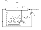
- FIG. 1 shows the feedback part of a standard second-order IIR filter 10 , which receives an input signal and outputs a filtered signal.
- the input is added to a first feedback signal in a first adding element 12 , added to a second feedback signal in a second adding element 14 , and then output from the filter as the filtered signal.
- the filtered signal is fed back through a first delay element 16 , and multiplied by a first coefficient a 1 in a multiplying element 18 to generate the second feedback signal.
- the delayed signal output from the first delay element 16 is further output to a second delay element 20 , and multiplied by a second coefficient a 2 in a second multiplier 22 to generate the first feedback signal.
- FIG. 2 shows a hardware implementation of a filter 50 which uses these coefficients.
- the filter 50 receives an input signal, which is added to various fed back signals as follows, and outputs a filtered signal.
- the filtered signal is fed back through a delay element 52 .
- the output from the delay element 52 is input to an adding element 54 , where it is added to the input signal.
- the output from the delay element 52 is also input to a further delay element 56 ; the output from the delay element 56 is inverted in an inverter 58 ; the output from the inverter 58 is multiplied by H 1 in a multiplying element 60 ; and the output from the multiplying element 60 is input to the adding element 54 .
- the output from the inverter 58 is further input to an adding element 62 , where it is added to the output from the delay element 52 ; the output from the adding element 62 is also to the adder 54 .
- the output from adding element 62 is further inverted in an inverter 64 ; the output from the inverter 64 is multiplied by H 0 in a multiplying element 66 ; and the output from the multiplying element 66 is also input to the adding element 54 .
- the filter 50 contains a functional group 70 of components, including the delay element 56 , the inverter 58 , the multiplying element 60 and the adding element 62 .
- the functional group 70 receives an input signal (in this case the delayed filtered signal output from the delay element 52 ) and outputs an inverted signal multiplied by an H coefficient, and a summed signal.
- out in+((1 ⁇ z ⁇ 1 )(1 ⁇ H 0 )+1 ⁇ H 1 z ⁇ 1 ) z ⁇ 1 out
- a second order Butterworth IIR low-pass filter was designed as an example.
- the coefficients required for the standard filter and for the invention are listed below for various ratios of sampling frequency to filter cut-off frequency.
- the conventional filter i.e. that which uses coefficients a 0 and a 1
- the coefficients need to be approximately 10 times more accurate.
- each increase by a factor of 10 in the frequency ratio simply scales the H 0 and H 1 coefficients of the invention down by a factor of approximately 10. If these coefficients are implemented with a combination of a bit-shift and a multiply, the multiplier itself is unchanged by this scaling. It is therefore a second object of the invention to provide a filter which is easily scalable in the frequency domain by such means.
- FIG. 3 shows the feedback part of a sixth-order IIR filter 100 according to the present invention.
- the filter 100 comprises five cascaded functional groups 70 A, 70 B, 70 C, 70 D and 70 E for multiplying by the coefficients H 5 , H 4 , H 3 , H 2 and H 1 , respectively.
- the filter 100 receives an input signal, which is added to various fed back signals as follows, and outputs a filtered signal.
- the filtered signal is fed back through a delay element 102 .
- the output from the delay element 102 is input to an adding element 104 , where it is added to the input signal.
- the output from the delay element 102 is also input to the first functional group 70 A.
- the multiplied output of the first functional group 70 A is output to a delay element 106 ; and the summed output of the first functional group 70 A is input to the adding element 104 , as well as the second function group 70 B.
- the multiplied output of the second functional group 70 B is output to an adding element 108 , where it is added to the output from the delay element 106 ; the summed output of the second functional group 70 B is input to the adding element 104 , as well as the third function group 70 C.
- the output from the adding element 108 is fed through a delay element 110 to an adding element 112 .
- the multiplied output of the third functional group 70 C is output to the adding element 112 , where it is added to the output from the delay element 110 ; the summed output of the third functional group 70 C is input to the adding element 104 , as well as the fourth function group 70 D.
- the output from the adding element 112 is fed through a delay element 114 to an adding element 116 .
- the multiplied output of the fourth functional group 70 D is output to the adding element 116 , where it is added to the output from the delay element 114 ; the summed output of the fourth functional group 70 D is input to the adding element 104 , as well as the fifth function group 70 E.
- the output from the adding element 116 is fed through a delay element 118 to an adding element 120 .
- the multiplied output of the fifth functional group 70 E is output to the adding element 120 , where it is added to the output from the delay element 118 ; the output from the adding element 120 is input to the adding element 104 . Further, the summed output of the fifth functional group 70 E is input to the adding element 104 , as well as an inverter 122 . The output from the inverter 122 is fed to a multiplier 124 , where it is multiplied by a coefficient H 0 , and the output from the multiplier 124 is input to the adding element 104 .
- the coefficients H 0 to H 5 can be represented by a bit shift and a coefficient with relatively few bits of precision. It can be proven that the architecture of FIG. 3 is mathematically equivalent to the original cascade of three second-order sections. The advantage of the invention is however clear: there are only six multiplies required, each of which requires a low-precision coefficient. For the same filter performance, the standard arrangement would require much higher multiplier precision.
- first-order terms are the A X coefficients, where the subscript X is A, B or C.
- Second-order terms are the B X coefficients and products of two different A X coefficients (i.e. A X .A Y , where the subscripts X and Y are different).
- Third-order terms are products of three A X coefficients, or one A X and one B X coefficient, and so on.
- H 0 is the sum of the first-order terms
- H 1 is the sum of the second-order terms
- H 2 is the sum of third-order terms
- H 5 is the sum of sixth-order terms, of which there is only one.
- a fourth-order Butterworth low-pass filter with a cut-off frequency of 200 Hz and a sample rate of 3.072 MHz was designed using a standard filter design tool.
- coefficients would require 10 bits in order to represent the 0.999 part, and depending on the accuracy requirements, possibly a further 16 bits to represent the coefficient in sufficient detail—a total of 26 bits.
- H 0 0.547291813070848 ⁇ 2 ⁇ 9
- H 1 0.599 ⁇ 2 ⁇ 20
- H 2 0.768054549 ⁇ 2 ⁇ 32
- H 3 0.99786479768 ⁇ 2 ⁇ 45
- Each coefficient requires a different bit-shift to implement the scaling power of 2. It has been found by simulation that the normalised H coefficients can be implemented with 8 or fewer bits without significant loss of filter accuracy. Because of the differing bit shift, the data word length for the multipliers is also reduced. H 3 , for example, only requires a data word length of 64-45, i.e. 19 bits. It therefore requires a 19 ⁇ 8 bit multiplier, a considerable saving on the conventional 64 ⁇ 26 multiply.
- each H coefficient is approximately 212 times smaller than the previous a X coefficient in this example; thus each successive bit-shift is 12 bits higher than the previous one.
- the over-sampling ratio the higher the sampling frequency relative to the filter poles, the larger the ratio between H coefficients.
- This allows a programmable or variable filter to be implemented with a limited or even fixed set of bit-shifts; thus expensive barrel-shifters are not required.
- Knowledge of these bit-shifts also allows reduced-length adders to be used in some parts of the architecture.
- An alternative to cascading second-order sections as described above is to arrange second-order sections in parallel, with their inputs connected to a common point and their outputs summed to form the filter output.
- An example of a 4th order filter 300 arranged in this format is shown in FIG. 5 .
- the filter 300 includes substantially similar first and second second-order units, for multiplying by coefficients H A1 and H A0 , and H B1 and H B0 , respectively.
- the first unit receives an input signal and outputs a first intermediate filtered signal.
- the second unit also receives the input signal and generates a second intermediate filtered signal.
- the first and second intermediate filtered signals are summed in an adding element 302 , to generate the overall filtered output signal.
- an additional gain term G may be required as shown to implement some filters, that is, the input signal may also be input to the adding element 302 via a multiplying element 304 , for multiplying the input signal by a gain term G.
- the first intermediate filtered signal is fed back through a delay element 306 .
- the output from the delay element 306 is input to an adding element 308 , where it is added to the input signal.
- the output from the delay element 306 is also input to a first functional group 70 A′.
- the H A1 -multiplied output of the first functional group 70 A′ is output to the adding element 308 ; the summed output of the first functional group 70 A′ is output to the adding element 308 and an inverter 310 .
- the output from the inverter 310 is input to a multiplying element 312 , which multiplies it by the coefficient H A0 .
- the multiplied output from the multiplying element 312 is further input to the adding element 308 .
- the second intermediate filtered signal is fed back through a delay element 314 .
- the output from the delay element 314 is input to an adding element 316 , where it is added to the input signal.
- the output from the delay element 314 is also input to a second functional group 70 B′.
- the H B1 -multiplied output of the second functional group 70 B′ is output to the adding element 316 ; the summed output of the second functional group 70 B′ is output to the adding element 316 and an inverter 318 .
- the output from the inverter 318 is input to a multiplying element 320 , which multiplies it by the coefficient H B0 .
- the multiplied output from the multiplying element 320 is further input to the adding element 316 .
- the outputs from the adding elements 306 , 318 are then input to the adding element 302 as the first and second intermediate filtered signals, respectively.
- FIG. 6 a shows a direct implementation of the feed-forward part
- FIG. 6 b shows it split into three cascaded second-order sections. All the multipliers of FIG. 6 a receive the data input, which has only a few bits, or a single bit. The multipliers therefore require relatively few hardware or software resources to implement. In contrast, in FIG. 6 b , only the first stage has this advantage: the other stages have a long word-length input from the previous stage, and therefore require much larger multiplications.
- the method of FIG. 6 a is therefore preferred for these applications.
- the multipliers can be implemented by a hardware ROM or RAM, or software look-up table, as for example shown in FIG. 7 .
- further savings can be made by sharing the chain of input delay elements between all the second-order sections.
- the multipliers can be replaced by selectors (multiplexers) that select either the coefficient or its negated version, as shown in FIG. 8 , or by switchable negation stages, as shown in FIG. 9 , thus avoiding the use of any multipliers.
- processor control code for example on a carrier medium such as a disk, CD- or DVD-ROM, programmed memory such as read only memory (firmware), or on a data carrier such as an optical or electrical signal carrier.
- a carrier medium such as a disk, CD- or DVD-ROM, programmed memory such as read only memory (firmware), or on a data carrier such as an optical or electrical signal carrier.
- embodiments of the invention will be implemented on a DSP (digital signal processor), ASIC (application specific integrated circuit) or FPGA (field programmable gate array).
- the code may comprise conventional program code or microcode or, for example code for setting up or controlling an ASIC or FPGA.
- the code may also comprise code for dynamically configuring re-configurable apparatus such as re-programmable logic gate arrays.
- the code may comprise code for a hardware description language such as Verilog TM or VHDL (very high speed integrated circuit hardware description language).
- Verilog TM or VHDL very high speed integrated circuit hardware description language
- the code may be distributed between a plurality of coupled components in communication with one another.
- the embodiments may also be implemented using code running on a field-(re-)programmable analogue array or similar device in order to configure analogue/digital hardware.
Landscapes
- Engineering & Computer Science (AREA)
- Physics & Mathematics (AREA)
- Computer Hardware Design (AREA)
- Mathematical Physics (AREA)
- Computing Systems (AREA)
- Theoretical Computer Science (AREA)
- Compression, Expansion, Code Conversion, And Decoders (AREA)
- Filters That Use Time-Delay Elements (AREA)
- Cable Transmission Systems, Equalization Of Radio And Reduction Of Echo (AREA)
Abstract
Description
H 0=2+a 1
H 1=1+a 1 +a 2
out=in+((1−z −1)(1−H 0)+1−H 1 z −1)z −1out
(1+(H 0−2)z −1+(1−H 0 +H 1)z −2)×out=in
(1+a 1 z −1 +a 2 z −2)×out=in
| Frequency ratio | Coefficient a1 | Coefficient a2 | Coefficient H0 | Coefficient H1 |
| 10 | −1.14298050253 | 0.412801598096 | 0.85701949747 | 0.269821095566 |
| 100 | −1.91119706742 | 0.914975834801 | 0.08880293257 | 0.003778767375 |
| 1000 | −1.99111429220 | 0.991153595868 | 0.00888570779 | 0.000039303667 |
| 10000 | −1.999111423470 | 0.999111818079 | 0.00088857652 | 0.0000003946088 |
| 100000 | −1.999911142341 | 0.999911146288 | 0.00008885765 | 0.0000000039476 |
| Second-order | ||
| section number | Coefficient a1 | Coefficient a2 |
| 1 | a1A | a2A |
| 2 | a1B | a2B |
| 3 | a1C | a2C |
H 0 =A A +A B +A C
H 1 =A A A B +A A A C +A B A C +B A +B B +B C
H 2 =A A A B A C +A A(B B +B C)+A B(B A +B C)+A C(B A +B B)
H 3 =B A B B +B A B B +B B B C +A A A B B C +A A A C B B +A B A C B A
H 4 =B A B B A C +B A B C A B +B B B C A A
H5=BABBBC
where
A A=2+a 1A
B A=1+a 1A +a 2A
A B=2+a 1B
B B=1+a 1B +a 2B
A C=2+a 1C
B C=1+a 1C +a 2C
H 0 =A A +A B
H 1 =A A A B +B A +B B
H 2 =A A B B +A B B A
H3=BABB
where the Ax and Bx values are as defined earlier.
a 1A=−1.999239168990805
a2A=0.9992393400955952
a 1B=−1.999691901686791
a2B=0.9996920674391542
H 0=0.547291813070848×2−9
H 1=0.599×2−20
H 2=0.768054549×2−32
H 3=0.99786479768×2−45
Claims (8)
Applications Claiming Priority (3)
| Application Number | Priority Date | Filing Date | Title |
|---|---|---|---|
| GB0725116.8 | 2007-12-21 | ||
| GB0725116A GB2455806B (en) | 2007-12-21 | 2007-12-21 | Filter |
| PCT/GB2008/051183 WO2009081188A1 (en) | 2007-12-21 | 2008-12-12 | Filter |
Publications (2)
| Publication Number | Publication Date |
|---|---|
| US20100306297A1 US20100306297A1 (en) | 2010-12-02 |
| US8645444B2 true US8645444B2 (en) | 2014-02-04 |
Family
ID=39048665
Family Applications (1)
| Application Number | Title | Priority Date | Filing Date |
|---|---|---|---|
| US12/745,726 Expired - Fee Related US8645444B2 (en) | 2007-12-21 | 2008-12-12 | IIR filter for reducing the complexity of multiplying elements |
Country Status (3)
| Country | Link |
|---|---|
| US (1) | US8645444B2 (en) |
| GB (1) | GB2455806B (en) |
| WO (1) | WO2009081188A1 (en) |
Cited By (3)
| Publication number | Priority date | Publication date | Assignee | Title |
|---|---|---|---|---|
| TWI649970B (en) * | 2014-12-16 | 2019-02-01 | Samsung Electronics Co., Ltd. | Apparatus and method for DRAM type reconfigurable logic |
| US11948546B2 (en) | 2022-07-06 | 2024-04-02 | Cirrus Logic, Inc. | Feed-forward adaptive noise-canceling with dynamic filter selection based on classifying acoustic environment |
| US12340786B2 (en) | 2022-07-27 | 2025-06-24 | Cirrus Logic, Inc. | Adaptive noise-canceling with dynamic filter selection based on multiple noise sensor signal phase differences |
Families Citing this family (1)
| Publication number | Priority date | Publication date | Assignee | Title |
|---|---|---|---|---|
| US11652471B2 (en) * | 2020-06-30 | 2023-05-16 | Google Llc | Low power biquad systems and methods |
Citations (6)
| Publication number | Priority date | Publication date | Assignee | Title |
|---|---|---|---|---|
| US4255794A (en) | 1978-05-10 | 1981-03-10 | Nippon Electric Co., Ltd. | Digital filter |
| US5170369A (en) | 1989-09-25 | 1992-12-08 | E-Mu Systems, Inc. | Dynamic digital IIR audio filter and method which provides dynamic digital filtering for audio signals |
| US5487023A (en) * | 1994-02-14 | 1996-01-23 | Tektronix, Inc. | Repeatable finite and infinite impulse response integrated circuit structure |
| US5629881A (en) | 1994-03-15 | 1997-05-13 | Siemens Aktiengesellschaft | Method for filtering a digital value train with improved noise behavior, and circuit configuration for performing the method |
| US5717726A (en) | 1993-03-24 | 1998-02-10 | Robert Bosch Gmbh | Digital filter |
| EP0948133A2 (en) | 1998-03-30 | 1999-10-06 | Texas Instruments Incorporated | Digital filter with efficient quantization circuitry |
-
2007
- 2007-12-21 GB GB0725116A patent/GB2455806B/en active Active
-
2008
- 2008-12-12 WO PCT/GB2008/051183 patent/WO2009081188A1/en not_active Ceased
- 2008-12-12 US US12/745,726 patent/US8645444B2/en not_active Expired - Fee Related
Patent Citations (6)
| Publication number | Priority date | Publication date | Assignee | Title |
|---|---|---|---|---|
| US4255794A (en) | 1978-05-10 | 1981-03-10 | Nippon Electric Co., Ltd. | Digital filter |
| US5170369A (en) | 1989-09-25 | 1992-12-08 | E-Mu Systems, Inc. | Dynamic digital IIR audio filter and method which provides dynamic digital filtering for audio signals |
| US5717726A (en) | 1993-03-24 | 1998-02-10 | Robert Bosch Gmbh | Digital filter |
| US5487023A (en) * | 1994-02-14 | 1996-01-23 | Tektronix, Inc. | Repeatable finite and infinite impulse response integrated circuit structure |
| US5629881A (en) | 1994-03-15 | 1997-05-13 | Siemens Aktiengesellschaft | Method for filtering a digital value train with improved noise behavior, and circuit configuration for performing the method |
| EP0948133A2 (en) | 1998-03-30 | 1999-10-06 | Texas Instruments Incorporated | Digital filter with efficient quantization circuitry |
Cited By (3)
| Publication number | Priority date | Publication date | Assignee | Title |
|---|---|---|---|---|
| TWI649970B (en) * | 2014-12-16 | 2019-02-01 | Samsung Electronics Co., Ltd. | Apparatus and method for DRAM type reconfigurable logic |
| US11948546B2 (en) | 2022-07-06 | 2024-04-02 | Cirrus Logic, Inc. | Feed-forward adaptive noise-canceling with dynamic filter selection based on classifying acoustic environment |
| US12340786B2 (en) | 2022-07-27 | 2025-06-24 | Cirrus Logic, Inc. | Adaptive noise-canceling with dynamic filter selection based on multiple noise sensor signal phase differences |
Also Published As
| Publication number | Publication date |
|---|---|
| GB0725116D0 (en) | 2008-01-30 |
| GB2455806A (en) | 2009-06-24 |
| US20100306297A1 (en) | 2010-12-02 |
| GB2455806B (en) | 2010-04-14 |
| WO2009081188A1 (en) | 2009-07-02 |
Similar Documents
| Publication | Publication Date | Title |
|---|---|---|
| Sumalatha et al. | Low power and low area VLSI implementation of vedic design FIR filter for ECG signal de-noising | |
| US6263354B1 (en) | Reduced multiplier digital IIR filters | |
| EP3153963B1 (en) | Methods and apparatus for sequencing arithmetic operations | |
| US8645444B2 (en) | IIR filter for reducing the complexity of multiplying elements | |
| Guo et al. | A novel adaptive filter implementation scheme using distributed arithmetic | |
| US5383145A (en) | Digital filter and digital signal processing system | |
| Keerthi et al. | FPGA implementation of distributed arithmetic for FIR filter | |
| US20100077014A1 (en) | Second order real allpass filter | |
| Datta et al. | FPGA implementation of symmetric systolic FIR filter using multi-channel technique | |
| Kumar et al. | Low area VLSI implementation of CSLA for FIR filter design | |
| US20080225937A1 (en) | Method and system of providing a high speed tomlinson-harashima precoder | |
| US5928314A (en) | Digital filter having a substantially equal number of negative and positive weighting factors | |
| Paliwal et al. | Efficient FPGA implementation architecture of fast FIR algorithm using Han-Carlson adder based vedic multiplier | |
| WO2005002051A1 (en) | Digital filter | |
| Yadav et al. | Comparative analysis of digital IIR filter using add and shift method on Xilinx platform | |
| Raj et al. | A paradigm of distributed arithmetic (DA) approaches for digital FIR filter | |
| Narasimha et al. | Implementation of low area and power efficient architectures for digital FIR filters | |
| Meher | Low-latency hardware-efficient memory-based design for large-order FIR digital filters | |
| Jayashree | Design of high speed and area efficient FIR filter architecture using modified adder and multiplier | |
| KR102667990B1 (en) | Filter and Method with Multiplication Operation Approximation Capability | |
| Ali | Cascaded ripple carry adder based SRCSA for efficient FIR filter | |
| US11652471B2 (en) | Low power biquad systems and methods | |
| JPH0575394A (en) | Digital filter and digital signal processing system | |
| Langlois | Design and Implementation of High Sampling Rate Programmable FIR Filters in FPGAs | |
| Gupta et al. | LUT and LUT-Less Multiplier Architecture for Low Power Adaptive Filter |
Legal Events
| Date | Code | Title | Description |
|---|---|---|---|
| AS | Assignment |
Owner name: WOLFSON MICROELECTRONICS PLC, UNITED KINGDOM Free format text: ASSIGNMENT OF ASSIGNORS INTEREST;ASSIGNORS:CLEMOW, RICHARD DAVID;MAGRATH, ANTHONY JAMES;SIGNING DATES FROM 20100708 TO 20100816;REEL/FRAME:024852/0510 |
|
| STCF | Information on status: patent grant |
Free format text: PATENTED CASE |
|
| AS | Assignment |
Owner name: WOLFSON MICROELECTRONICS LTD, UNITED KINGDOM Free format text: CHANGE OF NAME;ASSIGNOR:WOLFSON MICROELECTRONICS PLC;REEL/FRAME:035356/0096 Effective date: 20140821 Owner name: CIRRUS LOGIC INTERNATIONAL (UK) LTD., UNITED KINGD Free format text: CHANGE OF NAME;ASSIGNOR:WOLFSON MICROELECTRONICS LTD;REEL/FRAME:035353/0413 Effective date: 20141127 |
|
| AS | Assignment |
Owner name: CIRRUS LOGIC INTERNATIONAL SEMICONDUCTOR LTD., UNI Free format text: ASSIGNMENT OF ASSIGNORS INTEREST;ASSIGNOR:CIRRUS LOGIC INTERNATIONAL (UK) LTD.;REEL/FRAME:035806/0389 Effective date: 20150329 |
|
| AS | Assignment |
Owner name: CIRRUS LOGIC INC., TEXAS Free format text: ASSIGNMENT OF ASSIGNORS INTEREST;ASSIGNOR:CIRRUS LOGIC INTERNATIONAL SEMICONDUCTOR LTD.;REEL/FRAME:035909/0190 Effective date: 20150329 |
|
| CC | Certificate of correction | ||
| FPAY | Fee payment |
Year of fee payment: 4 |
|
| FEPP | Fee payment procedure |
Free format text: MAINTENANCE FEE REMINDER MAILED (ORIGINAL EVENT CODE: REM.); ENTITY STATUS OF PATENT OWNER: LARGE ENTITY |
|
| LAPS | Lapse for failure to pay maintenance fees |
Free format text: PATENT EXPIRED FOR FAILURE TO PAY MAINTENANCE FEES (ORIGINAL EVENT CODE: EXP.); ENTITY STATUS OF PATENT OWNER: LARGE ENTITY |
|
| STCH | Information on status: patent discontinuation |
Free format text: PATENT EXPIRED DUE TO NONPAYMENT OF MAINTENANCE FEES UNDER 37 CFR 1.362 |
|
| FP | Lapsed due to failure to pay maintenance fee |
Effective date: 20220204 |