US8640332B2 - Method of manufacturing a stacked foil sheet device - Google Patents
Method of manufacturing a stacked foil sheet device Download PDFInfo
- Publication number
- US8640332B2 US8640332B2 US12/823,946 US82394610A US8640332B2 US 8640332 B2 US8640332 B2 US 8640332B2 US 82394610 A US82394610 A US 82394610A US 8640332 B2 US8640332 B2 US 8640332B2
- Authority
- US
- United States
- Prior art keywords
- foil sheet
- foil
- reel
- length direction
- stacked
- Prior art date
- Legal status (The legal status is an assumption and is not a legal conclusion. Google has not performed a legal analysis and makes no representation as to the accuracy of the status listed.)
- Expired - Fee Related, expires
Links
Images


Classifications
-
- H—ELECTRICITY
- H05—ELECTRIC TECHNIQUES NOT OTHERWISE PROVIDED FOR
- H05K—PRINTED CIRCUITS; CASINGS OR CONSTRUCTIONAL DETAILS OF ELECTRIC APPARATUS; MANUFACTURE OF ASSEMBLAGES OF ELECTRICAL COMPONENTS
- H05K3/00—Apparatus or processes for manufacturing printed circuits
- H05K3/46—Manufacturing multilayer circuits
- H05K3/4611—Manufacturing multilayer circuits by laminating two or more circuit boards
- H05K3/4638—Aligning and fixing the circuit boards before lamination; Detecting or measuring the misalignment after lamination; Aligning external circuit patterns or via connections relative to internal circuits
-
- H—ELECTRICITY
- H05—ELECTRIC TECHNIQUES NOT OTHERWISE PROVIDED FOR
- H05K—PRINTED CIRCUITS; CASINGS OR CONSTRUCTIONAL DETAILS OF ELECTRIC APPARATUS; MANUFACTURE OF ASSEMBLAGES OF ELECTRICAL COMPONENTS
- H05K3/00—Apparatus or processes for manufacturing printed circuits
- H05K3/46—Manufacturing multilayer circuits
- H05K3/4611—Manufacturing multilayer circuits by laminating two or more circuit boards
- H05K3/4626—Manufacturing multilayer circuits by laminating two or more circuit boards characterised by the insulating layers or materials
- H05K3/4635—Manufacturing multilayer circuits by laminating two or more circuit boards characterised by the insulating layers or materials laminating flexible circuit boards using additional insulating adhesive materials between the boards
-
- H—ELECTRICITY
- H05—ELECTRIC TECHNIQUES NOT OTHERWISE PROVIDED FOR
- H05K—PRINTED CIRCUITS; CASINGS OR CONSTRUCTIONAL DETAILS OF ELECTRIC APPARATUS; MANUFACTURE OF ASSEMBLAGES OF ELECTRICAL COMPONENTS
- H05K1/00—Printed circuits
- H05K1/02—Details
- H05K1/03—Use of materials for the substrate
- H05K1/0393—Flexible materials
-
- H—ELECTRICITY
- H05—ELECTRIC TECHNIQUES NOT OTHERWISE PROVIDED FOR
- H05K—PRINTED CIRCUITS; CASINGS OR CONSTRUCTIONAL DETAILS OF ELECTRIC APPARATUS; MANUFACTURE OF ASSEMBLAGES OF ELECTRICAL COMPONENTS
- H05K2201/00—Indexing scheme relating to printed circuits covered by H05K1/00
- H05K2201/05—Flexible printed circuits [FPCs]
- H05K2201/051—Rolled
-
- H—ELECTRICITY
- H05—ELECTRIC TECHNIQUES NOT OTHERWISE PROVIDED FOR
- H05K—PRINTED CIRCUITS; CASINGS OR CONSTRUCTIONAL DETAILS OF ELECTRIC APPARATUS; MANUFACTURE OF ASSEMBLAGES OF ELECTRICAL COMPONENTS
- H05K2201/00—Indexing scheme relating to printed circuits covered by H05K1/00
- H05K2201/09—Shape and layout
- H05K2201/09009—Substrate related
- H05K2201/09036—Recesses or grooves in insulating substrate
-
- H—ELECTRICITY
- H05—ELECTRIC TECHNIQUES NOT OTHERWISE PROVIDED FOR
- H05K—PRINTED CIRCUITS; CASINGS OR CONSTRUCTIONAL DETAILS OF ELECTRIC APPARATUS; MANUFACTURE OF ASSEMBLAGES OF ELECTRICAL COMPONENTS
- H05K2201/00—Indexing scheme relating to printed circuits covered by H05K1/00
- H05K2201/09—Shape and layout
- H05K2201/09009—Substrate related
- H05K2201/09045—Locally raised area or protrusion of insulating substrate
-
- H—ELECTRICITY
- H05—ELECTRIC TECHNIQUES NOT OTHERWISE PROVIDED FOR
- H05K—PRINTED CIRCUITS; CASINGS OR CONSTRUCTIONAL DETAILS OF ELECTRIC APPARATUS; MANUFACTURE OF ASSEMBLAGES OF ELECTRICAL COMPONENTS
- H05K2201/00—Indexing scheme relating to printed circuits covered by H05K1/00
- H05K2201/09—Shape and layout
- H05K2201/09009—Substrate related
- H05K2201/09063—Holes or slots in insulating substrate not used for electrical connections
-
- H—ELECTRICITY
- H05—ELECTRIC TECHNIQUES NOT OTHERWISE PROVIDED FOR
- H05K—PRINTED CIRCUITS; CASINGS OR CONSTRUCTIONAL DETAILS OF ELECTRIC APPARATUS; MANUFACTURE OF ASSEMBLAGES OF ELECTRICAL COMPONENTS
- H05K2201/00—Indexing scheme relating to printed circuits covered by H05K1/00
- H05K2201/09—Shape and layout
- H05K2201/09009—Substrate related
- H05K2201/091—Locally and permanently deformed areas including dielectric material
-
- H—ELECTRICITY
- H05—ELECTRIC TECHNIQUES NOT OTHERWISE PROVIDED FOR
- H05K—PRINTED CIRCUITS; CASINGS OR CONSTRUCTIONAL DETAILS OF ELECTRIC APPARATUS; MANUFACTURE OF ASSEMBLAGES OF ELECTRICAL COMPONENTS
- H05K2203/00—Indexing scheme relating to apparatus or processes for manufacturing printed circuits covered by H05K3/00
- H05K2203/01—Tools for processing; Objects used during processing
- H05K2203/0104—Tools for processing; Objects used during processing for patterning or coating
- H05K2203/0108—Male die used for patterning, punching or transferring
-
- H—ELECTRICITY
- H05—ELECTRIC TECHNIQUES NOT OTHERWISE PROVIDED FOR
- H05K—PRINTED CIRCUITS; CASINGS OR CONSTRUCTIONAL DETAILS OF ELECTRIC APPARATUS; MANUFACTURE OF ASSEMBLAGES OF ELECTRICAL COMPONENTS
- H05K2203/00—Indexing scheme relating to apparatus or processes for manufacturing printed circuits covered by H05K3/00
- H05K2203/02—Details related to mechanical or acoustic processing, e.g. drilling, punching, cutting, using ultrasound
- H05K2203/0228—Cutting, sawing, milling or shearing
-
- H—ELECTRICITY
- H05—ELECTRIC TECHNIQUES NOT OTHERWISE PROVIDED FOR
- H05K—PRINTED CIRCUITS; CASINGS OR CONSTRUCTIONAL DETAILS OF ELECTRIC APPARATUS; MANUFACTURE OF ASSEMBLAGES OF ELECTRICAL COMPONENTS
- H05K2203/00—Indexing scheme relating to apparatus or processes for manufacturing printed circuits covered by H05K3/00
- H05K2203/16—Inspection; Monitoring; Aligning
- H05K2203/167—Using mechanical means for positioning, alignment or registration, e.g. using rod-in-hole alignment
-
- H—ELECTRICITY
- H05—ELECTRIC TECHNIQUES NOT OTHERWISE PROVIDED FOR
- H05K—PRINTED CIRCUITS; CASINGS OR CONSTRUCTIONAL DETAILS OF ELECTRIC APPARATUS; MANUFACTURE OF ASSEMBLAGES OF ELECTRICAL COMPONENTS
- H05K3/00—Apparatus or processes for manufacturing printed circuits
- H05K3/40—Forming printed elements for providing electric connections to or between printed circuits
- H05K3/4038—Through-connections; Vertical interconnect access [VIA] connections
- H05K3/4053—Through-connections; Vertical interconnect access [VIA] connections by thick-film techniques
- H05K3/4069—Through-connections; Vertical interconnect access [VIA] connections by thick-film techniques for via connections in organic insulating substrates
-
- Y—GENERAL TAGGING OF NEW TECHNOLOGICAL DEVELOPMENTS; GENERAL TAGGING OF CROSS-SECTIONAL TECHNOLOGIES SPANNING OVER SEVERAL SECTIONS OF THE IPC; TECHNICAL SUBJECTS COVERED BY FORMER USPC CROSS-REFERENCE ART COLLECTIONS [XRACs] AND DIGESTS
- Y10—TECHNICAL SUBJECTS COVERED BY FORMER USPC
- Y10T—TECHNICAL SUBJECTS COVERED BY FORMER US CLASSIFICATION
- Y10T156/00—Adhesive bonding and miscellaneous chemical manufacture
- Y10T156/10—Methods of surface bonding and/or assembly therefor
- Y10T156/1002—Methods of surface bonding and/or assembly therefor with permanent bending or reshaping or surface deformation of self sustaining lamina
- Y10T156/1039—Surface deformation only of sandwich or lamina [e.g., embossed panels]
-
- Y—GENERAL TAGGING OF NEW TECHNOLOGICAL DEVELOPMENTS; GENERAL TAGGING OF CROSS-SECTIONAL TECHNOLOGIES SPANNING OVER SEVERAL SECTIONS OF THE IPC; TECHNICAL SUBJECTS COVERED BY FORMER USPC CROSS-REFERENCE ART COLLECTIONS [XRACs] AND DIGESTS
- Y10—TECHNICAL SUBJECTS COVERED BY FORMER USPC
- Y10T—TECHNICAL SUBJECTS COVERED BY FORMER US CLASSIFICATION
- Y10T29/00—Metal working
- Y10T29/49—Method of mechanical manufacture
- Y10T29/49002—Electrical device making
- Y10T29/49117—Conductor or circuit manufacturing
- Y10T29/49124—On flat or curved insulated base, e.g., printed circuit, etc.
- Y10T29/49155—Manufacturing circuit on or in base
Definitions
- the invention relates to a method of manufacturing a stacked device wherein a plurality of flexible foil sheets is provided each having device functionality zones.
- a main advantage of (plastic) electronics on flexible foil sheets is the large-scale, cost-efficient production and manufacturing potential. These devices are currently manufactured in batch-wise production. However, this manufacturing process is time consuming, and alignment of each of the layers needs to be done separately.
- the invention aims to provide a method of manufacturing a stacked device wherein the production speed of the manufacturing process is substantially improved.
- WO2006061361 discloses an optical data memory on cylindrical core, wherein stacked layers are provided each having an optical data memory function.
- a method is provided of manufacturing a stacked device, comprising: providing a foil sheet having device functionality zones; aligning the device functionality zones in the foil sheet to form stacked foil sheets on a reel having a reel radius, electrically connecting at least some of the device functionality zones; and separating the stacked foil sheets from the reel to form the stacked foil sheet device.
- a 3D flexible foil sheet electronics medium can be made by stacking multiple foils on top of each other and high throughput roll-to-roll or roll-to-sheet production methods, like utilized in the newspaper printing business are made possible.
- FIG. 1 shows a schematic embodiment according to the invention
- FIG. 2 shows a schematic illustration of a winding arrangement according to an aspect of the invention
- FIG. 3 shows a detailed view of the winding arrangement of FIG. 2 ;
- FIG. 4 shows a plurality of alignment markers according to another aspect of the invention.
- FIG. 5 shows one manufacturing embodiment to provide the alignment markers depicted in FIG. 4 ;
- FIG. 6 shows another manufacturing embodiment to provide the alignment markers of FIG. 4 ;
- FIG. 7 shows a plurality of weakenings according to yet another aspect of the invention.
- FIG. 1 schematically shows a proposed manufacturing process of a stacked device 100 .
- a three-dimensional wound medium is provided wherein device functionality zones 3 , also called information zones are aligned.
- device functionality zones 3 also called information zones are aligned.
- a lamination layer 21 is provided for laminating the stacked layers to each other, for example, by providing a glue.
- the device 100 can be cut off from the reel 4 along cut 25 . Where in the application the term reel is used, this conforms to any 3D medium that can be used to wind the foil sheet 2 .
- a method in which a smart way of foil stacking is provided.
- the method allows for stacking multiple layers to a three-dimensional device 100 and facilitates the via-drilling tremendously.
- Vias 23 can be formed during, or after complete winding by mechanical drilling, laser drilling or laser conversion of the stacked foil sheet layers 20 on the reel 4 .
- the proposed type of alignment can facilitate the interconnect drilling and interconnects along a radial direction of the reel 4 can be made by single via drilling through the multiple layers.
- a foil sheet 2 may comprise one or more supporting flexible carriers with a functional stack of layers provided thereon and possibly a protection layer.
- the functional stack typically comprises several different films or layers. It is explicitly mentioned that the definition of layer or foil sheet is not limited to the described embodiments.
- the anticipated types of devices in particular, electronic circuitry on large flexible foil sheets 20
- can be used in a variety of applications such as flexible displays, rollable displays, large sensor arrays, flexible lighting tiles and signage devices, solar cells on foils, batteries on foils, etc.
- One advantage of these products is the flexibility of the considered foil sheets 20 , in particular, if foil sheets 20 are based on organic flexible foil carriers, such as PEN or PET materials.
- the foil sheets 20 can be reversibly deformed, such that they are used in, for example, a rollable display application or in products with specific shapes, for example, a curved display on a dashboard.
- a further advantage of these devices is the limited thickness of the anticipated flexible foil sheets 20 , such that several foil sheets 20 can be stacked in a 3-dimensional device 100 .
- Hundreds of foil sheets 20 can be easily stacked.
- Examples of multi-foil approaches are the energy foil (battery foils are attached to a photovoltaic foil), a sensor foil (foil with photo-detectors, diodes and power foils), and a storage foil (with hundreds of attached foils), etc.
- interconnects or micro-vias 23 between the circuitry can be provided, for instance by laser drilling and subsequent via filling is common practice for making such micro-vias 23 but require careful alignment. Careful alignment is also required in the proposed device 100 , but the self-alignment function of the alignment markers 6 facilitates the via-drilling process.
- the foil sheet 2 comprises device functionality zones 3 , also called information zones.
- electronic circuitry is provided, for example, via layer deposition and patterning (lithography, direct laser writing, etc.). The deposition and patterning of the circuitry can be done before or after the creation of the alignment markers 6 .
- the foil sheet 2 may also comprise deformation zones 80 , in which deformation areas are present, and alignment marker zones, in which the alignment markers 6 (see FIG. 3 ) are present.
- layout contacts, or interconnects can be provided, to provide electronic contact between subsequent stacked layers. Accordingly, for a layer N in a stack of layers, layers N ⁇ 1 and N+1 can be addressed.
- a method of manufacturing a stacked device 100 comprising: providing a foil sheet 2 having device functionality zones 3 ; aligning the device functionality zones 3 in the flexible foil sheets 20 to form stacked foil sheets 20 on a reel 4 having a reel radius, electrically interconnecting at least some of the stacked device functionality zones 3 ; and separating the stacked foil sheets 20 from the reel 4 to form the stacked foil sheet layered device 100 .
- the method can be applied to produce a single device 100 to be cut from a reel 4 , also multiple stacks of stacked devices can be cut from a single reel 4 . For example, along a reel radius direction, a plurality of devices can be provided. Also, several stacks of devices may be produced, for instance by separating the interfacing layers of adjacent devices from each other along a radius of the wound reel 4 .
- the three-dimensional medium can be diced in pieces after via drilling and processing to reveal functional 3D devices.
- the deformation and alignment zones can be purposely left out of the 3D devices. Possible applications: batteries, memories, sensor arrays, etc.
- the three-dimensional electrode scheme enables, for instance, parallel processing.
- FIG. 2 shows a typical example of a wound 3-dimensional medium. It shows that the functionality zones 3 (see FIG. 1 ) are distanced as a function of reel radius and foil-sheet thickness. Accordingly, electronic interaction between the foil sheets 20 (layers) can be provided in a reel production process. Alignment of the stacked foil sheet layers is enhanced by providing alignment markers 6 (see FIG. 3 ), to be used to align the different windings 5 with respect to each other.
- the circumferential mismatch is constant for each winding: 2 ⁇ t, with t the thickness of the foil sheet 2 .
- the total circumferential mismatch is 2 ⁇ (N ⁇ 1)t.
- FIG. 3 shows an illustrative location of alignment markers 6 for 3D alignment of wound layers.
- a single alignment marker is provided per winding 5 , this can be varied in principally, for example, multiple alignment markers 6 can be provided per winding 5 (see FIG. 2 ), or an alignment marker can be provided per predefined number of windings 5 .
- the alignment markers 6 will influence the device functionality zone 3 , and therefore, in principle, the markers 6 are preferably separated from the device functionality zone 3 .
- mismatch due to foil sheet thickness also may occur to the information zone. For example, if the thickness of the foil is 25 micron, the mismatch is 50 ⁇ micron.
- FIG. 4 shows a preferred embodiment of the alignment markers 6 .
- these markers may be visual marks or otherwise detectable marks, preferably, the markers 6 are preferably arranged in marker zones, wherein embossed markers 6 are provided on the top and bottom of the foil sheet 2 .
- the markers 6 on one face side are ‘cutaways’ or recesses 62 ; the markers 6 of the other face side are protrusions 61 .
- a typical shape of an embossed marker 6 is given in FIG. 4A .
- FIG. 4B gives top views of possible other embodiments of the two-dimensional alignment marker.
- the shape of the marker 6 can also represent a unique code (kind of watermarking of encoding feature).
- the method comprises providing multiple alignment markers 6 in the foil sheet 2 , distanced conform the reel radius and each having an mark length direction transverse to the first foil sheet length direction, to form protrusions 61 and corresponding recesses; winding the foil sheet 2 on the reel 4 (see FIGS. 1 and 2 ) in the first foil sheet length direction of the foil sheet 2 ; and co-aligning the alignment markers 6 to have protrusions 61 of one mark matching with a recess of another mark, so as to align the stacked foil sheet layers 20 (see FIG. 2 ) in the first foil sheet length direction.
- alignment markers 6 may have protrusions 61 and recesses formed on opposing faces of a foil sheet 2 , this can be varied in principle, by having other connection schemes, for instance, by folding a single sheet 2 prior to winding the sheet 2 to a reel 4 . Also, by having multiple sheets wound on a reel 4 in a stacked configuration, protrusions 61 of one sheet 2 may correspond to recesses of another sheet 2 in the stack; prior to winding. In such schemes, a single foil sheet 2 may comprise protrusions 61 or recesses or a combination thereof on each opposite face of the sheet 2 .
- protrusions 61 provided on one face of the stack, and recesses on the other face of the stack, to conform to each other when wound on the reel 4 .
- said one and said another matching alignment markers 6 are adjacent to form a single marker zone 7 along the reel circumference.
- the alignment markers 6 are distanced as a function of reel radius and foil sheet thickness.
- the protrusions 61 and corresponding recesses are preferably provided with faces 63 aligned with the foil sheet normal direction.
- the alignment markers 6 may be formed to provide relative movement along the alignment marker length direction, preferably, to block such movement, they are provided with an interlocking form to block relative movement of the stacked foil sheets 20 in a direction transverse to the first foil sheet length direction.
- An example of such a form is given in FIG. 4 .
- the alignment markers 6 may be formed to have a second alignment marker length direction aligned with the first foil sheet length direction, so as to block relative movement of the stacked foil sheet layers transverse to the first length direction.
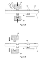
- FIG. 5 and FIG. 6 show examples of replication of the embossed alignment markers 6 (see FIG. 3 ) in the foil.
- the alignment markers 6 may provided by hot embossing through drums 90 , 91 foil sheet 2 or, according to the embodiment of FIG. 6 , by shaping a curable layer provided on the foil sheet 2 .
- a thin curable layer 24 is applied on top of the foil 2 via, for instance, slot die coating or gravure printing.
- the top markers (in this example, recesses) are present in the drums 90 as protrusions 61 and replicated in the foil sheet 2 as recesses 62 during the rolling process.
- the deposited layer 24 may be instantaneously cured via UV or heat.
- the markers 6 can be made via laser milling or by some other prefabrication method so that markers are already present in the foil sheet 2 before processing the foil sheet 2 .
- the bottom markers in this example, protrusions 61
- the top and bottom drums are synchronized such that the relative position between the top and bottom markers is fixed.
- the markers 6 may be made via punching (plastic deformation).
- FIG. 7 shows typical examples of deformation zones 8 , 800 , 801 to compensate for misalignment.
- the deformation zones typically comprise weakenings, such as perforated areas 8 , or areas having reduced thickness 801 or otherwise treated area 800 to provide a weakened zone.
- deformation zones typically contain perforations or holes made via laser drilling, laser milling, hot embossing, mechanical punching, or the deformation zones may have a reduced thickness.
- the deformation zones 8 may have a reduced tensile strength (lower Young's modulus via UV exposure, CO2 plasma treatment, etc.).
- the deformation areas 8 can thus be used to compensate for the possible mismatches in the length between subsequent alignment markers 6 (see FIG. 3 ).
- a three-dimensional perfectly aligned 3-dimensional device 100 results.
- the weakenings 8 can be dispensed with if the information zone 3 is distanced to compensate for foil sheet thickness, typically, while keeping the distance constant for each winding 5 (see FIG. 2 ), preferably, a plurality of weakenings 8 is provided in the foil sheet 2 for alignment purposes, to conform with a foil sheet thickness.
- the weakening 8 can typically be applied per each winding 5 , also multiple weakenings can be provided per winding 5 , or a weakening can be provided for a number of windings 5 .
- the weakenings are distanced to correspond to a single weakening zone along the reel circumference. Also, preferably the weakening zone is coinciding with an mark zone.
- the foil is provided with deformation zones 8 to compensate for possible mismatches in the distances between the two-dimensional alignment markers 6 .
- the embodiments show a single foil sheet 2 (see FIGS. 1 , 2 and 3 ) that is wound around a reel 4 (see FIGS. 1 and 2 ), in practice, as indicated, the foil sheet 2 may be a of composite nature, possibly comprising multiple carriers each with stacked additional layers, which may or may not be interconnected in advance. Typically, additional layers may be provided by glue or another connection process such as laser moulding etc.
- multiple foil sheets 20 may be fed into a winding process, wherein alignment between the multiple foil sheets 20 is provided by the hereabove described alignment markers 6 . In this way a stacked series of multiple foil sheets can be laminated.
- a battery foil and photovoltaic foil may be produced separately, provided by alignment markers 6 and deformation areas and stacked together via the proposed method. In that case, the alignment markers 6 on top and bottom may have the same polarity as well.
- a flexible foil sheet 2 can be aligned on a reel 4 having a reel radius, the foil sheet 2 having a general first foil sheet length direction, by providing multiple alignment markers 6 (see FIG. 3 ) in the foil sheet 2 (see FIGS. 1 , 2 and 3 ), distanced conform the reel radius and each having an alignment marker length direction transverse to the first foil sheet length direction, to form protrusions 61 (see FIGS. 4 and 5 ) and corresponding recesses on opposite faces of the foil sheet 2 ; winding the foil sheet 2 on the reel 4 (see FIGS.
- foil sheets 20 may be folded in advance according to a predetermined manner, for instance, to provide folded information zones. By folding foil sheets 20 , alignment markers 6 may be placed in an alternating manner, and the circumferential mismatch due folding in the bending areas may be carefully considered.
Landscapes
- Engineering & Computer Science (AREA)
- Manufacturing & Machinery (AREA)
- Microelectronics & Electronic Packaging (AREA)
- Storage Of Web-Like Or Filamentary Materials (AREA)
Abstract
Description
-
- Divide information zone is M parts, synchronize parts such that the mismatch is only 2 pd/M is about 1 micron in case of 25 micron thick films and 100 parts (M=100).
- The contact pads for contacting the vias 23 (see
FIG. 1 ) are designed such that they can compensate the mismatch. - The
alignment markers 6 and thedeformation markers 8 are located in the so-called alignment marker zone 7 and deformation marker zone 80 (seeFIGS. 1 and 2 ). By deforming thedeformation zone 8, aninformation zone 4 may remain having the same circumferential length such that the alignment of each winding (layer) is ensured. Here, it is contemplated, that preferably, thealignment markers 6 are provided in a single marker zone 7. Accordingly, preferably, the nth functionality zone 3 distance dn counted from a first winding 5, satisfies 1*dn=2*p*m*(R+n*t) forarbitrary integers 1 and m; and for a foil sheet thickness t and reel radius R.
Claims (19)
Applications Claiming Priority (5)
| Application Number | Priority Date | Filing Date | Title |
|---|---|---|---|
| EP07150452 | 2007-12-27 | ||
| EP07150452.6 | 2007-12-27 | ||
| EP07150452A EP2076099A1 (en) | 2007-12-27 | 2007-12-27 | Stacked foil sheet device |
| PCT/NL2008/050855 WO2009084958A1 (en) | 2007-12-27 | 2008-12-29 | Stacked foil sheet device |
| NLPCT/NL2008/050855 | 2008-12-29 |
Related Parent Applications (1)
| Application Number | Title | Priority Date | Filing Date |
|---|---|---|---|
| PCT/NL2008/050855 Continuation WO2009084958A1 (en) | 2007-12-27 | 2008-12-29 | Stacked foil sheet device |
Publications (3)
| Publication Number | Publication Date |
|---|---|
| US20110048619A1 US20110048619A1 (en) | 2011-03-03 |
| US20130306227A9 US20130306227A9 (en) | 2013-11-21 |
| US8640332B2 true US8640332B2 (en) | 2014-02-04 |
Family
ID=39365734
Family Applications (1)
| Application Number | Title | Priority Date | Filing Date |
|---|---|---|---|
| US12/823,946 Expired - Fee Related US8640332B2 (en) | 2007-12-27 | 2010-06-25 | Method of manufacturing a stacked foil sheet device |
Country Status (3)
| Country | Link |
|---|---|
| US (1) | US8640332B2 (en) |
| EP (2) | EP2076099A1 (en) |
| WO (1) | WO2009084958A1 (en) |
Families Citing this family (18)
| Publication number | Priority date | Publication date | Assignee | Title |
|---|---|---|---|---|
| EP2076099A1 (en) | 2007-12-27 | 2009-07-01 | Nederlandse Organisatie voor toegepast- natuurwetenschappelijk onderzoek TNO | Stacked foil sheet device |
| US20120118369A1 (en) * | 2010-10-15 | 2012-05-17 | Justin Hedtke | Solar cell architecture having a plurality of vias with shaped foil via interior |
| WO2012128909A2 (en) * | 2011-03-18 | 2012-09-27 | Applied Materials, Inc. | Process for forming flexible substrates using punch press type techniques |
| CN105659310B (en) | 2013-08-13 | 2021-02-26 | 飞利斯有限公司 | Optimization of electronic display area |
| WO2015031426A1 (en) | 2013-08-27 | 2015-03-05 | Polyera Corporation | Flexible display and detection of flex state |
| WO2015031501A1 (en) | 2013-08-27 | 2015-03-05 | Polyera Corporation | Attachable device having a flexible electronic component |
| WO2015038684A1 (en) | 2013-09-10 | 2015-03-19 | Polyera Corporation | Attachable article with signaling, split display and messaging features |
| TWI676880B (en) | 2013-12-24 | 2019-11-11 | 美商飛利斯有限公司 | Dynamically flexible article |
| KR20160103083A (en) | 2013-12-24 | 2016-08-31 | 폴리에라 코퍼레이션 | Support structures for an attachable, two-dimensional flexible electronic device |
| WO2015100224A1 (en) | 2013-12-24 | 2015-07-02 | Polyera Corporation | Flexible electronic display with user interface based on sensed movements |
| EP3087560B9 (en) | 2013-12-24 | 2021-08-11 | Flexterra, Inc. | Support structures for a flexible electronic component |
| CN103715228B (en) * | 2013-12-26 | 2016-04-13 | 京东方科技集团股份有限公司 | Array base palte and manufacture method, display unit |
| US20150227245A1 (en) | 2014-02-10 | 2015-08-13 | Polyera Corporation | Attachable Device with Flexible Electronic Display Orientation Detection |
| WO2015184045A2 (en) | 2014-05-28 | 2015-12-03 | Polyera Corporation | Device with flexible electronic components on multiple surfaces |
| WO2016138356A1 (en) | 2015-02-26 | 2016-09-01 | Polyera Corporation | Attachable device having a flexible electronic component |
| CN208463107U (en) * | 2018-04-09 | 2019-02-05 | 云谷(固安)科技有限公司 | Wrist device and wristband assembly |
| CN110202190B (en) * | 2019-05-14 | 2021-01-15 | 山东理工大学 | A method to reduce deformation of milling plastic material |
| CN116156757A (en) * | 2022-12-06 | 2023-05-23 | 上海嘉捷通信息科技有限公司 | An asymmetric structure printed board and its anti-warping manufacturing process |
Citations (8)
| Publication number | Priority date | Publication date | Assignee | Title |
|---|---|---|---|---|
| GB691308A (en) | 1949-11-03 | 1953-05-13 | Hunt A H Ltd | Improvements in or relating to electrical circuits and circuit components |
| US4675627A (en) | 1985-03-26 | 1987-06-23 | Rogers Corporation | High permeability rolled delay line of the coplanar type |
| EP0434447A1 (en) | 1989-12-21 | 1991-06-26 | E.I. Du Pont De Nemours And Company | Assembling device to form a releasable bond between adjacent surface elements and method for manufacturing this assembling device |
| US5265327A (en) * | 1991-09-13 | 1993-11-30 | Faris Sadeg M | Microchannel plate technology |
| JPH06224587A (en) | 1993-01-27 | 1994-08-12 | Nippon Mektron Ltd | Flexible circuit substrate having shielding layer |
| DE19756448A1 (en) | 1997-12-18 | 1999-06-24 | Polus Michael | Circuit carrier pack and process for its manufacture |
| US6238175B1 (en) * | 1998-09-02 | 2001-05-29 | G. Siempelkamp Gmbh & Co. | Destacking apparatus |
| WO2009084958A1 (en) | 2007-12-27 | 2009-07-09 | Nederlandse Organisatie Voor Toegepast Natuurwetenschappelijk Onderzoek Tno | Stacked foil sheet device |
Family Cites Families (1)
| Publication number | Priority date | Publication date | Assignee | Title |
|---|---|---|---|---|
| DE102004058976A1 (en) | 2004-12-06 | 2005-08-25 | Tesa Ag | Manufacturing method for an optical data store, particularly a tesa ROM, in which storage layer strips are cut to a required length in a plane perpendicular to the device core and then accurately joined with it |
-
2007
- 2007-12-27 EP EP07150452A patent/EP2076099A1/en not_active Withdrawn
-
2008
- 2008-12-29 EP EP08868524A patent/EP2236017A1/en not_active Withdrawn
- 2008-12-29 WO PCT/NL2008/050855 patent/WO2009084958A1/en not_active Ceased
-
2010
- 2010-06-25 US US12/823,946 patent/US8640332B2/en not_active Expired - Fee Related
Patent Citations (9)
| Publication number | Priority date | Publication date | Assignee | Title |
|---|---|---|---|---|
| GB691308A (en) | 1949-11-03 | 1953-05-13 | Hunt A H Ltd | Improvements in or relating to electrical circuits and circuit components |
| US4675627A (en) | 1985-03-26 | 1987-06-23 | Rogers Corporation | High permeability rolled delay line of the coplanar type |
| EP0434447A1 (en) | 1989-12-21 | 1991-06-26 | E.I. Du Pont De Nemours And Company | Assembling device to form a releasable bond between adjacent surface elements and method for manufacturing this assembling device |
| US5265327A (en) * | 1991-09-13 | 1993-11-30 | Faris Sadeg M | Microchannel plate technology |
| JPH06224587A (en) | 1993-01-27 | 1994-08-12 | Nippon Mektron Ltd | Flexible circuit substrate having shielding layer |
| DE19756448A1 (en) | 1997-12-18 | 1999-06-24 | Polus Michael | Circuit carrier pack and process for its manufacture |
| US6238175B1 (en) * | 1998-09-02 | 2001-05-29 | G. Siempelkamp Gmbh & Co. | Destacking apparatus |
| WO2009084958A1 (en) | 2007-12-27 | 2009-07-09 | Nederlandse Organisatie Voor Toegepast Natuurwetenschappelijk Onderzoek Tno | Stacked foil sheet device |
| US20110048619A1 (en) * | 2007-12-27 | 2011-03-03 | Nederlandse Organisatie Voor Toegepastnatuurwetenschappelijk Onderzoek Tno | Stacked foil sheet device |
Also Published As
| Publication number | Publication date |
|---|---|
| EP2076099A1 (en) | 2009-07-01 |
| WO2009084958A1 (en) | 2009-07-09 |
| US20110048619A1 (en) | 2011-03-03 |
| EP2236017A1 (en) | 2010-10-06 |
| US20130306227A9 (en) | 2013-11-21 |
Similar Documents
| Publication | Publication Date | Title |
|---|---|---|
| US8640332B2 (en) | Method of manufacturing a stacked foil sheet device | |
| KR100967856B1 (en) | RFID Label Technology | |
| AU2009201458B2 (en) | Functional laminate | |
| JP4567988B2 (en) | Paper-like RFID tag and manufacturing method thereof | |
| EP2580052B1 (en) | Foil laminate intermediate and method of manufacturing | |
| JP2008250847A (en) | Game token with built-in rfid tag, and manufacturing method therefor | |
| KR20010024592A (en) | Method and apparatus for the automatic production of personalized cards and pouches | |
| WO2019006962A1 (en) | Method for manufacturing ductile circuit | |
| US10513141B2 (en) | Multilayer data storage device having a flat see-through window | |
| US9256821B2 (en) | Method for manufacturing inserts for electronic passports | |
| RU2752129C1 (en) | Self-assembling multi-layered apparatus with double-sided laminating coating, preform for production thereof, and method for production thereof | |
| JP2004206349A (en) | Information recording medium and method of manufacturing the same | |
| CA2758361C (en) | Contact smart cards having a document core, contactless smart cards including multi-layered structure, pet-based identification document, and methods of making same | |
| CN113524944B (en) | Method for producing a multi-element strip and use thereof | |
| WO2025163874A1 (en) | Rfid tag and tag manufacturing method | |
| JP2017130090A (en) | Antenna circuit multi-sided sheet | |
| JP2009122974A (en) | Manufacturing methods for inlays and information media (finished products) |
Legal Events
| Date | Code | Title | Description |
|---|---|---|---|
| AS | Assignment |
Owner name: NEDERLANDSE ORGANISATIE VOOR TOEGEPASTNATUURWETENS Free format text: ASSIGNMENT OF ASSIGNORS INTEREST;ASSIGNORS:MEINDERS, ERWIN RINALDO;GELINCK, GERWIN HERMANUS;REEL/FRAME:025354/0786 Effective date: 20100916 |
|
| AS | Assignment |
Owner name: NEDERLANDSE ORGANISATIE VOOR TOEGEPAST-NATUURWETEN Free format text: CORRECTIVE ASSIGNMENT TO CORRECT THE RECEIVING PARTY NAME PREVIOUSLY RECORDED ON REEL 025354 FRAME 0786. ASSIGNOR(S) HEREBY CONFIRMS THE ASSIGNMENT;ASSIGNORS:MEINDERS, ERWIN RINALDO;GELINCK, GERWIN HERMANUS;REEL/FRAME:027283/0234 Effective date: 20100916 |
|
| FEPP | Fee payment procedure |
Free format text: PAYOR NUMBER ASSIGNED (ORIGINAL EVENT CODE: ASPN); ENTITY STATUS OF PATENT OWNER: LARGE ENTITY |
|
| FEPP | Fee payment procedure |
Free format text: MAINTENANCE FEE REMINDER MAILED (ORIGINAL EVENT CODE: REM.) |
|
| LAPS | Lapse for failure to pay maintenance fees |
Free format text: PATENT EXPIRED FOR FAILURE TO PAY MAINTENANCE FEES (ORIGINAL EVENT CODE: EXP.) |
|
| STCH | Information on status: patent discontinuation |
Free format text: PATENT EXPIRED DUE TO NONPAYMENT OF MAINTENANCE FEES UNDER 37 CFR 1.362 |
|
| STCH | Information on status: patent discontinuation |
Free format text: PATENT EXPIRED DUE TO NONPAYMENT OF MAINTENANCE FEES UNDER 37 CFR 1.362 |
|
| FP | Lapsed due to failure to pay maintenance fee |
Effective date: 20180204 |