US8634684B2 - Anti-resonant waveguide bends - Google Patents
Anti-resonant waveguide bends Download PDFInfo
- Publication number
- US8634684B2 US8634684B2 US12/828,129 US82812910A US8634684B2 US 8634684 B2 US8634684 B2 US 8634684B2 US 82812910 A US82812910 A US 82812910A US 8634684 B2 US8634684 B2 US 8634684B2
- Authority
- US
- United States
- Prior art keywords
- waveguide
- optical signal
- polarization
- orientation
- bends
- Prior art date
- Legal status (The legal status is an assumption and is not a legal conclusion. Google has not performed a legal analysis and makes no representation as to the accuracy of the status listed.)
- Expired - Fee Related, expires
Links
Images


Classifications
-
- G—PHYSICS
- G02—OPTICS
- G02B—OPTICAL ELEMENTS, SYSTEMS OR APPARATUS
- G02B6/00—Light guides; Structural details of arrangements comprising light guides and other optical elements, e.g. couplings
- G02B6/10—Light guides; Structural details of arrangements comprising light guides and other optical elements, e.g. couplings of the optical waveguide type
- G02B6/105—Light guides; Structural details of arrangements comprising light guides and other optical elements, e.g. couplings of the optical waveguide type having optical polarisation effects
-
- G—PHYSICS
- G02—OPTICS
- G02B—OPTICAL ELEMENTS, SYSTEMS OR APPARATUS
- G02B6/00—Light guides; Structural details of arrangements comprising light guides and other optical elements, e.g. couplings
- G02B6/10—Light guides; Structural details of arrangements comprising light guides and other optical elements, e.g. couplings of the optical waveguide type
- G02B6/12—Light guides; Structural details of arrangements comprising light guides and other optical elements, e.g. couplings of the optical waveguide type of the integrated circuit kind
- G02B6/122—Basic optical elements, e.g. light-guiding paths
- G02B6/125—Bends, branchings or intersections
-
- G—PHYSICS
- G02—OPTICS
- G02B—OPTICAL ELEMENTS, SYSTEMS OR APPARATUS
- G02B6/00—Light guides; Structural details of arrangements comprising light guides and other optical elements, e.g. couplings
- G02B6/10—Light guides; Structural details of arrangements comprising light guides and other optical elements, e.g. couplings of the optical waveguide type
- G02B6/12—Light guides; Structural details of arrangements comprising light guides and other optical elements, e.g. couplings of the optical waveguide type of the integrated circuit kind
- G02B2006/12083—Constructional arrangements
- G02B2006/12097—Ridge, rib or the like
Definitions
- This invention relates generally to optical transmission systems and, more particularly, to polarization control in optical transmission systems.
- Optical circuits for example photonic integrated circuits (PICs) are often designed to operate on one or more specific polarization states of an optical signal.
- PICs may be designed to perform a first function on a first polarization state of the optical signal and a second function on a second polarization state of the optical signal.
- These polarization states may include orthogonal modes, such as the transverse electric (TE) mode and the transverse magnetic (TM) mode.
- TE and TM modes may be processed by two separate optical circuits, as part of a PIC.
- a first circuit may be designed to operate on the TE mode of an optical signal, while a second optical circuit may be designed to operate on the TM mode of the optical signal.
- While the TE and TM modes are orthogonal with respect to themselves, under certain circumstances they may rotate, with respect to a longitudinal axis of a waveguide for example.
- polarization rotation may occur in waveguide bends or curved portions.
- Optical circuits may include hundreds of such bends or curved portions to interconnect optical signals with the various optical elements of the optical circuit. Therefore, optical signals propagating through optical circuits having numerous curved portions may be subjected to polarization rotation due to such curved portions. Polarization rotation may lead to performance degradation in the PIC, and ultimately the associated optical system. Therefore, it may be desirable to maintain the polarization orientation of an optical signal as the optical signal propagates through an optical circuit, such as a PIC.
- optical circuit which can maintain the polarization orientation of an optical signal as the optical signal propagates through the optical circuit, which may include one or more bends or curved portions.
- an optical circuit which includes a waveguide having one or more bends or curved portions.
- the bends or curved portions of the waveguide are configured to maintain the polarization orientation of the optical signal propagating through the waveguide.
- a curved portion of the waveguide is configured such that a first polarization orientation of the optical signal as it enters the curved portion is substantially the same as a second polarization orientation of the optical signal as it exits the curved portion.
- the first polarization mode may be perpendicular with a centerline of the waveguide at an input of the curved portion, or parallel with the centerline of the waveguide at the input of the curved portion.
- the first polarization mode may be neither parallel nor perpendicular with the centerline of the waveguide at the input of the curved portion.
- a curved portion of a waveguide is configured such that a first polarization orientation of the optical signal as it enters the curved portion is different than a second polarization orientation of the optical signal as it exits the curved portion.
- the first polarization mode may neither be perpendicular nor parallel to a centerline of the waveguide at an input of the curved portion, but the first polarization mode may be perpendicular or parallel to a centerline of the waveguide at an output of the curved portion.
- a plurality of curved portions may be configured such that a first polarization orientation of the optical signal at an input of a first of the plurality of curved portions may be converted into a second polarization orientation at an exit of a last of the plurality of curved portions.
- the first and second polarization orientations are substantially the same.
- FIG. 1 depicts a top planar view of an exemplary waveguide which includes a curved portion, consistent with certain aspects of this disclosure
- FIG. 2A depicts the orientation of the polarizations of the two eigenmodes of an optical signal propagating in a straight waveguide
- FIG. 2B depicts the orientation of the polarizations of the two eigenmodes of an optical signal propagating in a curved waveguide
- FIG. 3 is a graph depicting average polarization cross-talk in an optical circuit as a function of the number of bends in the corresponding optical circuit, consistent with certain aspects of this disclosure
- FIG. 4 depicts an exemplary waveguide cross section geometry, consistent with certain aspects of the this disclosure
- FIG. 5 is a graph depicting polarization beat length values as a function of the width of an exemplary waveguide, such as the exemplary waveguide of FIG. 4 , consistent with certain aspects of this disclosure;
- FIG. 6 depicts another exemplary waveguide including multiple bends or curved portions, consistent with certain aspects of this disclosure
- FIG. 7 depicts yet another exemplary waveguide including multiple bends or curved portions, consistent with certain aspects of this disclosure.
- FIG. 8 depicts still another exemplary waveguide including multiple bends or curved portions, consistent with certain aspects of this disclosure.
- the present invention provides a system, apparatus and method to maintain the polarization state of an optical signal propagating through an optical circuit, such as a photonic integrated circuit, which may include one or more bends or curved portions.
- an exemplary waveguide 100 includes first and second straight portions 102 , 104 and a bend or curved portion 106 .
- the curved portion 106 of the waveguide 100 includes an input plane C 1 , and an output plane C 2 . While the curved portion 106 is shown interconnecting straight portion 102 with 104 , this is for illustration purposes only. Curved portion 106 may, for example, interface with other curved portions (not shown). The radius of curvature of these other curved portions may be the same or different than the radius of curvature of the curved portion 106 .
- Curved portion 106 has a radius of curvature of indicated by arrow R, and has an arc-length of L measured between the input and output planes C 1 , C 2 .
- FIG. 2A depicts a cross section view of waveguide 100 along a line 2 A of FIG. 1 .
- Waveguide 100 is provided on substrate 210 and includes a centerline C L which runs perpendicular to the substrate surface 210 A, bisecting the waveguide 100 .
- Eigenmodes of straight waveguides such as straight portion 102 of waveguide 100 , are typically oriented along or consistent with the TE and TM mode.
- a first eigenmode exists along the TE mode and a second eigenmode exists along the TM mode.
- the orientation of the first and second eigenmodes is maintained.
- the orientation of the first and second eigenmodes is similar or consistent with the TE and TM mode, as shown in FIG. 2A .
- FIG. 2B represent the cross section of the curved portion 106 of waveguide 100 along the line 2 B of FIG. 1 .
- the waveguide 100 is provided on substrate 210 and includes a centerline C L which is perpendicular to the surface 210 A of the substrate, bisecting the waveguide 100 .
- the orientation of the first and second eigenmodes along a length of a curved portion of a waveguide, such as curved portion 106 of waveguide 100 may have orientations that are neither purely TE nor purely TM.
- the eigenmodes of the propagating optical signal may have polarization orientations which may be rotated an angle ⁇ degrees, as indicated by arrow R.
- the angle ⁇ depends on the geometric characteristics of the curved portion 106 , such as the width of the curved portion 106 , the index of the material of the curved portion 106 , as well as the radius of curvature of the curved portion 106 , as discussed in greater detail below.
- the eigenmodes can be summed to obtain that portion of the eigenmodes which contributes to the TE mode and the TM mode.
- the vectors of each eignemodes labeled TM-Dominant and TE-Dominant, can be summed to provide that portion of the eigenmodes which contribute to the TE mode of an optical signal propagating through the curved portion 106 .
- An optical signal propagating through waveguide 100 from the straight portion 102 passes the input plane C 1 , and into the curved portion 106 . Since the first and second eigenmodes associated with the curved portion 106 have different propagation constants, e.g.
- the vector sum of the eigenmodes rotates along the arc length L.
- the vector sum of the eigenmodes continue to rotate until the optical signal reaches the output plane C 2 and passes into straight portion 104 , upon which the eigenmode orientations may be maintained throughout the length of the straight portion 104 .
- the TE-like and TM-like modes propagate around the waveguide bend with different phase velocities until they arrive at the output plane C 2 of the curved portion 106 .
- the resultant field at the output plane is a vector sum of the eigenmodes, and will in general be a field that is not purely TE or TM oriented. Some degree of polarization rotation has therefore occurred and there is now power in both the TE and TM modes.
- the orientation of the polarization modes of the eigenmodes can be determined at the input plane C 1 and the output plane C 2 . More specifically, knowing the orientation of the polarization modes at the input plane C 1 , a desired polarization mode can be achieved at the output plane C 2 of the curved portion 106 .
- a waveguide including multiple curved portions separated by straight portions, which provides a desired polarization mode orientation at its output, the desired polarization mode dependent upon the input polarization mode orientation for example.
- the curved portion 106 of the waveguide 100 supports two eigenmodes, a first eigenmode having a first propagation constant B 1 and a second eigenmode having a second propagation constant B 2 , where by definition we set B 1 greater than B 2 .
- Each of the propagation constants B 1 , B 2 depend on the waveguide geometry, as well as the radius of curvature, of the curved portion 106 .
- each of the two eigenmodes propagates at slightly different velocities in the curved portion 106 .
- the beat length is that portion of the arc length L of the curved portion 106 where the phase difference between the first and second eigenmode is a multiple of ⁇ .
- the orientation of the polarization modes at the output plane C 2 are an exact copy of the orientation of the polarization modes at the input plane C 1 .
- the curved portion 106 may induce rotation of the polarization modes, the orientation of the polarization modes at the output plane are identical to the orientation of the polarization modes at the input plane C 1 .
- the beat length may be calculated as follows:
- the curved portion 106 can be designed to have an arc length L equal to two beat lengths by selecting the appropriate radius of curvature R, the physical arc length L itself, and/or by varying the waveguide geometry so that the propagation constants B 1 and B 2 are modified in such a way as to achieve a desired beat length to maintain a desired orientation of the polarization modes at the output plane C 2 of the curved portion 106 .
- polarization cross-talk means the amount of power in the unwanted polarization state.
- FIG. 3 is a graph 300 depicting a first curve 302 which represents the polarization cross-talk versus the number of bends or curved portions in a corresponding optical circuit, the arc lengths of the curved portions being random.
- the cross-talk rises with an increasing number of bends or curved portions in the optical circuit.
- a cross-talk above ⁇ 10 dB is unacceptable, resulting in errors in processing the propagating optical signal for example.
- curve 302 in the case of the curved portions having arbitrary arc lengths, ⁇ 10 dB of cross-talk is reached after only 7 bends or curved portions.
- second, third and fourth curves 304 , 306 , 308 represent cross-talk versus the number of bends in an exemplary optical circuit where the bends are designed to have arc lengths closer to an ideal value in order to preserve the polarization state of an optical signal propagating through the exemplary optical circuit, e.g. closer to the two beat length values.
- the waveguide geometry or the length of the curved portions of the waveguide may be designed so that the length of each of the curved portions are configured to be close to the ideal anti-resonant length of a multiple of two polarization beat lengths long.
- curve 304 represent a higher degree of design accuracy to the ideal anti-resonant design as compared to curve 302 .
- each of the bends associated with the exemplary optical circuit may have lengths within an acceptable error range, or a first group of the bends or curved portions may be very close to the ideal length to minimize polarization crosstalk, as compared to a second group of the bends or curved portions.
- Curves 306 and 308 represent higher degrees of design accuracy to the ideal anti-resonant design as compared to curves 304 and 306 , respectively. More specifically, curve 304 represents the case where each bend is nominally a multiple of two beat lengths in length, however due to fabrication and/or design constraints there is still a random error of approximately 25% of one beat length, or a random error of
- curve 304 represents a crosstalk reduction of about 8 dB.
- Curve 306 is similar to the curve 304 , however the randomness of each bend or curved portion as part of the optical circuit is reduced to
- curve 308 is similar to curve 304 , however the randomness of each bend length is further reduced to
- Changing the waveguide geometry may change the beat length, Lb, and therefore affords an extra degree of freedom to the circuit designer.
- the width of the bend or curved portion of a waveguide may also be modified to provide the desired outcome, satisfying equation (1) for example. Referring to FIG.
- an exemplary Indium Phosphide (InP) waveguide may be fabricated to include alternating layers 420 of InP 422 , which may have an index 3.13 for example, and InP-alloy 424, which may have an index of 3.165 for example.
- the fabricated waveguide has a width w which may be determined, for example, by the mask width used in the fabrication steps.
- the etch process may induce a tilt T on the waveguide walls, for example a tilt of 97° with respect to the surface 410 A of substrate 410 .
- the tilt depicted in FIG. 4 is for illustration purposes only, and the actual tilt may be more or less than shown. Now turning to FIG.
- the graph 500 depicts a curve 502 of the calculated beat length, Lb, as a function of waveguide width w.
- the beat length may change by a factor of two as the width, w, changes from about 2 ⁇ m to about 3.5 ⁇ m.
- waveguide width, radius of curvature, and arc-length are three degrees of freedom an optical circuit designer may use to optimize bends and circuits for low polarization cross-talk.
- a waveguide may include multiple bends or curved portions, along with straight portions between some or all of the bends. These bends or curved portions may act singularly to maintain a desired polarization state of a propagating optical signal at an output of each bend, consistent with a TE or TM polarization state for example. Alternatively, these bends or curve portions may cooperate with each other to achieve a desired polarization state of an optical signal at an output of the optical circuit itself. The orientation of the polarization states at the outputs of each bend or curved portion may or may not be consistent with a TE or TM polarization state for example.
- the orientation of the polarization state of the propagating optical signal may rotate and couple to other polarization states while propagating through the bends or curved portions from an input to a first bend to an output of a last bend.
- the orientation of the polarization state of the propagating optical signal at the output will be similar to the orientation of the polarization state at the input.
- a waveguide 600 is shown to include a first bend or curved portion 606 - 1 and a second curved portion 606 - 2 separated by a straight section 604 - 1 .
- the first bend 606 - 1 includes an input geometric plane C 1-1 coupled to an input waveguide 602 - 1 and an output geometric plane C 1-2 coupled to the waveguide 604 - 1 .
- the first bend 606 - 1 includes an arc length L 1 and a radius of curvature R 1 .
- Waveguide 604 - 1 couples light received from bend 606 - 1 to bend 606 - 2 .
- bend 606 - 2 includes an input geometric plane C 2-1 and an output geometric plane C 2-2 coupled to a waveguide 604 - 2 .
- the second bend 606 - 2 includes an arc length L 2 and a radius of curvature R 2 .
- each of the bend 606 - 1 , 606 - 2 can be configured such that each of the bend 606 - 1 , 606 - 2 maintains a desired orientation of the polarization state of a propagating optical signal.
- bend 606 - 1 may be configured to provide the same orientation of the polarization state of a propagating optical signal at the output geometric plane C 1-2 as provided at the input geometric plane C 1-1 .
- bend 606 - 2 may be configured to provide the same orientation of the polarization state of a propagating optical signal at the output geometric plane C 2-2 as provided at the input geometric plane C 2-1 .
- the orientation of the propagating optical signal at the output plane C 2-1 will be substantially the same as provided at the input plane C 1-1 .
- each of the first and second bends 606 - 1 , 606 - 2 can be configured such that, collectively, the bends 606 - 1 , 606 - 2 maintain a desired orientation of the polarization state of a propagating optical signal at an output of the optical circuit, for example at the output plane C 2-1 of bend 606 - 2 .
- bend 606 - 1 may be configured to provide a first orientation of the polarization state of the propagating optical signal at the output plane C 1-2 , the first orientation being different than the orientation at the input plane C 1-1 for example.
- Bend 606 - 2 may be configured to provide a second orientation of the polarization state of the propagating optical signal at the output plane C 2-2 , the second orientation being different than the first orientation for example, e.g. the orientation of the polarization state at the input plane C 2-1 .
- the second orientation of the polarization state of the propagating optical signal may be similar to the orientation of the propagating signal at the input plane C 1-1 .
- the waveguide 600 may further include a plurality of bends or curved portions, the first and second curved portions 606 - 1 , 606 - 2 being first and second of the plurality of bends for example.
- waveguide 700 similar to waveguide 600 is depicted, however waveguide 700 does not include a straight portion coupling a first bend 706 - 1 with a second bend 707 - 1 . Rather, an output geometric plane C 1-2 of bend 706 - 1 , also referred to as input geometric plane C 2-1 of bend 706 - 2 , couples bend 706 - 1 directly with bend 706 - 2 .
- Bend 706 - 1 also includes an input geometric plane C 1-1 which couples the straight portion 702 - 1 to the bend 706 - 1 , and a radius of curvature R 1 and an arc length L 1 .
- Bend 706 - 2 also includes an output geometric plane C 2-2 which couples to a straight portion 704 - 1 , and a radius of curvature R 2 and an arc length L 1 .
- the bends 706 - 1 , 706 - 2 of waveguide 700 may be configured to individually preserve the orientation of the polarization state of an optical signal propagating through the waveguide 700 , e.g. the orientation of the polarization state at the input geometric plane C 1-1 , C 2-1 being similar to the orientation of the polarization state at the corresponding output geometric plane C 1-2 , C 2-2 , respectively.
- the orientation of the polarization state of an optical signal at the output geometric plane C 2-2 , and entering straight portion 704 - 2 is similar to the orientation of the polarization state of the optical signal at the input geometric plane C 1-1 .
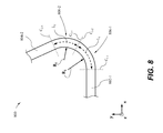
- FIG. 8 another exemplary waveguide 800 , similar to the waveguide 700 , includes first and second adjacent bends or curved portions 806 - 1 , 806 - 2 .
- a radius of curvature R 1 of the bend 806 - 1 is different than the radius of curvature R 2 of the bend 806 - 2 .
- Waveguide 800 includes a straight portion 802 - 1 which couples to the input geometric plane C 1 - 1 of the bend 806 - 1 .
- Bend 806 - 1 includes an arc length L 1 and ends in an output geometric plane C 1-2 , which also acts as the input geometric plane C 2-1 of bend 806 - 2 .
- Bend 806 - 2 includes an arc length L 2 , ending in the output geometric plane C 2-2 which couples to a straight portion 804 - 2 . While the bends 806 - 1 , 806 - 2 are depicted as two separate bends or curved portions, bends 806 - 1 , 806 - 2 may be referred to as a single bend 806 having geometric dimensions commensurate with bens 806 - 1 and 806 - 2 .
- the waveguide 800 may include one or more additional straight portions, one of which may be positioned between the bends or curved portions 806 - 1 , 806 - 2 , coupling the output geometric plane C 1-2 with the input geometric plane C 2-1 .
- the bends 806 - 1 , 806 - 2 of waveguide 800 may individually preserve the orientation of the polarization state of an optical signal propagating through the waveguide 800 , e.g. the orientation of the polarization state at the input geometric plane C 1-1 , C 2-1 being similar to the orientation of the polarization state at the corresponding output geometric plane C 1-2 , C 2-2 , respectively.
Landscapes
- Physics & Mathematics (AREA)
- General Physics & Mathematics (AREA)
- Optics & Photonics (AREA)
- Engineering & Computer Science (AREA)
- Microelectronics & Electronic Packaging (AREA)
- Optical Integrated Circuits (AREA)
Abstract
Description
L=2N*Lb (1)
where Lb is a beat length and N is an integer. As mentioned above, each of the two eigenmodes propagates at slightly different velocities in the
where B1 and B1 are the propagation constants of the first and second eigenmodes, respectively. Substituting Lb of equation (2) into equation (1) above results in:
As compared to
Finally,
As depicted in
Claims (7)
Priority Applications (1)
| Application Number | Priority Date | Filing Date | Title |
|---|---|---|---|
| US12/828,129 US8634684B2 (en) | 2010-06-30 | 2010-06-30 | Anti-resonant waveguide bends |
Applications Claiming Priority (1)
| Application Number | Priority Date | Filing Date | Title |
|---|---|---|---|
| US12/828,129 US8634684B2 (en) | 2010-06-30 | 2010-06-30 | Anti-resonant waveguide bends |
Publications (2)
| Publication Number | Publication Date |
|---|---|
| US20120002920A1 US20120002920A1 (en) | 2012-01-05 |
| US8634684B2 true US8634684B2 (en) | 2014-01-21 |
Family
ID=45399767
Family Applications (1)
| Application Number | Title | Priority Date | Filing Date |
|---|---|---|---|
| US12/828,129 Expired - Fee Related US8634684B2 (en) | 2010-06-30 | 2010-06-30 | Anti-resonant waveguide bends |
Country Status (1)
| Country | Link |
|---|---|
| US (1) | US8634684B2 (en) |
Cited By (2)
| Publication number | Priority date | Publication date | Assignee | Title |
|---|---|---|---|---|
| US20200310028A1 (en) * | 2019-04-01 | 2020-10-01 | Lumentum Operations Llc | Curved waveguide configuration |
| US20240094468A1 (en) * | 2022-09-19 | 2024-03-21 | Apple Inc. | Photonic Passive Delay Lines with Reduced Parasitic Losses |
Citations (3)
| Publication number | Priority date | Publication date | Assignee | Title |
|---|---|---|---|---|
| US20010024547A1 (en) * | 2000-02-17 | 2001-09-27 | Wei-Ping Huang | Strongly confined polarization-independent single-mode optical ridge waveguide |
| US6546161B2 (en) * | 2000-01-21 | 2003-04-08 | Nippon Telegraph And Telephone Corporation | No polarization dependent waveguide type optical circuit |
| US20110317960A1 (en) * | 2009-01-05 | 2011-12-29 | Georgetown University | Direct coupling of optical slot waveguide to another optical waveguide |
-
2010
- 2010-06-30 US US12/828,129 patent/US8634684B2/en not_active Expired - Fee Related
Patent Citations (3)
| Publication number | Priority date | Publication date | Assignee | Title |
|---|---|---|---|---|
| US6546161B2 (en) * | 2000-01-21 | 2003-04-08 | Nippon Telegraph And Telephone Corporation | No polarization dependent waveguide type optical circuit |
| US20010024547A1 (en) * | 2000-02-17 | 2001-09-27 | Wei-Ping Huang | Strongly confined polarization-independent single-mode optical ridge waveguide |
| US20110317960A1 (en) * | 2009-01-05 | 2011-12-29 | Georgetown University | Direct coupling of optical slot waveguide to another optical waveguide |
Cited By (3)
| Publication number | Priority date | Publication date | Assignee | Title |
|---|---|---|---|---|
| US20200310028A1 (en) * | 2019-04-01 | 2020-10-01 | Lumentum Operations Llc | Curved waveguide configuration |
| US11048042B2 (en) * | 2019-04-01 | 2021-06-29 | Lumentum Operations Llc | Curved waveguide configuration to suppress mode conversion |
| US20240094468A1 (en) * | 2022-09-19 | 2024-03-21 | Apple Inc. | Photonic Passive Delay Lines with Reduced Parasitic Losses |
Also Published As
| Publication number | Publication date |
|---|---|
| US20120002920A1 (en) | 2012-01-05 |
Similar Documents
| Publication | Publication Date | Title |
|---|---|---|
| US10591802B2 (en) | On-chip optical phased array using a serial grating antenna design | |
| US7006732B2 (en) | Polarization splitting grating couplers | |
| CN109564326B (en) | Single-mode waveguide with adiabatic bends | |
| US8494314B2 (en) | Fabrication tolerant polarization converter | |
| US8761562B2 (en) | Multicore fiber and core placement method for multicore fiber | |
| JP6631524B2 (en) | Optical circuit element and method of configuring optical circuit element | |
| JP5561305B2 (en) | Optical element | |
| CN105378526A (en) | Polarization conversion element | |
| CN111819480A (en) | Photonic devices for converting light modes of light beams | |
| US7215854B2 (en) | Low-loss optical waveguide crossovers using an out-of-plane waveguide | |
| US7760974B2 (en) | Silicon arrayed waveguide grating device for reducing effective refractive index variation of optical waveguide according to temperature | |
| JP2014041252A (en) | Optical waveguide element | |
| JP5702757B2 (en) | Optical waveguide device | |
| US8634684B2 (en) | Anti-resonant waveguide bends | |
| CN107688210B (en) | Optical waveguide interferometer and method for manufacturing optical waveguide interferometer | |
| JP2023040871A (en) | Optical waveguide device and optical integrated circuit | |
| JP6397862B2 (en) | Optical waveguide device | |
| KR101725637B1 (en) | Optical signal coupling appratus and method using grating-to-grating coupler having bandwidth performance enhancement | |
| GB2239715A (en) | Integrated optical device | |
| US11156777B2 (en) | Method for producing a polarization converter, polarization converter and polarization converter element | |
| JP6530061B2 (en) | Grating coupler | |
| CN118057224A (en) | Optical component with adjacent metamaterial structures | |
| JP2006508383A (en) | Optical demultiplexing components with low polarization sensitivity and large processing tolerance | |
| US20240094468A1 (en) | Photonic Passive Delay Lines with Reduced Parasitic Losses | |
| CN121995576A (en) | Polarization beam splitter-rotator |
Legal Events
| Date | Code | Title | Description |
|---|---|---|---|
| AS | Assignment |
Owner name: INFINERA CORPORATION, CALIFORNIA Free format text: ASSIGNMENT OF ASSIGNORS INTEREST;ASSIGNORS:LITTLE, BRENT E.;EVANS, PETER W.;SIGNING DATES FROM 20100818 TO 20100910;REEL/FRAME:024995/0307 |
|
| STCF | Information on status: patent grant |
Free format text: PATENTED CASE |
|
| FPAY | Fee payment |
Year of fee payment: 4 |
|
| MAFP | Maintenance fee payment |
Free format text: PAYMENT OF MAINTENANCE FEE, 8TH YEAR, LARGE ENTITY (ORIGINAL EVENT CODE: M1552); ENTITY STATUS OF PATENT OWNER: LARGE ENTITY Year of fee payment: 8 |
|
| FEPP | Fee payment procedure |
Free format text: MAINTENANCE FEE REMINDER MAILED (ORIGINAL EVENT CODE: REM.); ENTITY STATUS OF PATENT OWNER: LARGE ENTITY |
|
| LAPS | Lapse for failure to pay maintenance fees |
Free format text: PATENT EXPIRED FOR FAILURE TO PAY MAINTENANCE FEES (ORIGINAL EVENT CODE: EXP.); ENTITY STATUS OF PATENT OWNER: LARGE ENTITY |
|
| STCH | Information on status: patent discontinuation |
Free format text: PATENT EXPIRED DUE TO NONPAYMENT OF MAINTENANCE FEES UNDER 37 CFR 1.362 |
|
| FP | Lapsed due to failure to pay maintenance fee |
Effective date: 20260121 |