US8625109B2 - Method of determining an overlap distance of an optical head and digital exposure device using the method - Google Patents
Method of determining an overlap distance of an optical head and digital exposure device using the method Download PDFInfo
- Publication number
- US8625109B2 US8625109B2 US12/902,745 US90274510A US8625109B2 US 8625109 B2 US8625109 B2 US 8625109B2 US 90274510 A US90274510 A US 90274510A US 8625109 B2 US8625109 B2 US 8625109B2
- Authority
- US
- United States
- Prior art keywords
- area
- light
- substrate
- light amount
- optical head
- Prior art date
- Legal status (The legal status is an assumption and is not a legal conclusion. Google has not performed a legal analysis and makes no representation as to the accuracy of the status listed.)
- Active, expires
Links
Images


Classifications
-
- G—PHYSICS
- G01—MEASURING; TESTING
- G01B—MEASURING LENGTH, THICKNESS OR SIMILAR LINEAR DIMENSIONS; MEASURING ANGLES; MEASURING AREAS; MEASURING IRREGULARITIES OF SURFACES OR CONTOURS
- G01B11/00—Measuring arrangements characterised by the use of optical techniques
- G01B11/14—Measuring arrangements characterised by the use of optical techniques for measuring distance or clearance between spaced objects or spaced apertures
-
- G—PHYSICS
- G03—PHOTOGRAPHY; CINEMATOGRAPHY; ANALOGOUS TECHNIQUES USING WAVES OTHER THAN OPTICAL WAVES; ELECTROGRAPHY; HOLOGRAPHY
- G03F—PHOTOMECHANICAL PRODUCTION OF TEXTURED OR PATTERNED SURFACES, e.g. FOR PRINTING, FOR PROCESSING OF SEMICONDUCTOR DEVICES; MATERIALS THEREFOR; ORIGINALS THEREFOR; APPARATUS SPECIALLY ADAPTED THEREFOR
- G03F7/00—Photomechanical, e.g. photolithographic, production of textured or patterned surfaces, e.g. printing surfaces; Materials therefor, e.g. comprising photoresists; Apparatus specially adapted therefor
- G03F7/70—Microphotolithographic exposure; Apparatus therefor
- G03F7/70483—Information management; Active and passive control; Testing; Wafer monitoring, e.g. pattern monitoring
- G03F7/7055—Exposure light control in all parts of the microlithographic apparatus, e.g. pulse length control or light interruption
-
- G—PHYSICS
- G03—PHOTOGRAPHY; CINEMATOGRAPHY; ANALOGOUS TECHNIQUES USING WAVES OTHER THAN OPTICAL WAVES; ELECTROGRAPHY; HOLOGRAPHY
- G03F—PHOTOMECHANICAL PRODUCTION OF TEXTURED OR PATTERNED SURFACES, e.g. FOR PRINTING, FOR PROCESSING OF SEMICONDUCTOR DEVICES; MATERIALS THEREFOR; ORIGINALS THEREFOR; APPARATUS SPECIALLY ADAPTED THEREFOR
- G03F7/00—Photomechanical, e.g. photolithographic, production of textured or patterned surfaces, e.g. printing surfaces; Materials therefor, e.g. comprising photoresists; Apparatus specially adapted therefor
- G03F7/70—Microphotolithographic exposure; Apparatus therefor
- G03F7/70058—Mask illumination systems
- G03F7/70075—Homogenization of illumination intensity in the mask plane by using an integrator, e.g. fly's eye lens, facet mirror or glass rod, by using a diffusing optical element or by beam deflection
-
- G—PHYSICS
- G03—PHOTOGRAPHY; CINEMATOGRAPHY; ANALOGOUS TECHNIQUES USING WAVES OTHER THAN OPTICAL WAVES; ELECTROGRAPHY; HOLOGRAPHY
- G03F—PHOTOMECHANICAL PRODUCTION OF TEXTURED OR PATTERNED SURFACES, e.g. FOR PRINTING, FOR PROCESSING OF SEMICONDUCTOR DEVICES; MATERIALS THEREFOR; ORIGINALS THEREFOR; APPARATUS SPECIALLY ADAPTED THEREFOR
- G03F7/00—Photomechanical, e.g. photolithographic, production of textured or patterned surfaces, e.g. printing surfaces; Materials therefor, e.g. comprising photoresists; Apparatus specially adapted therefor
- G03F7/70—Microphotolithographic exposure; Apparatus therefor
- G03F7/70058—Mask illumination systems
- G03F7/70191—Optical correction elements, filters or phase plates for controlling intensity, wavelength, polarisation, phase or the like
-
- G—PHYSICS
- G03—PHOTOGRAPHY; CINEMATOGRAPHY; ANALOGOUS TECHNIQUES USING WAVES OTHER THAN OPTICAL WAVES; ELECTROGRAPHY; HOLOGRAPHY
- G03F—PHOTOMECHANICAL PRODUCTION OF TEXTURED OR PATTERNED SURFACES, e.g. FOR PRINTING, FOR PROCESSING OF SEMICONDUCTOR DEVICES; MATERIALS THEREFOR; ORIGINALS THEREFOR; APPARATUS SPECIALLY ADAPTED THEREFOR
- G03F7/00—Photomechanical, e.g. photolithographic, production of textured or patterned surfaces, e.g. printing surfaces; Materials therefor, e.g. comprising photoresists; Apparatus specially adapted therefor
- G03F7/70—Microphotolithographic exposure; Apparatus therefor
- G03F7/70216—Mask projection systems
- G03F7/70283—Mask effects on the imaging process
- G03F7/70291—Addressable masks, e.g. spatial light modulators [SLMs], digital micro-mirror devices [DMDs] or liquid crystal display [LCD] patterning devices
-
- G—PHYSICS
- G03—PHOTOGRAPHY; CINEMATOGRAPHY; ANALOGOUS TECHNIQUES USING WAVES OTHER THAN OPTICAL WAVES; ELECTROGRAPHY; HOLOGRAPHY
- G03F—PHOTOMECHANICAL PRODUCTION OF TEXTURED OR PATTERNED SURFACES, e.g. FOR PRINTING, FOR PROCESSING OF SEMICONDUCTOR DEVICES; MATERIALS THEREFOR; ORIGINALS THEREFOR; APPARATUS SPECIALLY ADAPTED THEREFOR
- G03F7/00—Photomechanical, e.g. photolithographic, production of textured or patterned surfaces, e.g. printing surfaces; Materials therefor, e.g. comprising photoresists; Apparatus specially adapted therefor
- G03F7/70—Microphotolithographic exposure; Apparatus therefor
- G03F7/70216—Mask projection systems
- G03F7/70308—Optical correction elements, filters or phase plates for manipulating imaging light, e.g. intensity, wavelength, polarisation, phase or image shift
-
- G—PHYSICS
- G03—PHOTOGRAPHY; CINEMATOGRAPHY; ANALOGOUS TECHNIQUES USING WAVES OTHER THAN OPTICAL WAVES; ELECTROGRAPHY; HOLOGRAPHY
- G03F—PHOTOMECHANICAL PRODUCTION OF TEXTURED OR PATTERNED SURFACES, e.g. FOR PRINTING, FOR PROCESSING OF SEMICONDUCTOR DEVICES; MATERIALS THEREFOR; ORIGINALS THEREFOR; APPARATUS SPECIALLY ADAPTED THEREFOR
- G03F7/00—Photomechanical, e.g. photolithographic, production of textured or patterned surfaces, e.g. printing surfaces; Materials therefor, e.g. comprising photoresists; Apparatus specially adapted therefor
- G03F7/70—Microphotolithographic exposure; Apparatus therefor
- G03F7/70425—Imaging strategies, e.g. for increasing throughput or resolution, printing product fields larger than the image field or compensating lithography- or non-lithography errors, e.g. proximity correction, mix-and-match, stitching or double patterning
- G03F7/70475—Stitching, i.e. connecting image fields to produce a device field, the field occupied by a device such as a memory chip, processor chip, CCD, flat panel display
-
- G—PHYSICS
- G03—PHOTOGRAPHY; CINEMATOGRAPHY; ANALOGOUS TECHNIQUES USING WAVES OTHER THAN OPTICAL WAVES; ELECTROGRAPHY; HOLOGRAPHY
- G03F—PHOTOMECHANICAL PRODUCTION OF TEXTURED OR PATTERNED SURFACES, e.g. FOR PRINTING, FOR PROCESSING OF SEMICONDUCTOR DEVICES; MATERIALS THEREFOR; ORIGINALS THEREFOR; APPARATUS SPECIALLY ADAPTED THEREFOR
- G03F7/00—Photomechanical, e.g. photolithographic, production of textured or patterned surfaces, e.g. printing surfaces; Materials therefor, e.g. comprising photoresists; Apparatus specially adapted therefor
- G03F7/70—Microphotolithographic exposure; Apparatus therefor
- G03F7/708—Construction of apparatus, e.g. environment aspects, hygiene aspects or materials
- G03F7/70858—Environment aspects, e.g. pressure of beam-path gas, temperature
- G03F7/70883—Environment aspects, e.g. pressure of beam-path gas, temperature of optical system
Definitions
- Exemplary embodiments of the present invention relate to an apparatus and a method for determining an overlap distance of an optical head. More particularly, exemplary embodiments of the present invention relate to a digital exposure device and a method for determining an overlap distance of an optical head used for a digital exposure.
- the metal pattern may be formed using a mask having a design of a metal pattern which may be disposed on the photoresist layer.
- the photoresist layer can be exposed and developed by providing light to an upper portion of the mask to form a photoresist pattern in which the design of the mask may be reflected.
- the metal layer can be etched by using the photoresist pattern serving as an etch stop layer so that the metal pattern may be formed.
- a display substrate includes a plurality of metal patterns
- a plurality of masks by the number of the metal patterns may be required due to different patterns.
- the design of the mask may also be required to be changed so that a mask may be re-produced. Since a reproduction cost of the mask is relatively high, reproducing the mask may increase the manufacturing cost of a display substrate.
- an approach has been introduced to an exposure device capable of providing a substrate with beams without using a mask.
- the beams may be activated or inactivated to selectively be provided to the substrate so that photoresist patterns dependent on a shape can be defined by the activation or inactivation of the beams. Since an area covered by light provided from the exposure device is limited, the exposure device or the substrate is moved to scan in several times when a photoresist pattern is formed on a large-sized substrate by using the exposure device. In this way, the substrate may fully be exposed by the exposure device.
- an overlapped area may be generated.
- the overlapped area of the substrate can be exposed by the exposure device at least more than two times so that unnecessary exposures in terms of generating patterns can not only be a burden to manufacturing a display substrate but adversely affect a manufacturing yield since a uniformity of the photoresist pattern may be decreased.
- Exemplary embodiments of the present invention provide an apparatus and a method for determining an overlap distance of an optical head capable of uniformizing an overlapped area.
- Exemplary embodiments of the present invention provide a digital exposure device to determine an overlap distance of an optical head.
- Exemplary embodiments of the present invention disclose a method for determining an overlap distance for direct patterning using an optical lithography.
- the method includes detecting light amount distributions and positions of each light spot generated from an optical head to a substrate, the substrate comprising a first area and a second area.
- the method also includes generating a compensation model of each of the light spots by applying a Gaussian distribution function to the respective positions of the light spots and light amount distributions of the light spots.
- the method includes calculating a first accumulated light amount corresponding to each light spot of the first area of the substrate, the optical head being first scanned along a first direction of the substrate using the compensation model.
- the method also includes calculating a second accumulated light amount corresponding to each light spot of the second area overlapped with the first area, the overlap area being occurred when the optical head second scanned along the first direction after being moved in a second direction by a first distance using the compensation model.
- the method includes determining an overlap distance according to a uniformity of the summation of the first accumulated light amount and the second accumulated light amount.
- Exemplary embodiments of the present invention disclose an optical device.
- the optical device includes an optical head comprising a light modulation element to convert light into light comprising plural light paths, the optical head to generate a plurality of laser beams to a substrate by using the light modulation element.
- the optical device also includes a measuring part to detect positions and light amount distribution of each of light spots incident on a substrate.
- the optical device includes a calculating part to calculate a compensation model of each of the light spots by applying Gaussian distribution to the detected positions and the light amount distributions.
- the calculating part is configured to calculate a first accumulated light amount corresponding to the respective positions of the first area of the substrate when the optical head is scanned along a first direction of the substrate using the compensation model.
- the calculating part is also configured to calculate a second accumulated light amount corresponding to the respective positions of the second area overlapped with positions of the first area.
- the overlapped area is occurred when the optical head is second scanned along the first direction after being moved in a second direction by a first distance using the compensation model.
- An overlap distance is determined according to a uniformity of summations of the first accumulated light amounts and the second accumulated light amounts.
- Exemplary embodiments of the present invention disclose an apparatus.
- the apparatus includes a compensation part configured to detect an overlap area in a direct patterning using an optical lithography to compensate errors associated with the overlap area.
- the overlap area is determined by measuring positions and light amount of each light spot distributed on a substrate and the distribution is calculated by applying a Gaussian distribution to the measured positions and light amount distribution.
- the substrate comprises a first area comprising a plurality of sectors and a second area comprising a plurality of sectors, and a first accumulated amount is measured corresponding to the respective sectors of the first area in response to detection of a optical head scanning in a first direction and a second accumulated amount is measured corresponding to the respective sectors of the second area overlapped with the sectors of the first area in response to detection of a optical head is second scanned in the first direction after being moved in a second direction by a first distance.
- a control part is configured to control of a mirror arranged in matrix, the control being associated with selectively activating and inactivating light incidence on the substrate. The mirror is controlled by the overlap area and the overlap area is determined according to a uniformity of the summation of the first accumulated light amount and the second accumulated light amount.
- Exemplary embodiments of the present invention disclose a method.
- the method includes detecting light amount distribution and each position of light spots generated from an optical head for direct patterning on a substrate, the light spots comprising a first area and a second area.
- the method also includes determining a first accumulated light amount corresponding to each light spot of the first area of the substrate, the optical head being scanned along a first direction of the substrate using a compensation model, wherein the compensation model is provided by applying Gaussian distribution function to the respective positions of the light spots and the light amount distributions.
- the method also includes determining, using the compensation model, a second accumulated light amount corresponding to each light spot of the second area overlapped with the first area the overlap area being occurred if the optical head is second scanned along the first direction after being moved in a second direction by a first distance.
- the method also includes controlling a stepping distance of the optical head to generate uniform light incidence with respect to the overlap area based on the determination of the first and second accumulated light amount.
- FIG. 1 is a diagram of a digital exposure device capable of determining an overlap distance of an optical head according to exemplary embodiments of the present invention.
- FIG. 2 is a diagram showing an exposure of a substrate by using an optical head of FIG. 1 .
- FIG. 3 is a flowchart of a process for determining an overlap distance by the obtaining part of FIG. 1 .
- FIG. 4A is diagram showing a position of a light spot of FIG. 1 .
- FIG. 4B is a diagram showing a light amount distribution of the light spot of FIG. 1 .
- FIG. 5 is a diagram illustrating Gaussian distribution function of a light spot provided to a substrate by the optical head of FIG. 1 .
- FIG. 6 is a flow chart of a process for measuring and calculating light amount associated with a driving method of the overlap distance obtaining part of FIG. 3 .
- FIG. 7A , FIG. 7B and FIG. 7C are diagrams showing a second calculating part and a third calculating part of FIG. 3 .
- FIG. 8A , FIG. 8B , FIG. 8C and FIG. 8D are graphs illustrating a uniformity of accumulated exposure light amount that is calculated in accordance with exemplary embodiments of the present invention.
- FIG. 9 is a diagram of hardware that can be used to implement various embodiments of the invention.
- spatially relative terms such as “beneath,” “below,” “lower,” “above,” “upper” may be used herein for easy understanding of illustration of one element or feature's relationship to another element(s) or feature(s) as illustrated in the figures. It is understood that the spatially relative terms may be intended to encompass different orientations of the device in use or operation in addition to the orientation depicted in the figures. For example, if the device in the figures is turned over, elements described as “below” or “beneath” other elements or features may be oriented “above” the other elements or features. Thus, the exemplary term “below” may encompass both an orientation of above and below. According to an exemplary configuration, a device may be otherwise oriented to a direction (e.g., rotated 90 degrees or at other orientations) and the spatially relative terms used herein associated with other elements and/or features may be interpreted accordingly.
- Exemplary embodiments of the invention are described herein with reference to cross-sectional illustrations that are schematic illustrations of idealized exemplary embodiments (and intermediate structures) of the present invention. As such, various exemplary embodiments are illustrated by way of examples, and not by way of limitation, for example, variations due to manufacturing techniques and/or tolerances may be expected. Thus, illustrated exemplary embodiments of the present invention should not be construed as limited to the particular shapes of regions illustrated herein but may be construed to include deviations in shapes that may be resulted from manufacturing configurations. For example, an implanted region illustrated as a rectangular shape may, typically, have rounded or curved features and/or a gradient of implant concentration at its edges rather than a binary change from implanted to non-implanted region.
- a buried region formed by implantation may result in some implantation in the region between the buried region and the surface through which the implantation takes place.
- the regions illustrated in the figures are illustrative in nature and their shapes are not intended to restrict the actual shape of a region of a device and are not intended to limit the scope of the present invention.
- FIG. 1 is a diagram of a digital exposure device capable of determining an overlap distance of an optical head according to exemplary embodiments of the present invention.
- the digital exposure device may include an optical head 100 , a light source 200 , a mirror control part 310 , a stepping control part 320 and an overlap distance obtaining part 330 .
- the optical head 100 may include a light modulating element 110 , a splitter 120 and an optical system 130 .
- the optical head 100 may be connected to the light source 200 , the mirror control part 310 and the stepping control part 320 .
- the light modulating element may include a digital micro-mirror device (“DMD”) 110 .
- the light source 200 may be connected to the splitter 120 to provide the splitter 120 with a first light L 1 emitted from the light source 200 .
- the splitter 120 can receive the first light L 1 to provide a second light L 2 to the DMD 110 by converting a path of the first light L 1 .
- the DMD 110 may reflect the second light L 2 to emit a plurality of third lights L 3 onto the optical system 130 .
- the DMD 110 may include a plurality of micro-mirrors M.
- the micro-mirrors M may be arranged in an ‘m ⁇ n’ matrix.
- Each of the ‘m ⁇ n’ micro-mirrors M may reflect the second light L 2 to provide the optical system 130 with ‘m ⁇ n’ third lights L 3 .
- the DMD 110 may selectively reflect the second light L 2 onto a substrate SU which may be disposed on a stage 400 based on an image data which can be transferred thereto.
- the mirror control part 310 may activate or inactivate each of the micro-mirrors M based on the image data.
- the mirror control part 310 can output a signal controlling an activation or inactivation of the micro-mirrors M to each of the micro-mirrors M.
- each of the micro-mirrors M may reflect the second light L 2 onto the optical system 130 .
- portions of the micro-mirrors M receive an activation data from the mirror control part 310 , corresponding micro-mirrors reflect the second light L 2 onto the optical system 130 .
- the remaining micro-mirrors M receive an inactivation data from the mirror control part 310 , the remaining micro-mirrors M do not reflect the second light L 2 .
- the optical system 130 may include a plurality of lenses.
- the optical system 130 may condense the third lights L 3 provided from the DMD 110 , and may emit a fourth light L 4 onto the stage 400 by adjusting a resolution of the condensed lights.
- the fourth lights L 4 may correspond to a plurality of laser beams which is provided to the stage 400 by the optical head 100 .
- the number of laser beams can be ‘m ⁇ n.’
- the number of laser beams may substantially be equal to the number of activated micro-mirrors M.
- the laser beams may be provided on the substrate SU disposed on the stage 400 as a plurality of light spots 500 .
- the light spots 500 may be defined as an exposure area on which the laser beams are actually irradiated.
- the substrate SU receives ‘m ⁇ n’ light spots 500 being substantially equal to the number of micro-mirrors M.
- the optical head 100 may provide the substrate SU with the light spots 500 of an ‘m ⁇ n’ matrix at a state that the optical head 100 and the stage 400 are stopped.
- an area of the substrate SU between the light spots 500 adjacent to each other may be a non-exposure area where the laser beam may not be provided thereto.
- FIG. 2 is a diagram showing an exposure of a substrate by using an optical head of FIG. 1 .
- portions of the micro-mirrors M may receive an activation data from the mirror control part 310 , and the remaining of the micro-mirrors M may receive an inactivation data from the mirror control part 310 .
- the substrate SU can receive the light spots as many as the number of micro-mirrors M corresponding to the activation data. Therefore, a predetermined area of the substrate SU may selectively be exposed without a mask having a design of the image data between the optical head 100 and the substrate SU.
- the micro-mirrors M receiving the inactivation data may not provide the substrate SU with light.
- the micro-mirrors M receiving the inactivation data are denoted as “a virtual spot,” and a “virtual spot” represented by a reference numeral “ 520 .”
- exposing the substrate SU using the optical head 100 is for exposing a photoresist payer PR formed on the substrate SU.
- the term “an exposure of a substrate” may include the term “an exposure of a photoresist layer.”
- the substrate SU disposed on the stage 400 may be scanned by the optical head 100 .
- the angle of incline of optical head 100 disposed on the stage 400 may be at a predetermined angle ‘ ⁇ ’ with respect to the substrate SU.
- the substrate SU may be exposed by the optical head 100 .
- the stage 400 may be moved in the first direction D 1 at a state that the stage 400 may be inclined with respect to the optical head 100 so that the substrate SU may be exposed by the optical head 100 .
- the straight line area may sequentially receive light spots 500 provided by the micro-mirrors M of a first row, light spots 500 provided by the micro-mirrors M of a second row, and light spots 500 provided by the micro-mirrors M of a third row.
- the ‘m ⁇ n’ light spots 500 overlapped along the second direction D 2 may be irradiated into the straight line area.
- the ‘m ⁇ n’ light spots 500 may be irradiated onto each of the straight line areas.
- the ‘m ⁇ n’ micro-mirrors M can provide light spots 500 spaced apart from each other to the substrate SU. However, since the stage 400 is moved in an inclined state in which the optical head 100 is inclined with respect to the stage 400 by a predetermined angle, the substrate SU corresponding to a scanned area of the optical head 100 may be exposed by the optical head 100 without an area where the substrate may not be exposed.
- the optical head 100 When the optical head 100 irradiates lights onto the substrate SU in a state that the optical head 100 is not inclined with respect to the stage 400 , for example, the optical head 100 is inclined by a predetermined angle “ ⁇ ” less than about 0.1 with respect to the stage 400 , lights may be not irradiated to areas of the substrate SU corresponding to an area between the light spots 500 adjacent to each other even though the optical head 100 is moved in the first direction D 1 . In this example, a continuous line pattern or a continuous area may not be exposed.
- a predetermined angle “ ⁇ ” is more than about 0.5, a distance between the light spots 500 provided by the micro-mirrors M of the first row and the light spots 500 provided by the micro-mirrors M of the second row may be increased at a straight line area of the stage 400 .
- pattern quality such as a line edge roughness (“LER”) may be deteriorated. Therefore, in order to provide a light amount of an optimum level to the whole substrate SU by using the optical head 100 , the predetermined angle “ ⁇ ” may be, for example, no less than about 0.1 to no more than about 0.5. (e.g., 0.1 ⁇ 0.5)
- the image data may determine a coordinate of an area which may be exposed on the substrate SU.
- the image data may be reflected to active or inactive data of the micro-mirrors M.
- the micro-mirrors M may receive an activation data to provide the light spot 500 to the substrate SU. Since the micro-mirror M which does not correspond to the coordinate receives an inactivation data, the substrate SU can only receive the virtual spot 520 .
- the substrate SU corresponding to an area on which the micro-mirrors M receiving the inactivation data is scanned may not be exposed.
- a predetermined area of the substrate SU may selectively be exposed without a mask having a design in which the image data may be reflected between the optical head 100 and the substrate SU.
- the stepping control part 320 may be connected to the optical head 100 to move the optical head 100 in one direction. Since a width of the optical head 100 is limited, lights may be not provided to an entire surface of the substrate SU by using one optical head 100 .
- the substrate SU may be divided into a plurality of unit areas which are extended in the first direction D 1 and are arranged in the second direction D 2 , and the substrate SU is scanned for plural times by using the optical head 100 .
- the optical head 100 may firstly scan a first unit area A 1 (refer to FIG. 7A ) of the substrate SU, and then secondly scan a second unit area A 2 (refer to FIG.
- the stepping control part 320 may control that the optical head 100 is moved by a predetermined interval in the second direction D 2 .
- a movement of the optical head 100 in the second direction D 2 with respect to the substrate SU can be defined as “a stepping,” and a predetermined interval by which the optical head 100 is moved can be defined as “a stepping distance.”
- the overlap distance obtaining part 330 may determine an overlapped area A 3 (refer to FIG. 7A ) of the substrate SU and an overlap distance that is a width of the overlapped area A 3 . Since the optical head 100 firstly and secondly scans the substrate SU in a state in which the substrate SU is inclined with the optical head 100 by a predetermined angle, a boundary area between the first unit area A 1 and the second unit area A 2 is an area that can be formed to be exposed without a non-exposed area. The stepping distance may be determined based on the overlapped area A 3 and the overlap distance.
- the overlap distance obtaining part 330 , the overlapped area A 2 and the overlap distance will be described below in detail with reference to FIG. 3 , FIG. 6 , FIG. 7A , FIG. 7B and FIG. 7C .
- FIG. 3 is a flowchart of a process for determining an overlap distance obtaining part of FIG. 1 .
- the overlap distance obtaining part 330 may include a measuring part 331 , a first calculating part 333 , a second calculating part 334 a , a third calculating part 334 b and a determining part 337 .
- the measuring part 331 may measure a position and a light amount distribution of each of the light spots 500 provided to substrate SU from the optical head 100 .
- the micro-mirrors M of the optical head 100 are theoretically designed to have an ‘m ⁇ n’ square matrix, but alternative exemplary embodiments may be implemented.
- a matrix forming the micro-mirrors M may not be a perfect square shape.
- the substrate SU may not receive a light spot having a shape identical to the laser beam. A refraction of a light spot can be generated due to air generated in a process that the laser beam irradiated from the optical head 100 is reached to the substrate SU so that the positions and light amount distributions of ideal light spots and the positions and light amount distributions of the light spots 500 actually being measured may be different from each other.
- the measuring part 331 may measure the position and light amount distribution of the light spots 500 so that the overlap distance obtaining part 330 may reflect the position and light amount distribution of the light spots 500 to determine the overlap distance.
- the measuring part 331 may include an optical sensor disposed on the substrate SU.
- the first calculating part 333 may use Gaussian distribution function to the position and light amount distribution of the light spots 500 measured by the measuring part 331 to calculate compensation models of each of the light spots 500 .
- the second calculating part 334 a may calculate a first accumulated light amount corresponding to each of first sub-areas of the substrate SU if the optical head 100 is scanned in the first direction D 1 by using the compensation model. For example, the first accumulated light amount may be calculated based on the compensation model obtained by the first calculating part 334 a not based on actually performing an exposure process to the substrate SU by using the optical head 100 .
- the third calculating part 334 b may calculate a second accumulated light amount corresponding to each of second sub-areas including second areas D 21 , D 22 and D 23 (refer to FIG. 7C ) corresponding to first areas D 11 , D 12 and D 13 (refer to FIG. 7C ) of the first sub-areas if the optical head 100 moved by about first distance in the second direction D 2 by using the compensation model is scanned along the first direction D 1 .
- the second accumulated light amount may be calculated based on the compensation model obtained by the first calculating part 334 a not a calculation by actually performing an exposure process.
- the determining part 337 may determine the overlap distance in accordance with a uniformity of summations of the second accumulated light amounts respectively corresponding to the second areas D 21 , D 22 and D 23 and the first accumulated light amounts respectively corresponding to the first areas D 11 , D 12 and D 13 respectively being overlapped with the second areas D 21 , D 22 and D 23 .
- the stepping distance may be determined by a moving distance of the optical head 100 if the overlap distance is calculated. If the summations of the first accumulated light and the second accumulated light are determined as uniform, the overlap distance can be determined.
- the optical head 100 may be moved by a second distance to calculate an accumulated light amount by the third calculating part 334 b with respect to another overlapped area, and then the determining part 337 may determine whether the summations are uniform or non-uniform to determine the overlap distance.
- a position and a light amount distribution of the light spots are measured by the measuring part 331 and the first calculating part 333 , and Gaussian distribution function is applied to the position and the light amount distribution to calculate the compensation model.
- FIG. 4A is a diagram showing a position of a light spot of FIG. 1
- FIG. 4B is a diagram showing a light amount distribution of the light spot of FIG. 1 .
- an ideal light spot may be disposed at a first position 112 on the substrate SU.
- actual light spots 500 may be positioned at a second position 114 which is not matched to the first position 112 on the substrate SU.
- the overlap distance obtaining part 330 can measure the second position 114 that is an actual position of the light spots 500 .
- the light amount distribution may not be uniform in a single light spot 500 .
- the light spot 500 may be classified into a high area HA in which an energy is condensed to have a high energy and a low area ‘LA’ which has a lower energy than the high area ‘HA.’
- light amount distributions may be different from one another in accordance with areas, and light amount distributions of the different light spots 500 may be different from one another.
- the measuring part 331 may measure an actual light amount distribution of the light spots 500 .
- FIG. 5 is a diagram illustrating Gaussian distribution function of a light spot provided to a substrate by the optical head of FIG. 1 .
- the light spots 500 may have a bell shape 510 in a three-dimension.
- a cross-sectional view of the light spots 500 may depict Gaussian distribution function.
- An energy may be the highest in a center portion of the light spots 500 , and the energy may gradually be decreased as it goes further away from the center portion thereof to be closer toward an edge portion thereof.
- the light spots 500 may be overlapped through the scanning process so that total summations of the light amounts corresponding to the scanned area may be determined.
- the Gaussian distribution function may be applied to a position and a light amount distribution of the light spots 500 so that each compensation model of the light spots 500 may be calculated.
- the compensation model may have a similar shape with an actual light spot 500 .
- FIG. 6 is a flow chart of a process for measuring and calculating light amount associated with a driving method of the overlap distance obtaining part of FIG. 3 .
- step S 10 positions and light amount distribution of each of the light spots 500 may be measured.
- the measuring of the positions and light amount distribution may be performed by the measuring part 331 of the digital exposure device.
- step S 20 Gaussian distribution function is applied to the position and the light amount distribution to calculate compensation models of each of the light spots 500 .
- a first accumulated light amount respectively corresponding to each first area of the substrate may be calculated in a case where the optical head is scanned along a first direction of the substrate SU using the compensation model, per step S 30 .
- a second accumulated light amount respectively corresponding to each second area overlapped with the first area may be calculated in a case where the optical head is scanned along the first direction, which is moved in a second direction by a first distance using the compensation model, per step S 40 .
- step S 50 it is checked whether total summations of the first accumulated light amounts and the second accumulated light amounts are uniform or non-uniform. If the summations of the first and second accumulated light amounts are determined as non-uniform according to the step S 50 , it is feed back to the step S 40 . Alternatively, if the summations of the first and second accumulated light amounts are determined as uniform according to the step S 50 , an overlap distance may be determined, per step S 60 .
- a width of the overlapped area along the second direction D 2 may be determined as the overlap distance.
- the first distance may be determined as the stepping distance.
- a third accumulated light amount can be calculated, the third accumulated light amount respectively corresponding to the third areas being overlapped with the first areas if the optical head 100 moved by the second distance in the second direction D 2 by using the compensation model is scanned along the first direction D 1 .
- a width of the third area along the second direction D 2 may be determined as the overlap distance in accordance with a uniformity of summations of the third accumulated light amounts of the third areas and the first accumulated light amounts of the first areas respectively being overlapped with the third areas.
- the second distance may be determined as the stepping distance.
- FIG. 7A , FIG. 7B and FIG. 7C are diagrams showing a second calculating part and a third calculating part of FIG. 3 .
- the second calculating part 334 a may calculate a first accumulated light amount at the first unit area A 1 if the optical head 100 is moved along the first direction D 1 of the substrate SU to expose the first unit area A 1 .
- the third calculating part 334 b may calculate a second accumulated light amount at the second unit area A 2 if the optical head 100 is moved along the second direction D 2 of the substrate SU to expose the second unit area A 2 .
- the optical head 100 of the step for calculating the second accumulated light amount is defined as the optical head 100 is moved by the first distance along the second distance D 1 in comparison with the step for calculating the first accumulated light amount.
- the second unit area A 2 may partially be overlapped with the first unit area A 1 .
- An area in which the first and second unit areas A 1 and A 2 are overlapped with each other may be defined as the overlapped area A 3 .
- the overlapped area A 3 may also be divided into a plurality of third areas OV 1 , OV 2 and OV 3 .
- the third areas OV 1 , OV 2 and OV 3 are areas simultaneously corresponding to the firstly exposed area if the first unit area A 1 is exposed and the secondly exposed area if the second unit area A 2 is exposed.
- An accumulated light amount of the third areas OV 1 , OV 2 and OV 3 may be substantially equal to a summation of the first accumulated light amount and the second accumulated light amount that are provided to the third areas OV 1 , OV 2 and OV 3 .
- the determining part 337 may determine the overlapped area A 3 as an optimized overlapped area, and may determine a width of the overlapped area A 3 along the second direction D 2 as the overlap distance.
- the firstly exposed areas at the overlapped area A 3 may be defined as first sub-areas D 11 , D 12 and D 13
- the secondly exposed areas at the overlapped area A 3 are defined as second sub-areas D 21 , D 22 and D 23 .
- Each of the first sub-areas D 11 , D 12 and D 13 may correspond to each of the second sub-areas D 21 , D 22 and D 23 in a one-to-one correspondence.
- the first accumulated light amounts of the first sub-areas D 11 , D 12 and D 13 may be respectively calculated.
- the substrate SU may be moved along the first direction D 1 at a state with the optical head 100 being inclined by a predetermined angle ‘ ⁇ ’ with respect to the substrate SU so that the first accumulated light amounts of the first sub-areas D 11 , D 12 and D 13 may be lower than the first accumulated light amounts of the first areas except the first sub-areas D 11 , D 12 and D 13 .
- the second accumulated light amounts of the second sub-areas D 21 , D 22 and D 23 may respectively be calculated.
- the second accumulated light amounts of the second sub-areas D 21 , D 22 and D 23 may be lower than the second accumulated light amounts of the second areas except the second sub-areas D 21 , D 22 and D 23 .
- the overlapped area A 3 is exposed twice through a first scanning process and a second scanning process of the optical head 100 . Moreover, a portion of the overlapped area A 3 which is passed by the optical head 100 , if the optical head 100 firstly scans the substrate SU, and a portion of the overlapped area A 3 which is passed by the optical head 100 , if the optical head 100 secondly scans the substrate SU, are in a symmetrical relationship such as a point-to-point correspondence.
- accumulated light amounts at the overlapped area A 3 by the first and second scans may substantially be equal to accumulated light amount at each of the first and second sub-areas D 11 , D 12 , D 13 , D 21 , D 22 and D 23 of the first unit area A 1 and the second unit area A 2 except the overlapped area A 3 .
- the determining part 337 may calculate a total summation of the first accumulated light amount of the first sub-areas D 11 , D 12 and D 13 and the second accumulated light amount of the second sub-areas D 21 , D 22 and D 23 , and may check whether the total summation is uniform or non-uniform to determine the overlapped area A 3 as an ideal overlapped area.
- the determining part 337 may calculate a total summation of a first accumulated light amount of a first sub-area displayed as a reference numeral D 11 and a second accumulated light amount of a second sub-area displayed as a reference numeral D 21 corresponding to the reference numeral D 11 .
- the determining part 337 may calculate a total summation of a first accumulated light amount of a first sub-area displayed as a reference numeral D 12 and a second accumulated light amount of a second sub-area displayed as a reference numeral D 22 corresponding to the reference numeral D 12 .
- the determining part 337 may calculate a total summation of a first accumulated light amount of a first sub-area displayed as a reference numeral D 13 and a second accumulated light amount of a second sub-area displayed as a reference numeral D 23 corresponding to the reference numeral D 13 .
- the determining part 337 may calculate a total summation of the first accumulated light amount of the first sub-area and the second accumulated light amount of the second sub-area in all areas of the overlapped area A 3 , and may check whether the total summation is determined as uniform or non-uniform.
- the determining part 337 may determine the overlapped area A 3 as an ideal overlapped area, and may determine a width of the overlapped area A 3 along the second direction D 2 as the overlap distance.
- the first distance may be the stepping distance.
- the determining part 337 may calculate the first and second accumulated light amounts by assuming that the optical head 100 is moved by a second distance different from the first distance, and may determine whether the total summation of the first and second accumulated light amounts is uniform or non-uniform at each portion of overlapped areas. By repeatedly performing the above steps, when the total summation is determined as uniform, the determining part 337 may determine the overlapped area and the overlap distance, and an operation of the determining part 337 may be ended.
- the overlapped area and the overlap distance may be determined by reflecting information on light spots 500 which is actually provided to the substrate SU by the optical head 100 .
- a substrate of a large size may also uniformly be exposed.
- the overlap distance obtaining part 330 is divided into the second calculating part 334 a and the third calculating part 334 b .
- the second calculating part 334 a and the third calculating part 334 b may be integrated with each other to realize an integrated calculating part (not shown) which calculates the first and second accumulated light amounts.
- the integrated calculating part may calculate the first and second accumulated light amounts based on the compensation model generated by the calculating part 333
- the determining part 337 may determine the overlap distance based on the first and second accumulated light amounts calculated by the integrated calculating part.
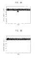
- a stepping distance is set as about 52.474178 mm, about 52.444178 mm, about 52.414178 mm and about 52.394178 mm, and an accumulated exposure light amount can be measured at an overlapped area to show the result on FIG. 8A , FIG. 8B , FIG. 8C and FIG. 8D .
- the x-axis may represent a plurality of areas of the overlapped area, and the y-axis may represent an accumulated exposure light amount at each of the areas.
- a standard unit of the x-axis is ‘ ⁇ m,’ and a standard unit of the y-axis is ‘mJ/cm 2 ’.
- FIG. 8A , FIG. 8B , FIG. 8C and FIG. 8D are graphs illustrating a uniformity of accumulated exposure light amount that is calculated in accordance with exemplary embodiments of the present invention.
- FIG. 8A shows a relationship between areas and an exposure energy if a stepping distance is about 52.474178 mm
- FIG. 8B shows a relationship between areas and an exposure energy if a stepping distance is about 52.444178 mm
- FIG. 8C shows a relationship between areas and an exposure energy if a stepping distance is about 52.414178 mm
- FIG. 8D shows a relationship between areas and an exposure energy when a stepping distance is about 52.394178 mm.
- an area in which an overlapped area is about 170 ⁇ m if the stepping distance is about 52.474178 mm so that it is recognized that an extremely high accumulated exposure light amount is included.
- an area in which an overlapped area is about 200 ⁇ m if the stepping distance is about 52.444178 mm so that it is recognized that a wholly uniformed accumulated exposure light amount is included.
- an area in which an overlapped area is about 230 ⁇ m if the stepping distance is about 52.414178 mm so that it is recognized that an extremely low accumulated exposure light amount is included.
- FIG. 8A , FIG. 8B , FIG. 8C and FIG. 8D if a deviation of the overlapped area is about ⁇ 5%, it is recognized that the overlapped area may be about 190 ⁇ m to about 210 ⁇ m.
- signal wirings having a width of about 0.35 ⁇ m may be formed on a substrate of a large size by overlap distances of about 170 ⁇ m, about 200 ⁇ m, about 230 ⁇ m and about 250 ⁇ m, respectively, based on the result of simulation of light amounts. If the overlap distance is about 170 ⁇ m, portions of the signal wirings may be formed to have a width wider than about 0.35 ⁇ m. When the overlap distance is about 230 ⁇ m to about 250 ⁇ m, portions of the signal wirings may be formed to have a width narrower than about 0.35 ⁇ m.
- a stepping distance of an optical head may be determined by reflecting information on light spot which may be provided to a substrate by an optical head emitting plural laser beams.
- exposure amounts of an overlapped area in which the optical heads are overlapped with each other to be scanned may be uniform so that a substrate of a large size may be exposed by using the optical head.
- an interval distance between the optical heads may be determined if the substrate is scanned by using an optical assembly including the plurality of optical heads.
- processes for compensating an error using Gaussian distribution and controlling an optical head of an optical lithography may be implemented via software, hardware (e.g., general processor, Digital Signal Processing (DSP) chip, an Application Specific Integrated Circuit (ASIC), Field Programmable Gate Arrays (FPGAs), etc.), firmware, or a combination thereof.
- DSP Digital Signal Processing
- ASIC Application Specific Integrated Circuit
- FPGAs Field Programmable Gate Arrays
- firmware or a combination thereof.
- FIG. 9 illustrates exemplary hardware upon which various embodiments of the invention can be implemented.
- a computing system 900 includes a bus 901 or other communication mechanism for communicating information and a processor 903 coupled to the bus 901 for processing information.
- the computing system 900 also includes main memory 905 , such as a random access memory (RAM) or other dynamic storage device, coupled to the bus 901 for storing information and instructions to be executed by the processor 903 .
- Main memory 905 can also be used for storing temporary variables or other intermediate information during execution of instructions by the processor 903 .
- the computing system 900 may further include a read only memory (ROM) 907 or other static storage device coupled to the bus 901 for storing static information and instructions for the processor 903 .
- ROM read only memory
- a storage device 909 such as a magnetic disk or optical disk, is coupled to the bus 901 for persistently storing information and instructions.
- the computing system 900 may be coupled with the bus 901 to a display 911 , such as a liquid crystal display, or active matrix display, for displaying information to a user.
- a display 911 such as a liquid crystal display, or active matrix display
- An input device 913 such as a keyboard including alphanumeric and other keys, may be coupled to the bus 901 for communicating information and command selections to the processor 903 .
- the input device 913 can include a cursor control, such as a mouse, a trackball, or cursor direction keys, for communicating direction information and command selections to the processor 903 and for controlling cursor movement on the display 911 .
- the processes described herein can be provided by the computing system 900 in response to the processor 903 executing an arrangement of instructions contained in main memory 905 .
- Such instructions can be read into main memory 905 from another computer-readable medium, such as the storage device 909 .
- Execution of the arrangement of instructions contained in main memory 905 causes the processor 903 to perform the process steps described herein.
- processors in a multi-processing arrangement may also be employed to execute the instructions contained in main memory 905 .
- hard-wired circuitry may be used in place of or in combination with software instructions to implement the embodiment of the invention.
- reconfigurable hardware such as Field Programmable Gate Arrays (FPGAs) can be used, in which the functionality and connection topology of its logic gates are customizable at run-time, typically by programming memory look up tables.
- FPGAs Field Programmable Gate Arrays
- the computing system 900 also includes at least one communication interface 915 coupled to bus 901 .
- the communication interface 915 provides a two-way data communication coupling to a network link (not shown).
- the communication interface 915 sends and receives electrical, electromagnetic, or optical signals that carry digital data streams representing various types of information.
- the communication interface 915 can include peripheral interface devices, such as a Universal Serial Bus (USB) interface, a PCMCIA (Personal Computer Memory Card International Association) interface, etc.
- USB Universal Serial Bus
- PCMCIA Personal Computer Memory Card International Association
- the processor 903 may execute the transmitted code while being received and/or store the code in the storage device 909 , or other non-volatile storage for later execution. In this manner, the computing system 900 may obtain application code in the form of a carrier wave.
- Non-volatile media include, for example, optical or magnetic disks, such as the storage device 909 .
- Volatile media include dynamic memory, such as main memory 905 .
- Transmission media include coaxial cables, copper wire and fiber optics, including the wires that comprise the bus 901 . Transmission media can also take the form of acoustic, optical, or electromagnetic waves, such as those generated during radio frequency (RF) and infrared (IR) data communications.
- RF radio frequency
- IR infrared
- Computer-readable media include, for example, a floppy disk, a flexible disk, hard disk, magnetic tape, any other magnetic medium, a CD-ROM, CDRW, DVD, any other optical medium, punch cards, paper tape, optical mark sheets, any other physical medium with patterns of holes or other optically recognizable indicia, a RAM, a PROM, and EPROM, a FLASH-EPROM, any other memory chip or cartridge, a carrier wave, or any other medium from which a computer can read.
- a floppy disk a flexible disk, hard disk, magnetic tape, any other magnetic medium, a CD-ROM, CDRW, DVD, any other optical medium, punch cards, paper tape, optical mark sheets, any other physical medium with patterns of holes or other optically recognizable indicia, a RAM, a PROM, and EPROM, a FLASH-EPROM, any other memory chip or cartridge, a carrier wave, or any other medium from which a computer can read.
- the instructions for carrying out at least part of the invention may initially be borne on a magnetic disk of a remote computer.
- the remote computer loads the instructions into main memory and sends the instructions over a telephone line using a modem.
- a modem of a local system receives the data on the telephone line and uses an infrared transmitter to convert the data to an infrared signal and transmit the infrared signal to a portable computing device, such as a personal digital assistant (PDA) or a laptop.
- PDA personal digital assistant
- An infrared detector on the portable computing device receives the information and instructions borne by the infrared signal and places the data on a bus.
- the bus conveys the data to main memory, from which a processor retrieves and executes the instructions.
- the instructions received by main memory can optionally be stored on storage device either before or after execution by processor.
Landscapes
- Physics & Mathematics (AREA)
- General Physics & Mathematics (AREA)
- Health & Medical Sciences (AREA)
- Life Sciences & Earth Sciences (AREA)
- Atmospheric Sciences (AREA)
- Toxicology (AREA)
- Engineering & Computer Science (AREA)
- Environmental & Geological Engineering (AREA)
- Epidemiology (AREA)
- Public Health (AREA)
- Exposure And Positioning Against Photoresist Photosensitive Materials (AREA)
- Exposure Of Semiconductors, Excluding Electron Or Ion Beam Exposure (AREA)
Abstract
Description
Claims (19)
Applications Claiming Priority (3)
| Application Number | Priority Date | Filing Date | Title |
|---|---|---|---|
| KR2010-0014430 | 2010-02-18 | ||
| KR10-2010-0014430 | 2010-02-18 | ||
| KR1020100014430A KR101680754B1 (en) | 2010-02-18 | 2010-02-18 | Method of determining an overlapped distance of an optical head and digital exposure device using the same |
Publications (2)
| Publication Number | Publication Date |
|---|---|
| US20110199620A1 US20110199620A1 (en) | 2011-08-18 |
| US8625109B2 true US8625109B2 (en) | 2014-01-07 |
Family
ID=44369448
Family Applications (1)
| Application Number | Title | Priority Date | Filing Date |
|---|---|---|---|
| US12/902,745 Active 2032-02-14 US8625109B2 (en) | 2010-02-18 | 2010-10-12 | Method of determining an overlap distance of an optical head and digital exposure device using the method |
Country Status (2)
| Country | Link |
|---|---|
| US (1) | US8625109B2 (en) |
| KR (1) | KR101680754B1 (en) |
Families Citing this family (5)
| Publication number | Priority date | Publication date | Assignee | Title |
|---|---|---|---|---|
| KR102171301B1 (en) * | 2013-07-09 | 2020-10-29 | 삼성디스플레이 주식회사 | Digital exposure device using dmd and control method thereof |
| KR101638342B1 (en) * | 2014-08-29 | 2016-07-12 | 주식회사 리텍 | Maskless Exposuer Apparatus Including Multiple Exposure Engine |
| KR20160046016A (en) | 2014-10-17 | 2016-04-28 | 삼성디스플레이 주식회사 | Maskless exposure device and method for compensating cumulative of illumination using the same |
| US10503076B1 (en) * | 2018-08-29 | 2019-12-10 | Applied Materials, Inc. | Reserving spatial light modulator sections to address field non-uniformities |
| KR102674578B1 (en) * | 2019-08-06 | 2024-06-12 | 삼성디스플레이 주식회사 | Method for measuring critical dimension of photo resist pattern |
Citations (11)
| Publication number | Priority date | Publication date | Assignee | Title |
|---|---|---|---|---|
| JPH10193675A (en) * | 1997-01-08 | 1998-07-28 | Fuji Photo Film Co Ltd | Apparatus for forming image |
| US5985496A (en) * | 1996-04-12 | 1999-11-16 | Nikon Corporatioin | Exposure method and apparatus |
| US20010052966A1 (en) * | 2000-02-02 | 2001-12-20 | Seiji Fujitsuka | Scanning exposure method and system |
| EP1375146A1 (en) * | 2001-02-06 | 2004-01-02 | Olympus Optical Co., Ltd. | Image forming apparatus |
| US6876440B1 (en) * | 2003-09-30 | 2005-04-05 | Asml Holding N.V. | Methods and systems to compensate for a stitching disturbance of a printed pattern in a maskless lithography system utilizing overlap of exposure zones with attenuation of the aerial image in the overlap region |
| US20050157286A1 (en) * | 2004-01-16 | 2005-07-21 | Fuji Photo Film Co., Ltd. | Method and system for detecting sensitivity of photosensitive materials and exposure correcting method |
| US7126672B2 (en) * | 2004-12-27 | 2006-10-24 | Asml Netherlands B.V. | Lithographic apparatus and device manufacturing method |
| US7317510B2 (en) * | 2004-12-27 | 2008-01-08 | Asml Netherlands B.V. | Lithographic apparatus and device manufacturing method |
| US7477403B2 (en) * | 2004-05-27 | 2009-01-13 | Asml Netherlands B.V. | Optical position assessment apparatus and method |
| US7956984B2 (en) * | 1993-06-30 | 2011-06-07 | Nikon Corporation | Exposure apparatus, optical projection apparatus and a method for adjusting the optical projection apparatus |
| US20120105865A1 (en) * | 2009-07-17 | 2012-05-03 | Carl Zeiss Smt Gmbh | Microlithographic projection exposure apparatus and related method |
Family Cites Families (2)
| Publication number | Priority date | Publication date | Assignee | Title |
|---|---|---|---|---|
| JP2006251571A (en) | 2005-03-11 | 2006-09-21 | Fuji Photo Film Co Ltd | Light source unit for alignment, alignment apparatus, exposure apparatus, digital exposure apparatus, alignment method, exposure method, and method for setting condition of illumination device |
| JP2006267239A (en) | 2005-03-22 | 2006-10-05 | Fuji Photo Film Co Ltd | Mounting structure of digital micro-mirror device, and image exposure device |
-
2010
- 2010-02-18 KR KR1020100014430A patent/KR101680754B1/en active Active
- 2010-10-12 US US12/902,745 patent/US8625109B2/en active Active
Patent Citations (11)
| Publication number | Priority date | Publication date | Assignee | Title |
|---|---|---|---|---|
| US7956984B2 (en) * | 1993-06-30 | 2011-06-07 | Nikon Corporation | Exposure apparatus, optical projection apparatus and a method for adjusting the optical projection apparatus |
| US5985496A (en) * | 1996-04-12 | 1999-11-16 | Nikon Corporatioin | Exposure method and apparatus |
| JPH10193675A (en) * | 1997-01-08 | 1998-07-28 | Fuji Photo Film Co Ltd | Apparatus for forming image |
| US20010052966A1 (en) * | 2000-02-02 | 2001-12-20 | Seiji Fujitsuka | Scanning exposure method and system |
| EP1375146A1 (en) * | 2001-02-06 | 2004-01-02 | Olympus Optical Co., Ltd. | Image forming apparatus |
| US6876440B1 (en) * | 2003-09-30 | 2005-04-05 | Asml Holding N.V. | Methods and systems to compensate for a stitching disturbance of a printed pattern in a maskless lithography system utilizing overlap of exposure zones with attenuation of the aerial image in the overlap region |
| US20050157286A1 (en) * | 2004-01-16 | 2005-07-21 | Fuji Photo Film Co., Ltd. | Method and system for detecting sensitivity of photosensitive materials and exposure correcting method |
| US7477403B2 (en) * | 2004-05-27 | 2009-01-13 | Asml Netherlands B.V. | Optical position assessment apparatus and method |
| US7126672B2 (en) * | 2004-12-27 | 2006-10-24 | Asml Netherlands B.V. | Lithographic apparatus and device manufacturing method |
| US7317510B2 (en) * | 2004-12-27 | 2008-01-08 | Asml Netherlands B.V. | Lithographic apparatus and device manufacturing method |
| US20120105865A1 (en) * | 2009-07-17 | 2012-05-03 | Carl Zeiss Smt Gmbh | Microlithographic projection exposure apparatus and related method |
Also Published As
| Publication number | Publication date |
|---|---|
| US20110199620A1 (en) | 2011-08-18 |
| KR20110094807A (en) | 2011-08-24 |
| KR101680754B1 (en) | 2016-12-13 |
Similar Documents
| Publication | Publication Date | Title |
|---|---|---|
| US9013674B2 (en) | Exposure apparatus including the exposure head and control method thereof | |
| US8625109B2 (en) | Method of determining an overlap distance of an optical head and digital exposure device using the method | |
| JP7591088B2 (en) | Keeping a spatial light modulator section in reserve to handle field non-uniformities | |
| CN106255925B (en) | Reduction of hot spots for dense features | |
| US9690210B2 (en) | Lithographic apparatus and device manufacturing method | |
| CN1746769B (en) | Lithographic apparatus, method for generating a mask pattern and device manufacturing method using same | |
| CN1763635A (en) | Lithographic apparatus and device manufacturing method | |
| TWI757542B (en) | Method of determining focus and method of determining aberration | |
| JP6808041B2 (en) | Metrology tools and how to use them | |
| CN112272797B (en) | Offset patterns to reduce line fluctuations | |
| US9921488B2 (en) | Maskless exposure method and a maskless exposure device for performing the exposure method | |
| US11768445B2 (en) | Method and apparatus to register template with spatial light modulator | |
| KR101429406B1 (en) | Exposure apparatus and Exposure method using the same | |
| US11815818B2 (en) | Method to achieve non-crystalline evenly distributed shot pattern for digital lithography | |
| US20240280892A1 (en) | Method for correcting errors in photolithographic masks while avoiding damage to rear-side coatings |
Legal Events
| Date | Code | Title | Description |
|---|---|---|---|
| AS | Assignment |
Owner name: SAMSUNG ELECTRONICS CO., LTD., KOREA, REPUBLIC OF Free format text: ASSIGNMENT OF ASSIGNORS INTEREST;ASSIGNORS:YUN, SANG-HYUN;LEE, HI-KUK;BAE, SANG-WOO;AND OTHERS;SIGNING DATES FROM 20100604 TO 20100609;REEL/FRAME:025656/0170 |
|
| AS | Assignment |
Owner name: SAMSUNG DISPLAY CO., LTD., KOREA, REPUBLIC OF Free format text: CHANGE OF NAME;ASSIGNOR:SAMSUNG ELECTRONICS CO., LTD.;REEL/FRAME:028860/0076 Effective date: 20120403 |
|
| FEPP | Fee payment procedure |
Free format text: PAYOR NUMBER ASSIGNED (ORIGINAL EVENT CODE: ASPN); ENTITY STATUS OF PATENT OWNER: LARGE ENTITY |
|
| STCF | Information on status: patent grant |
Free format text: PATENTED CASE |
|
| FPAY | Fee payment |
Year of fee payment: 4 |
|
| MAFP | Maintenance fee payment |
Free format text: PAYMENT OF MAINTENANCE FEE, 8TH YEAR, LARGE ENTITY (ORIGINAL EVENT CODE: M1552); ENTITY STATUS OF PATENT OWNER: LARGE ENTITY Year of fee payment: 8 |
|
| MAFP | Maintenance fee payment |
Free format text: PAYMENT OF MAINTENANCE FEE, 12TH YEAR, LARGE ENTITY (ORIGINAL EVENT CODE: M1553); ENTITY STATUS OF PATENT OWNER: LARGE ENTITY Year of fee payment: 12 |