US8624331B2 - Non-volatile memory devices, methods of manufacturing and methods of operating the same - Google Patents
Non-volatile memory devices, methods of manufacturing and methods of operating the same Download PDFInfo
- Publication number
- US8624331B2 US8624331B2 US12/659,644 US65964410A US8624331B2 US 8624331 B2 US8624331 B2 US 8624331B2 US 65964410 A US65964410 A US 65964410A US 8624331 B2 US8624331 B2 US 8624331B2
- Authority
- US
- United States
- Prior art keywords
- layers
- volatile memory
- memory device
- layer
- fuse
- Prior art date
- Legal status (The legal status is an assumption and is not a legal conclusion. Google has not performed a legal analysis and makes no representation as to the accuracy of the status listed.)
- Expired - Fee Related, expires
Links
Images


Classifications
-
- H—ELECTRICITY
- H10—SEMICONDUCTOR DEVICES; ELECTRIC SOLID-STATE DEVICES NOT OTHERWISE PROVIDED FOR
- H10N—ELECTRIC SOLID-STATE DEVICES NOT OTHERWISE PROVIDED FOR
- H10N70/00—Solid-state devices having no potential barriers, and specially adapted for rectifying, amplifying, oscillating or switching
- H10N70/20—Multistable switching devices, e.g. memristors
-
- H—ELECTRICITY
- H10—SEMICONDUCTOR DEVICES; ELECTRIC SOLID-STATE DEVICES NOT OTHERWISE PROVIDED FOR
- H10B—ELECTRONIC MEMORY DEVICES
- H10B63/00—Resistance change memory devices, e.g. resistive RAM [ReRAM] devices
- H10B63/80—Arrangements comprising multiple bistable or multi-stable switching components of the same type on a plane parallel to the substrate, e.g. cross-point arrays
- H10B63/84—Arrangements comprising multiple bistable or multi-stable switching components of the same type on a plane parallel to the substrate, e.g. cross-point arrays arranged in a direction perpendicular to the substrate, e.g. 3D cell arrays
- H10B63/845—Arrangements comprising multiple bistable or multi-stable switching components of the same type on a plane parallel to the substrate, e.g. cross-point arrays arranged in a direction perpendicular to the substrate, e.g. 3D cell arrays the switching components being connected to a common vertical conductor
-
- H—ELECTRICITY
- H10—SEMICONDUCTOR DEVICES; ELECTRIC SOLID-STATE DEVICES NOT OTHERWISE PROVIDED FOR
- H10N—ELECTRIC SOLID-STATE DEVICES NOT OTHERWISE PROVIDED FOR
- H10N70/00—Solid-state devices having no potential barriers, and specially adapted for rectifying, amplifying, oscillating or switching
- H10N70/011—Manufacture or treatment of multistable switching devices
- H10N70/061—Shaping switching materials
-
- H—ELECTRICITY
- H10—SEMICONDUCTOR DEVICES; ELECTRIC SOLID-STATE DEVICES NOT OTHERWISE PROVIDED FOR
- H10N—ELECTRIC SOLID-STATE DEVICES NOT OTHERWISE PROVIDED FOR
- H10N70/00—Solid-state devices having no potential barriers, and specially adapted for rectifying, amplifying, oscillating or switching
- H10N70/801—Constructional details of multistable switching devices
- H10N70/821—Device geometry
- H10N70/823—Device geometry adapted for essentially horizontal current flow, e.g. bridge type devices
-
- H—ELECTRICITY
- H10—SEMICONDUCTOR DEVICES; ELECTRIC SOLID-STATE DEVICES NOT OTHERWISE PROVIDED FOR
- H10N—ELECTRIC SOLID-STATE DEVICES NOT OTHERWISE PROVIDED FOR
- H10N70/00—Solid-state devices having no potential barriers, and specially adapted for rectifying, amplifying, oscillating or switching
- H10N70/801—Constructional details of multistable switching devices
- H10N70/881—Switching materials
- H10N70/883—Oxides or nitrides
- H10N70/8833—Binary metal oxides, e.g. TaOx
-
- H—ELECTRICITY
- H10—SEMICONDUCTOR DEVICES; ELECTRIC SOLID-STATE DEVICES NOT OTHERWISE PROVIDED FOR
- H10W—GENERIC PACKAGES, INTERCONNECTIONS, CONNECTORS OR OTHER CONSTRUCTIONAL DETAILS OF DEVICES COVERED BY CLASS H10
- H10W20/00—Interconnections in chips, wafers or substrates
- H10W20/40—Interconnections external to wafers or substrates, e.g. back-end-of-line [BEOL] metallisations or vias connecting to gate electrodes
- H10W20/49—Adaptable interconnections, e.g. fuses or antifuses
- H10W20/491—Antifuses, i.e. interconnections changeable from non-conductive to conductive
Definitions
- Example embodiments of inventive concepts relate to semiconductor devices, for example, non-volatile memory devices capable of storing data according to a conduction-insulation transition property.
- Example embodiments of inventive concepts also relate to methods of manufacturing and methods of operating non-volatile memory devices.
- non-volatile memory device having a multi-layer structure When a non-volatile memory device having a multi-layer structure is used, more memory cells may be stacked in a space having the same size as that occupied by a non-volatile memory device having a single-layer structure. However, manufacturing and operating non-volatile memory devices having multi-layer structures are relatively complicated.
- At least one example embodiment of inventive concepts provides a non-volatile memory device including: at least one horizontal electrode and at least one vertical electrode.
- the at least one horizontal electrode and the at least one vertical electrode are disposed to intersect one another at an intersecting region.
- the non-volatile memory device further includes at least one data layer and at least one anti-fuse layer.
- the at least one data layer is disposed at the intersecting region and has a conduction-insulation transition property.
- the at least one anti-fuse layer is connected in series with the at least one data layer.
- the at least one data layer may include a transition metal oxide.
- the at least one data layer may include a vanadium oxide, an aluminum oxide, a bismuth oxide, a titanium oxide, a niobium oxide, a nickel oxide, a copper oxide, zinc oxide, a tin oxide, a zirconium oxide, a silicon oxide, a hafnium oxide, a cobalt oxide, an iron oxide, or combinations thereof.
- the at least one data layer may include a V 2 O 5 , VO 2 , VO, or combinations thereof.
- the at least one anti-fuse layer may include oxide layers, nitride layers, oxy-nitride layers, or combinations of the layers.
- the at least one data layer may have a threshold voltage V TH that is less than a breakdown voltage V AB of the at least one anti-fuse layer.
- the at least one anti-fuse layer may be interposed at the intersecting region between the at least one data layer and the at least one horizontal electrode.
- the at least one anti-fuse layer may be interposed at the intersecting region between the at least one data layer and the at least one vertical electrode.
- At least one of the data layers and the anti-fuse layers may have a pattern at the intersecting region.
- one or more of the at least one horizontal electrode and the at least one vertical electrode may include one or more trenches at the intersecting region.
- One or more of the at least one data layer and the at least one anti-fuse layer may be disposed in the one or more trenches.
- one or more of the at least one data layer and the at least one anti-fuse layer may be disposed to surround the at least one vertical electrode.
- the at least one horizontal electrode and the at least one vertical electrode may be disposed to cross each other perpendicularly or substantially perpendicularly.
- the at least one horizontal electrode may include a first semiconductor having a first conductive type.
- the at least one vertical electrode may include a second semiconductor having a second conductive type.
- the second conductive type may be different from the first conductive type.
- the at least one horizontal electrode, the at least one vertical electrode, or both may include: polysilicon, tungsten (W), aluminum (Al), copper (Cu), molybdenum (Mo), titanium (Ti), tantalum (Ta), ruthenium (Ru), platinum (Pt), palladium (Pd), nickel (Ni), gold (Au), silver (Ag), beryllium (Be), bismuth (Bi), hafnium (Hf), indium (In), manganese (Mn), molybdenum (Mo), lead (Pb), rhodium (Rh), rhenium (Re), tellium (Te), zinc (Zn), zirconium (Zr), cobalt (Co), iridium (Ir), platinum (Pt), an alloy thereof, an oxide thereof, a nitride thereof, a silicide thereof, or a combination thereof.
- At least one other example embodiment of inventive concepts provides a non-volatile memory device including: a plurality of horizontal electrodes stacked in a plurality of layers; and a plurality of vertical electrodes formed in a plurality of rows disposed to intersect the plurality of horizontal electrodes at intersecting regions.
- the non-volatile memory device further includes: a plurality of data layers and a plurality of anti-fuse layers. Each of the plurality of data layers is disposed at a corresponding intersecting region and has a conduction-insulation transition property.
- the plurality of anti-fuse layers are connected in series with the plurality of data layers.
- the plurality of data layers may extend across the stacked layers of the plurality of horizontal electrodes.
- the plurality of anti-fuse layers may extend across the stacked layers of the plurality of horizontal electrodes.
- Each of the plurality of horizontal electrodes may include a plurality of first horizontal electrodes and a plurality of second horizontal electrodes that are spaced apart from each other.
- At least one other example embodiment of inventive concepts provides a non-volatile memory device including: first and second conductive layers that face each other.
- the non-volatile memory device further includes a plurality of data layers and a plurality of anti-fuse layers.
- Each of the plurality of data layers is interposed between the first and second conductive layers and has a conduction-insulation transition property.
- Each of the plurality of anti-fuse layers is interposed between the first and second conductive layers and connected to the plurality of data layers.
- FIG. 1 is a perspective view of a unit cell of a non-volatile memory device according to an example embodiment of inventive concepts
- FIGS. 2A through 2C are perspective views of unit cells of non-volatile memory devices according to other example embodiments of inventive concepts
- FIG. 3 is a perspective view of a non-volatile memory device according to an example embodiment of inventive concepts
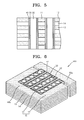
- FIG. 4 is a perspective view of a non-volatile memory device having a stacked-layer structure according to another example embodiment of inventive concepts
- FIG. 5 is a cross-sectional diagram of the non-volatile memory device shown in FIG. 4 taken along the line V-V′;
- FIG. 6 is a perspective view of a non-volatile memory device having a stacked-layer structure according to another example embodiment of inventive concepts
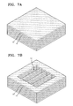
- FIGS. 7A through 7G are perspective views illustrating a method of manufacturing a non-volatile memory device according to an example embodiment of inventive concepts
- FIGS. 8A through 8E are perspective views illustrating a method of manufacturing a non-volatile memory device according to another example embodiment of inventive concepts
- FIG. 9 schematically illustrates a method of operating a non-volatile memory device according to an example embodiment of inventive concepts
- FIG. 10 is a graph showing an example voltage-current characteristic of data layers formed of variable resistive materials and included in the non-volatile memory device according to an example embodiment of inventive concepts
- FIG. 11 is a block diagram of a card according to an example embodiment of inventive concepts.
- FIG. 12 is a block diagram of a system according to an example embodiment of inventive concepts.
- first, second, third, etc. may be used herein to describe various elements, components, regions, layers and/or sections, these elements, components, regions, layers and/or sections should not be limited by these terms. These terms are only used to distinguish one element, component, region, layer or section from another region, layer or section. Thus, a first element, component, region, layer or section discussed below could be termed a second element, component, region, layer or section without departing from the teachings of exemplary embodiments.
- spatially relative terms such as “above,” “upper,” “beneath,” “below,” “lower,” and the like, may be used herein for ease of description to describe one element or feature's relationship to another element(s) or feature(s) as illustrated in the figures. It will be understood that the spatially relative terms are intended to encompass different orientations of the device in use or operation in addition to the orientation depicted in the figures. For example, if the device in the figures is turned over, elements described as “below” or “beneath” other elements or features would then be oriented “above” the other elements or features. Thus, the exemplary term “above” may encompass both an orientation of above and below. The device may be otherwise oriented (rotated 90 degrees or at other orientations) and the spatially relative descriptors used herein interpreted accordingly.
- Example embodiments are described herein with reference to cross-sectional illustrations that are schematic illustrations of example embodiments (and intermediate structures). As such, variations from the shapes of the illustrations as a result, for example, of manufacturing techniques and/or tolerances, are to be expected. Thus, example embodiments should not be construed as limited to the particular shapes of regions illustrated herein but may be to include deviations in shapes that result, for example, from manufacturing. For example, an implanted region illustrated as a rectangle may, typically, have rounded or curved features and/or a gradient of implant concentration at its edges rather than a binary change from implanted to non-implanted region. Likewise, a buried region formed by implantation may result in some implantation in the region between the buried region and the surface through which the implantation takes place. Thus, the regions illustrated in the figures are schematic in nature and their shapes may be not intended to illustrate the actual shape of a region of a device and are not intended to limit the scope of inventive concepts.
- example embodiments are described with reference to the accompanying drawings.
- transformation of forms in the drawings may be expected according to a manufacturing technique and/or tolerance. Accordingly, example embodiments are not limited to the specific forms illustrated in the drawing and may include, for example, changes in the forms which may occur during manufacturing.
- FIG. 1 is a perspective view of a unit cell of a non-volatile memory device according to an example embodiment of inventive concepts.
- a unit cell 1 of a non-volatile memory device includes at least one horizontal electrode 10 , at least one vertical electrode 20 , at least one data layer 30 , and at least one anti-fuse layer 40 .
- the terms ‘horizontal’ and ‘vertical’ are used to distinguish the electrodes 10 and 20 from each other, not to limit the electrodes 10 and 20 .
- the horizontal electrodes 10 and the vertical electrode 20 are disposed to cross each other.
- a vertical electrode 20 is disposed between a pair of horizontal electrodes 10 so as to be perpendicular or substantially perpendicular to (e.g., vertical with respect to) the pair of horizontal electrodes 10 .
- example embodiments are not limited to this arrangement.
- the horizontal electrodes 10 and the vertical electrode 20 may be disposed to cross each other at a given, desired or predetermined angle.
- the horizontal electrodes 10 and the vertical electrode 20 shown in FIG. 1 have the shape of a square pillar; however, example embodiments are not limited thereto. Rather, the horizontal electrodes 10 and the vertical electrode 20 may have various shapes such as a polygonal pillar or a cylindrical pillar.
- the horizontal electrodes 10 and the vertical electrode 20 may be formed of, for example, semiconductor layers such as epitaxial layers or polysilicon layers.
- the horizontal electrodes 10 and the vertical electrode 20 may be formed of a metal layer including tungsten (W), aluminum (Al), copper (Cu), molybdenum (Mo), titanium (Ti), tantalum (Ta), ruthenium (Ru), platinum (Pt), palladium (Pd), nickel (Ni), gold (Au), silver (Ag), beryllium (Be), bismuth (Bi), hafnium (Hf), indium (In), manganese (Mn), molybdenum (Mo), lead (Pb), rhodium (Rh), rhenium (Re), tellium (Te), zinc (Zn), zirconium (Zr), cobalt (Co), iridium (Ir), platinum (Pt) an alloy thereof, an oxide thereof, a nitride thereof, a silicide thereof, combinations thereof or the like
- the at least one data layer 30 is disposed at intersecting regions where the horizontal electrodes 10 and the vertical electrode 20 intersect each other. More specifically, in FIG. 1 , a data layer 30 is disposed to extend along each side wall of the horizontal electrodes 10 that faces the vertical electrode 20 . Alternatively, a data layer 30 may be disposed along each side wall of the vertical electrode 20 at which a horizontal electrode 10 is formed.
- the shape of the data layers 30 illustrated in FIG. 1 are only examples, and the data layer 30 may have other shapes as will be described more fully with reference to FIGS. 2A through 2C .
- the data layers 30 may store data by varying the electrical resistance thereof, and controlling a flow of electrical current between the horizontal electrodes 10 and the vertical electrode 20 .
- the data layers 30 may be conductive or variable resistance materials, which have a resistance that changes according to an applied voltage.
- the data layers 30 may include a metal-insulation transition (MIT) material, which has a resistance that changes according to an applied voltage.
- the data layer 30 may include a transition metal oxide such as a vanadium oxide, an aluminum oxide, a bismuth oxide, a titanium oxide, a niobium oxide, a nickel oxide, a copper oxide, zinc oxide, a tin oxide, a zirconium oxide, a silicon oxide, a hafnium oxide, a cobalt oxide, an iron oxide, combinations thereof or the like.
- the data layer 30 may include V 2 O 5 , VO 2 , VO, or combinations thereof.
- the data layers 30 may include a phase change resistance material having a high-resistance state and a low-resistance state according to a crystalline state of the phase-change resistance material, or a calcogenide compound.
- the above-described materials of the data layers 30 are only examples and example embodiments are not limited thereto.
- the horizontal electrodes 10 may include first semiconductors of a first conductive type
- the vertical electrode 20 may include a second semiconductor of a second conductive type.
- the second conductive type may be different from the first conductive type.
- the first conductive type and the second conductive type may be n-type and p-type, respectively, or vice versa.
- an anti-fuse layer 40 may be optionally disposed at each intersecting region where the horizontal electrodes 10 and the vertical electrode 20 intersect each other.
- an anti-fuse layer 40 is interposed between each horizontal electrode 10 and corresponding data layer 30 .
- the vertical electrode 20 and the data layers 30 are electrically connected to each other.
- each anti-fuse layer 40 is disposed to extend along the side wall of a corresponding one of the horizontal electrodes 10 that faces the vertical electrode 20 .
- the anti-fuse layers 40 may be disposed on the side walls of the vertical electrode 20 .
- the locations of the data layers 30 and the anti-fuse layers 40 are only examples and example embodiments are not limited thereto.
- the locations of the data layers 30 and the anti-fuse layers 40 may be reversed.
- the data layers 30 and the anti-fuse layers 40 may be adjacent to the horizontal electrodes 10 and the vertical electrode 20 , respectively.
- the horizontal electrodes 10 and the data layers 30 may be electrically connected to each other.
- a conductive layer including a conductive material may be interposed between the data layers 30 and the anti-fuse layers 40 .
- the conductive layer may function as an electrode.
- the anti-fuse layers 40 may function as an anti-fuse.
- each of the anti-fuse layers 40 may include an insulating material of which insulating property is lost in response to an applied voltage.
- the non-volatile memory device may be used as a one-time programmable (OTP) memory because the insulating property of the anti-fuse layers 40 material is not recovered.
- OTP memory may be used in products requiring relatively significant memory capacity.
- the anti-fuse layers 40 may include an oxide, a nitride, an oxy-nitride, or combinations thereof.
- the anti-fuse layers 40 may include a silicon oxide, a silicon nitride, a silicon oxy-nitride, or combinations thereof. Also, the anti-fuse layers 40 may include a transition metal oxide, such as, an aluminum oxide, a tantalum oxide, a hafnium oxide, a lanthanum oxide, a bismuth oxide, a titanium oxide, a niobium oxide, a nickel oxide, a copper oxide, a zinc oxide, a tin oxide, a zirconium oxide, a cobalt oxide, an iron oxide, or combinations thereof.
- a transition metal oxide such as, an aluminum oxide, a tantalum oxide, a hafnium oxide, a lanthanum oxide, a bismuth oxide, a titanium oxide, a niobium oxide, a nickel oxide, a copper oxide, a zinc oxide, a tin oxide, a zirconium oxide, a cobalt oxide, an iron oxide, or combinations thereof.
- the anti-fuse layers 40 may be single layers including any one of the materials described above, multi-layer structures including a plurality of stacked single layers, or more complex layer structures including at least two of the above-described materials.
- the materials for forming the anti-fuse layers 40 are only examples and example embodiments are not limited thereto.
- FIGS. 2A through 2C are perspective views of unit cells of non-volatile memory devices according to other example embodiments of inventive concepts.
- the unit cells 1 a , 1 b , and 1 c shown in FIGS. 2A through 2C are similar to the unit cell 1 illustrated in FIG. 1 , and thus, some details thereof will not be repeated.
- the unit cell 1 a may include one or more patterned data layers 30 a and one or more patterned anti-fuse layers 40 a.
- the unit cell 1 a includes a patterned data layer 30 a and a patterned anti-fuse layer 40 a disposed at intersecting regions where horizontal electrodes 10 a and vertical electrode 20 a intersect each other.
- the width of the patterned data layer 30 a and the patterned anti-fuse layer 40 a are the same or substantially the same as the width of the vertical electrode 20 a.
- one or more of the horizontal electrodes 10 b and the vertical electrode 20 b included in the unit cell 1 b may include trenches T.
- one or more of data layers 30 b and anti-fuse layers 40 b may be disposed in the trenches T.
- a trench is formed in each horizontal electrode 10 b , and a data layer 30 b and an anti-fuse layer 40 b are disposed in each trench T.
- the vertical electrode 20 b may include the trenches T and one or more of data layers 30 b and anti-fuse layers 40 b may be disposed in the trenches T.
- both the horizontal electrodes 10 b and the vertical electrode 20 b may include trenches T.
- one of data layers 30 b and anti-fuse layers 40 b may be disposed in the trenches T of the horizontal electrodes 10 b
- the other of the data layers 30 b and anti-fuse layers 40 b may be disposed in the trenches T of the vertical electrode 20 b .
- the horizontal electrodes 10 b and the vertical electrode 20 b are electrically insulated from each other.
- the unit cell 1 c may include a data layer 30 c and an anti-fuse layer 40 c surrounding the vertical electrode 20 c .
- the data layer 30 c and the anti-fuse layer 40 c may be disposed to surround each horizontal electrode 10 c.
- a data layer 30 c and an anti-fuse layer 40 c surround the vertical electrode 20 c.
- the elements included in the unit cells 1 , 1 a , 1 b , and 1 c described with reference to FIGS. 1 through 2C are only examples and inventive concepts are not limited thereto. Characteristics of the elements may be combined.
- FIG. 3 is a perspective view of a non-volatile memory device according to an example embodiment of inventive concepts.
- the non-volatile memory device 100 includes a plurality of the unit cells 1 arranged two-dimensionally.
- example embodiments are not limited thereto and the unit cells 1 a , 1 b , and 1 c of FIGS. 2A through 2C or combinations thereof may be included in the non-volatile memory device 100 .
- the non-volatile memory device 100 includes a plurality of the horizontal electrodes 10 , a plurality of the vertical electrodes 20 , a plurality of data layers 30 , and a plurality of anti-fuse layers 40 .
- the horizontal electrodes 10 and the vertical electrodes 20 are disposed to cross each other.
- the vertical electrodes 20 are disposed between pairs of horizontal electrodes 10 so as to be vertical relative to the horizontal electrodes 10 or to cross each other by a given, desired or predetermined angle.
- the vertical electrodes 20 may be appropriately selected according to the number and length of the horizontal electrodes 10 .
- the numbers of the horizontal electrodes 10 and the vertical electrodes 20 illustrated in FIG. 3 are only examples and example embodiments are not limited thereto.
- the horizontal electrodes 10 and the vertical electrodes 20 are formed as a square pillar; however, example embodiments are not limited thereto.
- the data layers 30 are disposed at intersecting regions where the horizontal electrodes 10 and the vertical electrodes 20 intersect each other.
- data layers 30 are disposed to extend along the side walls of each horizontal electrode 10 .
- the illustrated data layers 30 are only examples and may have various forms as described with reference to FIGS. 1 through 2C .
- Anti-fuse layers 40 may be optionally interposed between the horizontal electrodes 10 and each corresponding data layer 30 .
- the anti-fuse layers 40 are also disposed to extend along the side walls of the horizontal electrodes 10 .
- the illustrated anti-fuse layers 40 are only examples and may have various forms as described with reference to FIGS. 1 through 2C . Also, as described above, the locations of the data layers 30 and the anti-fuse layers 40 may be reversed.
- the non-volatile memory device 100 includes a plurality of memory cells.
- the horizontal electrodes 10 function as word lines and the vertical electrodes 20 function as bit lines.
- the horizontal electrodes 10 may function as bit lines and the vertical electrodes 20 may function as word lines.
- an example configuration and operation of the non-volatile memory device 100 in which the horizontal electrodes 10 function as word lines, is described in more detail.
- the horizontal electrodes 10 include first horizontal electrodes 11 and second horizontal electrodes 12 that are spaced apart from each other.
- the first horizontal electrodes 11 are electrically connected to a first word line 50 a
- the second horizontal electrodes 12 are electrically connected to a second word line 50 b .
- the first word line 50 a and the second word line 50 b are disposed at opposite sides of the first horizontal electrodes 11 and the second horizontal electrodes 12 .
- the first word line 50 a is connected to first ends of the first horizontal electrodes 11
- the second word line 50 b is connected to second ends of the second horizontal electrodes 12 .
- one of the first horizontal electrode 11 and the second horizontal electrode 12 , the vertical electrode 20 , and the data layer 30 disposed there between may form a memory cell as described above with reference to FIGS. 1 through 2C .
- the first horizontal electrodes 11 and the second horizontal electrodes 12 may be accessed through the first word line 50 a and the second word line 50 b , respectively. Accordingly, access to a memory cell may be achieved by selecting one of the first word line 50 a and the second word line 50 b , and the vertical electrode 20 .
- a memory cell of the nonvolatile memory device 100 is programmed by applying a program voltage to the first word line 50 a or the second word line 50 b , and to the vertical electrode 20 .
- the program voltage is greater than a threshold voltage of the anti-fuse layers 40 and the insulating properties of the anti-fuse layers 40 are lost locally.
- a concentration of electrical current causes the insulating properties of the anti-fuse layers 40 to be lost locally in the anti-fuse layers 40 . Accordingly, the data layers 30 adjacent to the broken anti-fuse layers 40 are conductive, and thus, may be programmed.
- a memory cell is read by applying a reading voltage to the first word line 50 a or the second word line 50 b , and the vertical electrode 20 .
- the reading voltage is less than the program voltage and the threshold voltage of the anti-fuse layers 40 , but greater than a threshold voltage of the data layers 30 . Accordingly, an electrical current flows between the horizontal electrodes 10 and the vertical electrode 20 through the data layers 30 adjacent to the anti-fuse layers 40 of which insulating properties are lost due to the program voltage, and thus, a memory cell is read.
- FIG. 4 is a perspective view of a non-volatile memory device 200 having a stacked-layer structure according to another example embodiment of inventive concepts.
- FIG. 5 is a cross-sectional diagram taken along line V-V′ in FIG. 4 .
- the non-volatile memory device 200 includes the unit cells 1 illustrated in FIG. 1 and is similar to the non-volatile memory device 100 of FIG. 3 . Thus, some details thereof will not be repeated. But, the non-volatile memory device 200 including the unit cell 1 of FIG. 1 is only an example, and example embodiments are not limited thereto.
- the non-volatile memory device 200 may include any of the unit cells 1 a , 1 b , and 1 c of FIGS. 2A through 2C .
- the non-volatile memory device 200 includes a plurality of the horizontal electrodes 10 , a plurality of the vertical electrodes 20 , and a plurality of data layers 30 .
- the plurality of horizontal electrodes 10 are formed of a plurality of stacked layers.
- the plurality of the vertical electrodes 20 are formed in a plurality of rows so as to intersect with the plurality of horizontal electrodes 10 at intersecting regions.
- the plurality of data layers 30 are disposed at the intersecting regions where the plurality of the horizontal electrodes 10 and the plurality of the vertical electrodes 20 intersect each other.
- the non-volatile memory device 200 may optionally include an anti-fuse layer 40 interposed between each of the plurality of horizontal electrodes 10 and a corresponding data layer 30 .
- the example embodiment shown in FIGS. 4 and 5 includes the optional anti-fuse layers 40 .
- an anti-fuse layer 40 may be interposed between each of the plurality of vertical electrodes 20 and a corresponding data layer 30 .
- the non-volatile memory device 200 is formed of a plurality of the non-volatile memory devices 100 of FIG. 3 , which are stacked in a plurality of layers. More specifically, the non-volatile memory device 200 includes first conductive layers 13 and insulating layers 14 that are stacked alternately on one another. Accordingly, the plurality of the horizontal electrodes 10 (e.g., the first horizontal electrodes 11 and the second horizontal electrodes 12 ) may be formed of the first conductive layers 13 and the insulating layers 14 interposed between the first conductive layers 13 , thereby forming a plurality of stacked layers.
- the plurality of the horizontal electrodes 10 e.g., the first horizontal electrodes 11 and the second horizontal electrodes 12
- the plurality of the horizontal electrodes 10 may be formed of the first conductive layers 13 and the insulating layers 14 interposed between the first conductive layers 13 , thereby forming a plurality of stacked layers.
- first word lines 50 a and the second word lines 50 b may be formed of the first conductive layers 13 and the insulating layers 14 interposed between the first conductive layers 13 , thereby forming a plurality of stacked layers.
- the first horizontal electrodes 11 and the second horizontal electrodes 12 in each layer may be separated from one another in the same or substantially the same manner as described above with regard to FIG. 3 .
- the first word lines 50 a and the second word lines 50 b in each layer may also be separated from one another in the same or substantially the same manner as described above with regard to FIG. 3 .
- the vertical electrodes 20 extend across the stacked layers of the first horizontal electrodes 11 and the second horizontal electrodes 12 .
- the vertical electrodes 20 are shared by the stack of the first horizontal electrodes 11 and the second horizontal electrodes 12 disposed in each different layer.
- the data layers 30 extend across the stacked layers of the first horizontal electrodes 11 and the second horizontal electrodes 12 . Further, as shown in FIG. 4 , the data layers 30 further extend onto sidewalls of the first word lines 50 a and the second word lines 50 b .
- the data layers 30 are in the form of a square tube surrounding the outer walls of the vertical electrodes 20 in each row. As described above with reference to FIGS. 1 through 2C , the data layers 30 may have various forms.
- the anti-fuse layers 40 extend across the stacked layers of the first horizontal electrodes 11 and the second horizontal electrodes 12 .
- the anti-fuse layers 40 further extend onto the sidewalls of the first word lines 50 a and the second word lines 50 b .
- the anti-fuse layers 40 surround the data layers 30 , thereby having the form of a square tube surrounding the outer walls of the vertical electrodes 20 and/or the data layers 30 disposed in each row.
- the anti-fuse layers 40 may have various forms. Also, the locations of the data layers 30 and the anti-fuse layers 40 may be reversed.
- Example operation of the non-volatile memory device 200 according to at least this example embodiment may be inferred from the operation of the non-volatile memory device 100 of FIG. 3 .
- the capacity of the non-volatile memory device 200 according to at least this example embodiment may be increased relatively easily by increasing the number of the memory cells, for example, the number of first horizontal electrodes 11 and second horizontal electrodes 12 or the number of stacked layers. Accordingly, the non-volatile memory device 200 according to example embodiments may have relatively high integration in the same or substantially the same plane, and thus, may be more suitable as a relatively high-capacity and/or relatively highly integrated product.
- FIG. 6 is a perspective view of a non-volatile memory device having a stacked-layer structure according to another example embodiment of inventive concepts.
- the non-volatile memory device 300 shown in FIG. 6 is similar to the non-volatile memory device 200 of FIG. 4 , and thus, some details thereof will not be repeated.
- vertical electrodes 22 have a cylindrical form and data layers 32 are disposed to surround the vertical electrodes 22 . Accordingly, the data layers 32 fill gaps between the first horizontal electrodes 11 and the second horizontal electrodes 12 , and the vertical electrodes 22 are recessed into the data layers 32 . Also, as described above, anti-fuse layers 42 are formed between the data layers 32 and the first horizontal electrodes 11 , and between the data layers 32 and the second horizontal electrodes 12 . The locations of the data layers 32 and the anti-fuse layers 42 may be reversed.
- FIGS. 7A through 7G are perspective views illustrating a method of manufacturing a non-volatile memory device according to an example embodiment of inventive concepts.
- the first conductive layers 13 may be formed of, for example, semiconductor layers such as epitaxial layers or polysilicon layers, or a metal.
- Example metals include tungsten (W), aluminum (Al), copper (Cu), molybdenum (Mo), titanium (Ti), tantalum (Ta), ruthenium (Ru), platinum (Pt), palladium (Pd), nickel (Ni), gold (Au), silver (Ag), beryllium (Be), bismuth (Bi), hafnium (Hf), indium (In), manganese (Mn), molybdenum (Mo), lead (Pb), rhodium (Rh), rhenium (Re), tellium (Te), zinc (Zn), zirconium (Zr), cobalt (Co), iridium (Ir), an alloy thereof, an oxide thereof, a nitride thereof, a silicide thereof, or combinations thereof.
- the first conductive layers 13 may be doped with first conductive type impurities, for example, n-type impurities or p-type impurities.
- a plurality of trenches 15 are formed in the first conductive layers 13 and the insulating layers 14 .
- the trenches 15 may be formed using a photolithography process and/or an etching process. Portions of the first conductive layers 13 disposed in a plurality of rows along the sidewalls of the trenches 15 are identified as the first and second horizontal electrodes 11 and 12 in FIG. 7F . Moreover, portions of the first conductive layers 13 disposed along the ends of the trenches 15 are identified as the first and second word lines 50 a and 50 b in FIG. 7F . Therefore, an appropriate number of the trenches 15 are formed according to the widths and number of the first and second horizontal electrodes 11 and 12 and first and second word lines 50 a and 50 b.
- each anti-fuse layer 40 is formed in each trench 15 .
- each anti-fuse layer 40 is formed to extend across the inner sidewalls of the first conductive layers 13 and has a given, desired or predetermined thickness so as to partially (e.g., not to completely) fill the trenches 15 .
- the anti-fuse layers 40 may be oxide layers, nitride layers, oxy-nitride layers, or combinations of the layers and may include a material for forming an anti-fuse.
- a data layer 30 is formed on each anti-fuse layer 40 in each trench 15 .
- the data layers 30 extend across the inner sidewalls of the first conductive layers 13 and have a given, desired or predetermined thickness to partially fill (e.g., not completely fill) the trenches 15 .
- second conductive layers 16 are formed on the data layers 30 to fill the trenches 15 .
- the second conductive layers 16 form the vertical electrodes 20 as shown in FIG. 7E .
- the second conductive layers 16 may be formed of semiconductor layers such as epitaxial layers or polysilicon layers, or a metal, as described with respect to the first conductive layers 13 .
- the second conductive layers 16 may be formed of the same as, substantially the same as, or a different material from the first conductive layers 13 .
- the second conductive layers 16 may be doped with second conductive type impurities, which are opposite to the first conductive type impurities of the first conductive layers 13 .
- the second conductive layers 16 may be formed by forming a semiconductor layer or a metal layer using chemical vapor deposition and planarizing the semiconductor layer or the metal layer. The planarization may be performed using an etchback process or chemical-mechanical polishing (CMP).
- CMP chemical-mechanical polishing
- the second conductive layers 16 are patterned to form a plurality of the vertical electrodes 20 .
- the patterning may be performed using a photolithography process and/or an etching process.
- the plurality of the vertical electrodes 20 may be patterned to be electrically separated or insulated from each other.
- each of the first conductive layers 13 are appropriately separated to define the first and second horizontal electrodes 11 and 12 and the first and second word lines 50 a and 50 b .
- the first word line 50 a is connected to the first horizontal electrodes 11 , but separated from the second horizontal electrodes 12 .
- the second word line 50 b is connected to the second horizontal electrodes 12 , but separated from the first horizontal electrodes 11 .
- the structure of FIG. 7F may be formed by cutting between the first horizontal electrodes 11 and the second word line 50 b , and between the second horizontal electrodes 12 and the first word line 50 a in the structure of FIG. 7E . The cutting may be performed using a photolithography process and/or an etching process.
- the first conductive layers 13 and the insulating layers 14 are patterned to have a stepped structure.
- the first conductive layers 13 are exposed.
- the patterning may be performed several times using a photolithography process and/or an etching process.
- the order of forming the stepped structure is only an example and example embodiments are not limited thereto.
- forming of the stepped structure may be performed before, after or directly after forming the plurality of trenches 15 in the first conductive layers 13 and the insulating layers 14 as illustrated in FIG. 7B .
- Contacts 60 which are electrically connected to the first conductive layers 13 exposed in each step of the stepped structure, are formed on the exposed parts of the first conductive layers 13 .
- the first and second word lines 50 a and 50 b and the first and second horizontal electrodes 11 and 12 are electrically connected to the outside (e.g., an external device or apparatus) by the contacts 60 .
- FIGS. 8A through 8E are perspective views illustrating a method of manufacturing the non-volatile memory device according to another example embodiment of inventive concepts.
- the manufacturing method according to at least this example embodiment is a similar to the manufacturing method illustrated in FIGS. 7A through 7G , and thus, some descriptions will not be repeated here.
- a manufacturing operation illustrated in FIG. 8A may follow the manufacturing operations illustrated in FIGS. 7A and 7B .
- anti-fuse layers 42 are formed in the trenches 15 .
- Each anti-fuse layer 42 extends across the inner sidewalls of the first conductive layers 13 and has a given, desired or predetermined thickness to partially fill (e.g., not completely fill) the trenches 15 .
- Data layers 32 are formed on the anti-fuse layers 42 so as to completely fill the trenches 15 .
- the data layers 32 may be formed using, for example, a chemical vapour deposition method and a planarization process. The planarization process may be performed by using an etchback process or CMP.
- the data layers 32 are patterned to form a plurality of holes 35 in the data layers 32 .
- the holes 35 may be formed using a photolithography process and/or an etching process.
- the holes 35 have a circular or substantially circular form.
- example embodiments are not limited thereto and the holes 35 may have a polygonal or elliptical form.
- the vertical electrodes 22 are formed on the data layers 32 .
- the vertical electrodes 22 may be formed by filling conductive materials in the holes 35 and planarizing the holes 35 using chemical vapour deposition.
- the vertical electrodes 22 may include second conductive type impurities.
- each of the first conductive layers 13 are appropriately separated to define the first and second horizontal electrodes 11 and 12 and the first and second word lines 50 a and 50 b .
- the first word line 50 a is connected to the first horizontal electrodes 11 , but separated from the second horizontal electrodes 12 .
- the second word line 50 b is connected to the second horizontal electrodes 12 , but separated from the first horizontal electrodes 11 .
- the first conductive layers 13 and the insulating layers 14 are patterned to have a stepped structure.
- the first conductive layers 13 are exposed.
- the patterning may be performed several times using a photolithography process and/or an etching process.
- the contacts 60 which are electrically connected to the first conductive layers 13 exposed in each step of the stepped structure, are formed on the exposed parts of the first conductive layers 13 .
- the first and second word lines 50 a and 50 b and the first and second horizontal electrodes 11 and 12 are electrically connected to the outside (e.g., an external device or apparatus) by the contacts 60 .
- memory cells having a stacked-layer structure may be formed simultaneously or concurrently. Therefore, manufacturing costs may be reduced by simplifying manufacturing operations.
- the data layers 30 included in the non-volatile memory device are formed of variable resistance materials.
- the data layers 30 and the anti-fuse layers 40 included in the non-volatile memory device according to this example embodiment are connected to each other in series.
- a voltage V D applied to the data layers 30 and a voltage V A applied to the anti-fuse layers 40 are represented by Equation 1 shown below.
- R D and R A are resistances of the data layers 30 and the anti-fuse layers 40 , respectively, and V is an applied external voltage.
- Equation 2 the relationship between a breakdown voltage V AB and a program voltage V p of the anti-fuse layers 40 , the relationship between a threshold voltage V TH and a program voltage V p of the data layer 30 , and the relationship between the breakdown voltage V AB and the threshold voltage V TH of the data layer 30 are represented by Equation 2 shown below.
- V TH ⁇ V AB Equation 2
- Equation 3 the relationship between the threshold voltage V TH and a reading voltage V R of the data layer 30 is represented by Equation 3 shown below.
- the lower limit V R /2 and the upper limit V R of the threshold voltage V TH of the data layer 30 are in a 3-level reading operation.
- inventive concepts are not limited thereto.
- the lower limit and the upper limit of the threshold voltage V TH of the data layer 30 may be changed to V R /3 and 2V R /3, respectively, or 2V R /3 and V R , respectively.
- Thicknesses, types of material, contact areas, or forms of the data layer 30 and the anti-fuse layers 40 may be selected to satisfy the equations above.
- FIG. 9 is a view schematically illustrating an example operation of a non-volatile memory device according to an example embodiment of inventive concepts.
- the unit cells described above are disposed in regions where word lines W/L and bit lines B/L intersect each other.
- a part of the unit cells may be programmed, for example, by applying a program voltage to the unit cells.
- insulating properties of the anti-fuse layers are lost in response to the program voltage.
- the program voltage V P is greater than the breakdown voltage V AB of the anti-fuse layers.
- a first unit cell X, a second unit cell Y, and a third unit cell Z are programmed, whereas the other unit cells are not programmed.
- a reading voltage V is then applied to read the first unit cell X.
- a 3-level reading operation in which half of the reading voltage V is applied to non-read unit cells, is illustrated.
- inventive concepts are not limited thereto.
- the reading voltage V is applied to the word line W/L and the bit line B/L, which pass by the first unit cell X.
- voltages with magnitudes of “V” and “0” may be applied to the word line W/L and the bit line B/L, respectively, which pass by the first unit cell X.
- half of the reading voltage V e.g., a voltage with a magnitude of “V/2” is applied to the word lines W/L and the bit lines B/L, which do not pass by the first unit cell X.
- magnitudes of voltage “V/2” and “0” are respectively applied to the word lines W/L and the bit lines B/L with respect to the second unit cell Y.
- a voltage of “V/2” is applied to the second unit cell Y.
- voltages with magnitudes of “V” and V/2” are respectively applied to the word lines W/L and the bit lines B/L with respect to the third unit cell Z.
- a voltage of “V/2” is applied to the third unit cell Z.
- a voltage of “V/2” is applied to all word lines W/L and the bit lines B/L with respect to the unit cells that are not programmed.
- a voltage of “0” is applied to the unit cells that are not programmed.
- the insulating properties of the anti-fuse layers 40 are broken down because the first unit cell X, the second unit cell Y, and the third unit cell Z are programmed.
- the data layers 30 have the threshold voltage V TH that is greater than 2/V, the data layers 30 function as conductive layers in the first unit cell X, whereas the data layers 30 function as insulating layers in the second unit cell Y and the third unit cell Z. Accordingly, a memory function is available in the first unit cell X.
- FIG. 10 is a graph showing an example voltage-current characteristic of the data layers formed of variable resistance materials and included in the non-volatile memory device according to example embodiments of inventive concepts.
- variable resistive materials before a voltage applied to the variable resistive materials reaches the threshold voltage V TH , a current is nearly 0 and there is little change of current due to an increase of voltage.
- the variable resistive materials have insulating properties before the threshold voltage V TH is applied.
- a voltage applied to the variable resistive materials reaches the threshold voltage V TH , a current is increased relatively significantly and the variable resistance materials have a conduction-insulation transition property or a metal-insulation transition (MIT) property.
- MIT metal-insulation transition
- Such a current-voltage characteristic is partially shown in transition metal oxides such as vanadium oxide, V 2 O 5 , VO 2 , and/or VO.
- transition metal oxides such as vanadium oxide, V 2 O 5 , VO 2 , and/or VO.
- V TH vanadium oxide
- V TH conduction-insulation transition characteristic
- the variable resistance materials may again have an insulating property.
- a current-voltage characteristic of the variable resistive materials may form a hysteresis loop.
- FIG. 11 is a block diagram of a card according to an example embodiment of inventive concepts.
- a controller 510 and a memory 520 are disposed to send/receive electric signals to/from each other.
- the memory 520 sends data to the controller 510 in response to a command from the controller 510 .
- the memory 520 may include the non-volatile memory device 100 according to an example embodiment of inventive concepts.
- the non-volatile memory devices according to the various example embodiments may be disposed to have a NAND or NOR architecture array corresponding to the logic gate design. Such NAND and NOR arrays are generally known in the art.
- the memory arrays disposed in a plurality of rows and columns may have one or more memory array bank (not shown).
- the memory 520 may include the memory array (not shown) or the memory array bank (not shown), all of which are known in the art.
- the memory card 5000 may further include conventional components or elements such as a conventional row decoder (not shown), a column decoder (not shown), input/output (I/O) buffers (now shown), and/or a control resistance materials (not shown) to drive the memory array bank (not shown), all of which are known in the art.
- the memory card 5000 may be used in memory devices, for example, a memory card such as a memory stick card, a smart media (SM) card, a secure digital (SD) card, a mini SD card, a multi media card (MMC), etc.
- SM smart media
- SD secure digital
- MMC multi media card
- FIG. 12 is a block diagram of a system according to an example embodiment of inventive concepts.
- the system 6000 includes a controller 610 , an input/output device 620 , a memory 630 , and an interface 640 .
- the system 6000 may be a mobile system or a system that transmits and/or receives data.
- the mobile system may be a personal digital assistant (PDA), a portable computer, a web tablet, a wireless phone, a mobile phone, a digital music player, a memory card, etc.
- the controller 610 may execute a software program and control the system 6000 .
- the controller 610 may be a microprocessor, a digital signal processor, a microcontroller, or the like.
- the input/output device 630 may be used to input or output data of the system 6000 .
- the system 6000 is connected to an external apparatus, for example, a personal computer or a network, using the input/output device 620 , to send/receive data to/from the external apparatus.
- the input/output device 620 may be a keypad, a keyboard, a display, etc.
- the memory 630 may store codes and/or data for operating the controller 610 and/or may store data processed by the controller 610 .
- the memory 630 may include a non-volatile memory device according to one or more example embodiments of inventive concepts.
- the interface 640 may be a data transmission path between the system 6000 and an external apparatus.
- the controller 610 , the input/output device 620 , the memory 630 , and the interface 640 communicate with one another via a bus 650 .
- the system 6000 may be used for, or incorporated into, a mobile phone, a MP3 player, a navigation system, a portable multimedia player (PMP), a solid state disk (SSD), a household
Landscapes
- Engineering & Computer Science (AREA)
- Manufacturing & Machinery (AREA)
- Semiconductor Memories (AREA)
- Read Only Memory (AREA)
Abstract
Description
V D =V R D/(R D +R A),
V A =V R A/(R D +R A) [Equation 1]
In Equation 1, RD and RA are resistances of the data layers 30 and the
V AB ≦V P R A /R D +R A),
V TH <V P R D/(R D +R A),
VTH<VAB [Equation 2]
V R/2<V TH <V R [Equation 3]
Claims (20)
Applications Claiming Priority (2)
| Application Number | Priority Date | Filing Date | Title |
|---|---|---|---|
| KR10-2009-0110594 | 2009-11-17 | ||
| KR1020090110594A KR20110054088A (en) | 2009-11-17 | 2009-11-17 | Nonvolatile Memory Devices |
Publications (2)
| Publication Number | Publication Date |
|---|---|
| US20110115049A1 US20110115049A1 (en) | 2011-05-19 |
| US8624331B2 true US8624331B2 (en) | 2014-01-07 |
Family
ID=44010673
Family Applications (1)
| Application Number | Title | Priority Date | Filing Date |
|---|---|---|---|
| US12/659,644 Expired - Fee Related US8624331B2 (en) | 2009-11-17 | 2010-03-16 | Non-volatile memory devices, methods of manufacturing and methods of operating the same |
Country Status (3)
| Country | Link |
|---|---|
| US (1) | US8624331B2 (en) |
| KR (1) | KR20110054088A (en) |
| CN (1) | CN102074650A (en) |
Cited By (1)
| Publication number | Priority date | Publication date | Assignee | Title |
|---|---|---|---|---|
| US12490437B2 (en) | 2021-10-18 | 2025-12-02 | Samsung Electronics Co., Ltd. | Non-volatile memory device and method of manufacturing the same |
Families Citing this family (15)
| Publication number | Priority date | Publication date | Assignee | Title |
|---|---|---|---|---|
| JP5558090B2 (en) * | 2009-12-16 | 2014-07-23 | 株式会社東芝 | Resistance variable memory cell array |
| US9227456B2 (en) | 2010-12-14 | 2016-01-05 | Sandisk 3D Llc | Memories with cylindrical read/write stacks |
| US10333064B2 (en) * | 2011-04-13 | 2019-06-25 | Micron Technology, Inc. | Vertical memory cell for high-density memory |
| US9343672B2 (en) * | 2011-06-07 | 2016-05-17 | Samsung Electronics Co., Ltd. | Nonvolatile memory devices, nonvolatile memory cells and methods of manufacturing nonvolatile memory devices |
| KR101957897B1 (en) * | 2012-04-26 | 2019-03-13 | 에스케이하이닉스 주식회사 | Resistance variable memory device and method for fabricating the same |
| US8923050B2 (en) * | 2012-06-15 | 2014-12-30 | Sandisk 3D Llc | 3D memory with vertical bit lines and staircase word lines and vertical switches and methods thereof |
| US9281029B2 (en) | 2012-06-15 | 2016-03-08 | Sandisk 3D Llc | Non-volatile memory having 3D array architecture with bit line voltage control and methods thereof |
| KR102025290B1 (en) * | 2013-03-12 | 2019-09-26 | 에스케이하이닉스 주식회사 | Semiconductor device and electronic device including the same |
| CN106575703B (en) * | 2014-06-26 | 2019-12-17 | 英特尔公司 | Oxide-Based Three-Terminal Resistive Switching Logic Devices |
| CN105185902B (en) * | 2015-08-17 | 2018-04-10 | 河南科技大学 | A kind of resistor-type memory cell |
| CN105390611B (en) * | 2015-10-16 | 2019-01-18 | 福州大学 | A kind of low-power consumption resistance-variable storing device and preparation method thereof based on double storage medium layers |
| JP2018157020A (en) * | 2017-03-16 | 2018-10-04 | 東芝メモリ株式会社 | Storage device and manufacturing method thereof |
| US12317502B2 (en) * | 2019-09-12 | 2025-05-27 | SanDisk Technologies, Inc. | Three-dimensional memory device containing ferroelectric-assisted memory elements and method of making the same |
| US11309332B2 (en) * | 2019-09-12 | 2022-04-19 | Sandisk Technologies Llc | Three-dimensional memory device containing ferroelectric memory elements encapsulated by transition metal-containing conductive elements and method of making thereof |
| CN115910990B (en) * | 2023-02-23 | 2023-05-23 | 长鑫存储技术有限公司 | Antifuse structure and preparation method thereof |
Citations (7)
| Publication number | Priority date | Publication date | Assignee | Title |
|---|---|---|---|---|
| KR20030014653A (en) | 2001-08-09 | 2003-02-19 | 휴렛-팩커드 컴퍼니(델라웨어주법인) | One-time programmable memory using fuse/anti-fuse and vertically oriented fuse unit memory cells |
| KR20030023556A (en) | 2001-09-14 | 2003-03-19 | 휴렛-팩커드 컴퍼니(델라웨어주법인) | Memory device having dual tunnel junction memory cells |
| US20050128840A1 (en) | 2002-08-02 | 2005-06-16 | Darrell Rinerson | Cross point memory array exhibiting a characteristic hysteresis |
| US20060097343A1 (en) * | 2004-11-08 | 2006-05-11 | Ward Parkinson | Programmable matrix array with phase-change material |
| US20080303013A1 (en) * | 2007-06-11 | 2008-12-11 | Thomas Happ | Integrated circuit including spacer defined electrode |
| US20090272958A1 (en) * | 2008-05-02 | 2009-11-05 | Klaus-Dieter Ufert | Resistive Memory |
| US20100012911A1 (en) * | 2005-08-15 | 2010-01-21 | National Institute Of Advanced Industrial Science And Technology | Switching device |
Family Cites Families (3)
| Publication number | Priority date | Publication date | Assignee | Title |
|---|---|---|---|---|
| US7808810B2 (en) * | 2006-03-31 | 2010-10-05 | Sandisk 3D Llc | Multilevel nonvolatile memory cell comprising a resistivity-switching oxide or nitride and an antifuse |
| KR20090037277A (en) * | 2007-10-10 | 2009-04-15 | 삼성전자주식회사 | Cross point memory array |
| KR20090055874A (en) * | 2007-11-29 | 2009-06-03 | 삼성전자주식회사 | Nonvolatile Memory Device and Manufacturing Method Thereof |
-
2009
- 2009-11-17 KR KR1020090110594A patent/KR20110054088A/en not_active Ceased
-
2010
- 2010-03-16 US US12/659,644 patent/US8624331B2/en not_active Expired - Fee Related
- 2010-10-13 CN CN2010105107026A patent/CN102074650A/en active Pending
Patent Citations (7)
| Publication number | Priority date | Publication date | Assignee | Title |
|---|---|---|---|---|
| KR20030014653A (en) | 2001-08-09 | 2003-02-19 | 휴렛-팩커드 컴퍼니(델라웨어주법인) | One-time programmable memory using fuse/anti-fuse and vertically oriented fuse unit memory cells |
| KR20030023556A (en) | 2001-09-14 | 2003-03-19 | 휴렛-팩커드 컴퍼니(델라웨어주법인) | Memory device having dual tunnel junction memory cells |
| US20050128840A1 (en) | 2002-08-02 | 2005-06-16 | Darrell Rinerson | Cross point memory array exhibiting a characteristic hysteresis |
| US20060097343A1 (en) * | 2004-11-08 | 2006-05-11 | Ward Parkinson | Programmable matrix array with phase-change material |
| US20100012911A1 (en) * | 2005-08-15 | 2010-01-21 | National Institute Of Advanced Industrial Science And Technology | Switching device |
| US20080303013A1 (en) * | 2007-06-11 | 2008-12-11 | Thomas Happ | Integrated circuit including spacer defined electrode |
| US20090272958A1 (en) * | 2008-05-02 | 2009-11-05 | Klaus-Dieter Ufert | Resistive Memory |
Cited By (1)
| Publication number | Priority date | Publication date | Assignee | Title |
|---|---|---|---|---|
| US12490437B2 (en) | 2021-10-18 | 2025-12-02 | Samsung Electronics Co., Ltd. | Non-volatile memory device and method of manufacturing the same |
Also Published As
| Publication number | Publication date |
|---|---|
| CN102074650A (en) | 2011-05-25 |
| US20110115049A1 (en) | 2011-05-19 |
| KR20110054088A (en) | 2011-05-25 |
Similar Documents
| Publication | Publication Date | Title |
|---|---|---|
| US8624331B2 (en) | Non-volatile memory devices, methods of manufacturing and methods of operating the same | |
| US9437658B2 (en) | Fully isolated selector for memory device | |
| US9219098B2 (en) | Electronic device having flash memory array formed in at different level than variable resistance memory cells | |
| US8173987B2 (en) | Integrated circuit 3D phase change memory array and manufacturing method | |
| US9812505B2 (en) | Non-volatile memory device containing oxygen-scavenging material portions and method of making thereof | |
| US8995166B2 (en) | Multi-level memory array having resistive elements for multi-bit data storage | |
| US9373665B2 (en) | Resistance change nonvolatile memory device, semiconductor device, and method of manufacturing resistance change nonvolatile memory device | |
| EP2697839B1 (en) | Vertical memory cell for high-density memory | |
| US9646688B2 (en) | Three dimensional non-volatile storage with connected word lines | |
| US8575590B2 (en) | Nonvolatile semiconductor memory device | |
| JP6230229B2 (en) | Stacked RRAM with integrated transistor selector | |
| US20200194667A1 (en) | Variable resistance semiconductor device having oxidation-resistant electrode | |
| US8319291B2 (en) | Non-volatile memory device with data storage layer | |
| US9443910B1 (en) | Silicided bit line for reversible-resistivity memory | |
| KR101497547B1 (en) | Non-volatile memory device | |
| KR20130132373A (en) | Non-volatile memoryu having 3d array of read/write elements with vertical bit lines and laterally aligned active elements and methods thereof | |
| TWI530953B (en) | 3d memory and decoding technologies | |
| US8116113B2 (en) | Cross-point semiconductor memory device and method of manufacturing the same | |
| US20260040577A1 (en) | Microelectronic devices, and related methods of forming microelectronic devices | |
| US20230180641A1 (en) | Variable resistance memory device |
Legal Events
| Date | Code | Title | Description |
|---|---|---|---|
| AS | Assignment |
Owner name: SAMSUNG ELECTRONICS CO., LTD., KOREA, REPUBLIC OF Free format text: ASSIGNMENT OF ASSIGNORS INTEREST;ASSIGNORS:KIM, DEOK-KEE;CHO, CHOONG-RAE;SIGNING DATES FROM 20100309 TO 20100310;REEL/FRAME:024144/0483 |
|
| FEPP | Fee payment procedure |
Free format text: MAINTENANCE FEE REMINDER MAILED (ORIGINAL EVENT CODE: REM.) |
|
| LAPS | Lapse for failure to pay maintenance fees |
Free format text: PATENT EXPIRED FOR FAILURE TO PAY MAINTENANCE FEES (ORIGINAL EVENT CODE: EXP.) |
|
| STCH | Information on status: patent discontinuation |
Free format text: PATENT EXPIRED DUE TO NONPAYMENT OF MAINTENANCE FEES UNDER 37 CFR 1.362 |
|
| FP | Lapsed due to failure to pay maintenance fee |
Effective date: 20180107 |