US8605062B2 - Display device - Google Patents
Display device Download PDFInfo
- Publication number
- US8605062B2 US8605062B2 US12/073,219 US7321908A US8605062B2 US 8605062 B2 US8605062 B2 US 8605062B2 US 7321908 A US7321908 A US 7321908A US 8605062 B2 US8605062 B2 US 8605062B2
- Authority
- US
- United States
- Prior art keywords
- pixels
- detection
- light
- signal
- display device
- Prior art date
- Legal status (The legal status is an assumption and is not a legal conclusion. Google has not performed a legal analysis and makes no representation as to the accuracy of the status listed.)
- Active, expires
Links
Images


Classifications
-
- G—PHYSICS
- G09—EDUCATION; CRYPTOGRAPHY; DISPLAY; ADVERTISING; SEALS
- G09G—ARRANGEMENTS OR CIRCUITS FOR CONTROL OF INDICATING DEVICES USING STATIC MEANS TO PRESENT VARIABLE INFORMATION
- G09G3/00—Control arrangements or circuits, of interest only in connection with visual indicators other than cathode-ray tubes
- G09G3/20—Control arrangements or circuits, of interest only in connection with visual indicators other than cathode-ray tubes for presentation of an assembly of a number of characters, e.g. a page, by composing the assembly by combination of individual elements arranged in a matrix no fixed position being assigned to or needed to be assigned to the individual characters or partial characters
- G09G3/22—Control arrangements or circuits, of interest only in connection with visual indicators other than cathode-ray tubes for presentation of an assembly of a number of characters, e.g. a page, by composing the assembly by combination of individual elements arranged in a matrix no fixed position being assigned to or needed to be assigned to the individual characters or partial characters using controlled light sources
- G09G3/30—Control arrangements or circuits, of interest only in connection with visual indicators other than cathode-ray tubes for presentation of an assembly of a number of characters, e.g. a page, by composing the assembly by combination of individual elements arranged in a matrix no fixed position being assigned to or needed to be assigned to the individual characters or partial characters using controlled light sources using electroluminescent panels
- G09G3/32—Control arrangements or circuits, of interest only in connection with visual indicators other than cathode-ray tubes for presentation of an assembly of a number of characters, e.g. a page, by composing the assembly by combination of individual elements arranged in a matrix no fixed position being assigned to or needed to be assigned to the individual characters or partial characters using controlled light sources using electroluminescent panels semiconductive, e.g. using light-emitting diodes [LED]
- G09G3/3208—Control arrangements or circuits, of interest only in connection with visual indicators other than cathode-ray tubes for presentation of an assembly of a number of characters, e.g. a page, by composing the assembly by combination of individual elements arranged in a matrix no fixed position being assigned to or needed to be assigned to the individual characters or partial characters using controlled light sources using electroluminescent panels semiconductive, e.g. using light-emitting diodes [LED] organic, e.g. using organic light-emitting diodes [OLED]
- G09G3/3225—Control arrangements or circuits, of interest only in connection with visual indicators other than cathode-ray tubes for presentation of an assembly of a number of characters, e.g. a page, by composing the assembly by combination of individual elements arranged in a matrix no fixed position being assigned to or needed to be assigned to the individual characters or partial characters using controlled light sources using electroluminescent panels semiconductive, e.g. using light-emitting diodes [LED] organic, e.g. using organic light-emitting diodes [OLED] using an active matrix
- G09G3/3233—Control arrangements or circuits, of interest only in connection with visual indicators other than cathode-ray tubes for presentation of an assembly of a number of characters, e.g. a page, by composing the assembly by combination of individual elements arranged in a matrix no fixed position being assigned to or needed to be assigned to the individual characters or partial characters using controlled light sources using electroluminescent panels semiconductive, e.g. using light-emitting diodes [LED] organic, e.g. using organic light-emitting diodes [OLED] using an active matrix with pixel circuitry controlling the current through the light-emitting element
-
- G—PHYSICS
- G09—EDUCATION; CRYPTOGRAPHY; DISPLAY; ADVERTISING; SEALS
- G09G—ARRANGEMENTS OR CIRCUITS FOR CONTROL OF INDICATING DEVICES USING STATIC MEANS TO PRESENT VARIABLE INFORMATION
- G09G2300/00—Aspects of the constitution of display devices
- G09G2300/08—Active matrix structure, i.e. with use of active elements, inclusive of non-linear two terminal elements, in the pixels together with light emitting or modulating elements
- G09G2300/0809—Several active elements per pixel in active matrix panels
- G09G2300/0819—Several active elements per pixel in active matrix panels used for counteracting undesired variations, e.g. feedback or autozeroing
-
- G—PHYSICS
- G09—EDUCATION; CRYPTOGRAPHY; DISPLAY; ADVERTISING; SEALS
- G09G—ARRANGEMENTS OR CIRCUITS FOR CONTROL OF INDICATING DEVICES USING STATIC MEANS TO PRESENT VARIABLE INFORMATION
- G09G2300/00—Aspects of the constitution of display devices
- G09G2300/08—Active matrix structure, i.e. with use of active elements, inclusive of non-linear two terminal elements, in the pixels together with light emitting or modulating elements
- G09G2300/0809—Several active elements per pixel in active matrix panels
- G09G2300/0842—Several active elements per pixel in active matrix panels forming a memory circuit, e.g. a dynamic memory with one capacitor
- G09G2300/0861—Several active elements per pixel in active matrix panels forming a memory circuit, e.g. a dynamic memory with one capacitor with additional control of the display period without amending the charge stored in a pixel memory, e.g. by means of additional select electrodes
-
- G—PHYSICS
- G09—EDUCATION; CRYPTOGRAPHY; DISPLAY; ADVERTISING; SEALS
- G09G—ARRANGEMENTS OR CIRCUITS FOR CONTROL OF INDICATING DEVICES USING STATIC MEANS TO PRESENT VARIABLE INFORMATION
- G09G2310/00—Command of the display device
- G09G2310/02—Addressing, scanning or driving the display screen or processing steps related thereto
- G09G2310/0202—Addressing of scan or signal lines
- G09G2310/0218—Addressing of scan or signal lines with collection of electrodes in groups for n-dimensional addressing
-
- G—PHYSICS
- G09—EDUCATION; CRYPTOGRAPHY; DISPLAY; ADVERTISING; SEALS
- G09G—ARRANGEMENTS OR CIRCUITS FOR CONTROL OF INDICATING DEVICES USING STATIC MEANS TO PRESENT VARIABLE INFORMATION
- G09G2320/00—Control of display operating conditions
- G09G2320/02—Improving the quality of display appearance
- G09G2320/0252—Improving the response speed
-
- G—PHYSICS
- G09—EDUCATION; CRYPTOGRAPHY; DISPLAY; ADVERTISING; SEALS
- G09G—ARRANGEMENTS OR CIRCUITS FOR CONTROL OF INDICATING DEVICES USING STATIC MEANS TO PRESENT VARIABLE INFORMATION
- G09G2320/00—Control of display operating conditions
- G09G2320/02—Improving the quality of display appearance
- G09G2320/0285—Improving the quality of display appearance using tables for spatial correction of display data
-
- G—PHYSICS
- G09—EDUCATION; CRYPTOGRAPHY; DISPLAY; ADVERTISING; SEALS
- G09G—ARRANGEMENTS OR CIRCUITS FOR CONTROL OF INDICATING DEVICES USING STATIC MEANS TO PRESENT VARIABLE INFORMATION
- G09G2320/00—Control of display operating conditions
- G09G2320/02—Improving the quality of display appearance
- G09G2320/029—Improving the quality of display appearance by monitoring one or more pixels in the display panel, e.g. by monitoring a fixed reference pixel
-
- G—PHYSICS
- G09—EDUCATION; CRYPTOGRAPHY; DISPLAY; ADVERTISING; SEALS
- G09G—ARRANGEMENTS OR CIRCUITS FOR CONTROL OF INDICATING DEVICES USING STATIC MEANS TO PRESENT VARIABLE INFORMATION
- G09G2320/00—Control of display operating conditions
- G09G2320/04—Maintaining the quality of display appearance
- G09G2320/043—Preventing or counteracting the effects of ageing
Definitions
- the present invention relates to a display device having a light-emitting element such as an organic EL, and particularly to a technique by which temporal changes in characteristics of light emission of an organic EL element are detected.
- a display device hereinbelow, referred to as an organic EL display device (OLED)
- OLED organic electroluminescence
- FED display device a display device in which electron sources using field emission are arranged in a matrix manner and fluorescent materials arranged at anodes are lit so as to form an image
- the organic EL display device has the following characteristics: (1) a backlight is not necessary because the organic EL display device is of a light-emitting type as compared to a liquid crystal display; (2) a voltage required for light emission is as low as 10V or less, and power consumption can be possibly reduced; (3) a vacuum structure is not necessary, so that the organic EL display device can be suitably made lighter and thinner as compared to the plasma display device and the FED display device; (4) response time is as short as several micro seconds, and the characteristics of a moving picture are excellent, and (5) a view angle is as wide as 170 degrees or more.
- the organic EL display device has the above-described characteristics, one of the problems is that there is a phenomenon that the characteristics of light emission of an organic light emitting diode element (hereinbelow, referred to as an OLED element) are changed along with the operation time.
- the temporal changes in characteristics of the OLED element differ depending on pixels. Accordingly, in order to correctly display an image, it is necessary to detect the changes in characteristics of the OLED element of each pixel and to feed back the result to a signal input from a host.
- the changes in characteristics of the OLED element are present as changes in voltage-current characteristics of the OLED element. Specifically, even when a voltage is applied at the same level, a current to flow is decreased along with the operation time. This phenomenon is shown in FIG. 11 .
- the horizontal axis of FIG. 11 represents a voltage applied to the OLED element, and the vertical axis thereof represents a current flowing into the OLED element.
- the characteristic 1 represents an initial characteristic of the OLED element.
- the characteristic 2 represents a characteristic of the OLED element after a certain period of time passed.
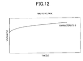
- FIG. 12 shows changes in applied voltage in order to flow a current at the same level into the OLED element.
- the horizontal axis represents an operation time and the vertical axis represents an applied voltage for flowing a constant current into the OLED element.
- FIG. 12 shows that in order to flow a current at the same level to the OLED element, an applied voltage needs to be increased along with the operation time.
- JP-A-2005-156697 and JP-A-2002-341825 describe such techniques.
- the OLED elements of the all pixels are sequentially measured.
- the voltage-current characteristics of the OLED elements of the respective pixels it is necessary to charge floating capacitance due to presence of the floating capacitance in the respective pixels. Accordingly, it takes time to measure each pixel.
- the screen of the display device becomes larger and the definition of the screen becomes higher, it takes a lot of time to measure the all pixels.
- the present invention is to solve the above-described problems, and an object of the present invention is to shorten the measuring time by measuring the voltage-current characteristics of plural OLED elements at a time without sequentially measuring those of the all OLED elements. Concrete means are described as follows.
- a display device in which pixels, each having a light-emitting element that emits a red light, a green light, or a blue light, are formed in a matrix manner, the device including: at least n signal lines for each color; a signal driving circuit which supplies an image signal to the signal lines; a display scanning circuit which supplies a signal for selecting pixels to which the image signal is transmitted; m scanning lines which extend from the display scanning circuit to intersect with the signal lines; a display unit which includes plural pixels coupled to the signal lines and the scanning lines; detection means which measures the characteristics of light emission of the red, green, or blue light-emitting elements of the respective pixels by flowing a constant current from the signal lines to the respective pixels; a detection scanning circuit which supplies, to the scanning lines, a signal for selecting pixels whose characteristics of light emission are measured; and m scanning lines which extend from the detection scanning circuit to intersect with the signal lines, wherein first switches coupled to the signal driving circuit and second switches coupled to the detection means are provided for the signal lines, plural second switches coupled to the detection means are selected
- the display device including a signal driving circuit unit which supplies an image signal, the display scanning circuit, the detection scanning circuit, and a detection unit which detects the characteristics of the light-emitting elements, according to (1), wherein there are provided switch means which control connection between a field effect transistor for driving the light-emitting elements and the detection unit on the basis of the image signal input to the pixels.
- the means (1) since plural light-emitting elements can be measured at a time in order to feed back the characteristics of light emission of the light-emitting elements to the image signal, it is possible to shorten the detection time and to frequently feed back the characteristics, thus realizing a correct tone display.
- the means (2) since the voltage-current characteristics are measured as changes in characteristics of the light-emitting elements, it is possible to easily detect changes in characteristics of light emission.
- the means (3) since plural pixels detected at the same time have the same color, it is possible to change the number of pixels detected at the same time and a current for measuring in accordance with characteristics of the light-emitting elements of each color.
- the means (6) since plural pixels detected at the same time include pixels that emit lights of different colors, it is possible to measure changes in characteristics of the pixels of a combination of three R, G, and B colors at the same time for feedback.
- the means (7) since plural OLED elements can be measured at a time in order to feed back the characteristics of light emission of the OLED elements to the image signal, it is possible to shorten the measuring time and to frequently feed back the characteristics, thus realizing a correct tone display.
- the means (8) in the case of detecting plural light-emitting elements at the same time, the number of light-emitting elements with high light-emitting efficiency detected at the same time is decreased and the number of light-emitting elements with low light-emitting efficiency detected at the same time is increased. Accordingly, a current value to flow per pixel is decreased and the detection voltage is lowered, thus realizing a system with low electric power.
- the means (9) in the case of detecting plural light-emitting elements at the same time, the number of light-emitting elements, detected at the same time, for which a current necessary for detection is large, is increased and the number of light-emitting elements, detected at the same time, for which a current necessary for detection is small is decreased. Accordingly, a current value to flow per pixel is decreased and the detection voltage is lowered, thus realizing a system with low electric power.
- the TFT for controlling the input or output of a current for image formation and the TFT for detecting the characteristics of the OLED elements are provided, a current for image formation and a current for measuring the characteristics of the OLED elements can be allowed to flow into the OLED elements at different timings in one frame.
- FIG. 1 is a circuit configuration of a display device according to a first embodiment
- FIG. 2 is a timing chart showing an operation according to the first embodiment
- FIG. 3 is a circuit configuration of a display device according to a second embodiment
- FIG. 4 is a timing chart showing an operation according to the second embodiment
- FIG. 5 is a circuit configuration of a display device according to a third embodiment
- FIG. 6 is a circuit configuration of a display device according to a fourth embodiment
- FIG. 7 is a circuit configuration of a pixel portion according to a fifth embodiment
- FIG. 8 is a circuit configuration of a display device using the pixel in FIG. 7 ;
- FIG. 9 is a circuit configuration of a pixel portion according to a sixth embodiment.
- FIG. 10 is a circuit configuration of a display device using the pixel in FIG. 9 ;
- FIG. 11 is an example of temporal changes in voltage-current characteristics of OLED elements
- FIG. 12 is an example of temporal changes in voltage between terminals of the OLED elements
- FIGS. 13A and 13B are examples of products in which the present invention is used.
- FIGS. 14A and 14B are other examples of products in which the present invention is used.
- FIG. 1 is a circuit diagram showing a display device of the present invention.
- pixels each having an OLED element that emits a red light, a green right, or a blue light on the basis of an image signal, in a matrix manner.
- PX 1 denotes a pixel that emits a red light
- PX 2 denotes a pixel that emits a green light
- PX 3 denotes a pixel that emits a blue light.
- pixels with the same color are arranged in the vertical direction, and a red pixel (R), a green pixel (G), and a blue pixel (B) are arranged in this order in the horizontal direction.
- n signal lines for each color namely, 3n signal lines in total, in the horizontal direction
- m scanning lines or detection switch controlling lines TSCs in the vertical direction.
- a display scanning circuit 200 On the left side of the screen, there is provided a display scanning circuit 200 . Data writing into each pixel and light emission of each pixel are performed on a scanning-line basis, and the scanning lines extend from the display scanning circuit 200 in the screen direction.
- a detection scanning circuit 150 On the right side of the screen, there is arranged a detection scanning circuit 150 . Detection of the characteristics of each pixel is performed on a scanning-line basis, independently from operations such as data writing into each pixel and light emission of each pixel. A detection operation is performed on a line basis of the screen.
- the detection switch controlling line TSC extends for each line from the detection scanning circuit 150 in the screen direction.
- a signal driving circuit On the upper side of the screen, there is provided a signal driving circuit.
- An image signal is input to the signal driving circuit from a host through a signal input line.
- Image data that is serially transmitted from the host to the signal driving circuit are output to the screen for each line at a time.
- Signal lines through which image data is transmitted to the respective pixels extend from the signal driving circuit in the screen direction.
- the detection system 120 includes a constant current source 112 , a buffer amplifier 114 , an analog-digital converter 115 , and a memory 113 .
- the constant current source 112 is used for measuring the voltage-current characteristics of each OLED element.
- the constant current source 112 supplies a current to each OLED element, and measures the voltage-current characteristic of each OLED element by measuring an anode potential of each OLED element.
- the buffer amplifier amplifies an anode voltage of each OLED element, and outputs the amplified anode voltage to the analog-digital converter 115 .
- the analog-digital converter 115 converts the anode voltage of each OLED element from the buffer amplifier 114 into digital data, and inputs the digital data into the memory 113 .
- the memory 113 stores the voltage-current characteristics of the all OLED elements. The voltage-current characteristics of the OLED elements stored in the memory 113 are fed back to the image data transmitted from the host so as to be supplied to each pixel as an image data signal.
- a detection line 116 that extends from the detection system 120 is arranged in parallel to each signal line.
- a signal line analog switch SSW is arranged for each signal line, and a checking line analog switch is arranged for each checking line. Whether an image signal is supplied to the pixels or the voltage-current characteristics of the OLED elements are measured is determined by these analog switches.
- the checking lines are coupled to the signal lines via the respective analog switches. When the signal line analog switch SSW is turned on, the checking line analog switch is turned off, and image signal data is supplied to the pixels. In addition, when the checking line analog switch is turned on, the signal line analog switch SSW is turned off, and the voltage-current characteristics of the OLED elements can be detected.
- Digital switches are provided between the respective signal lines and the pixels.
- the digital switches are provided for each color.
- An R switch, a G switch, and a B switch are provided for the red pixel, the green pixel, and the blue pixel, respectively.
- the R switch, the G switch, and the B switch are controlled by an R switch controlling line RSCL, a G switch controlling line GSCL, and a B switch controlling line BSCL, respectively.
- the R switch, the G switch, and the B switch are used for detecting the characteristics of the OLED elements for each color at a time, or for a single color.
- Timing of supplying a scanning signal from the display scanning circuit 200 to the pixels, timing of supplying a data signal from the signal driving circuit to the pixels, and supplying of a detection signal from the detection scanning circuit 150 are controlled by a timing controller 110 .
- a period of one frame is divided into a display period and a blanking period in the present invention.
- the display period differs depending on display systems. In one of the systems, the display period is divided into a period during which image data is written into the respective pixels and a period during which the OLED elements are allowed to actually emit lights so as to display an image. In the other of the systems, the OLED elements are allowed to emit lights immediately after image data is written into the pixels.
- the present invention can be implemented in both of the systems.
- the blanking period is a period during which neither writing of image data nor image display is performed.
- changes in characteristics of the OLED elements are detected. Since the blanking period is a period during which neither writing of image data nor image display is performed, it is impossible to set the period longer. Accordingly, it is difficult to detect the characteristics of the all OLED elements during the blanking period in one frame. In this case, the characteristics of the all OLED elements are detected in plural different frames. However, if it takes a long time to detect the characteristics, measuring of the all OLED elements requires the large number of frames, and thus feedback can not be performed in real time. Accordingly, it is necessary to perform the detection of the characteristics of the OLED elements in a short time.
- the measuring of the OLED elements is not performed for each OLED element, but the measuring of the characteristics of plural OLED elements is performed all together so as to shorten the measuring time, thus realizing appropriate feedback of the characteristics of the OLED elements.
- human eyes are unable to recognize the pixels of the display device one by one. Accordingly, if the characteristics of the OLED elements are fed back to an image signal as feedback data obtained by measuring plural OLED elements all together, no problem practically occurs in many cases.
- the present invention is based on such knowledge.
- FIG. 2 is a timing chart showing an operation in the case of detecting the characteristics of the OLED elements in the circuit shown in FIG. 1 .
- the signal line analog switches SSWs are turned off.
- an ON-signal is transmitted to the R switch controlling line RSCL, and the R switch is turned on, so that the characteristics of the R OLED elements can be measured.
- the R pixels on the first line of the screen are selected.
- the checking line analog switches are turned on, two by two at a time.
- the switches are turned on, two by two at a time, such as SWR 1 /SWR 2 and SWR 3 /SWR 4 , as shown in FIG. 2 .
- a time such as SWR 1 /SWR 2 and SWR 3 /SWR 4 , as shown in FIG. 2 .
- an ON-signal is supplied to the detection switch controlling line TSC 2 , and the measuring of the R pixels on the second line is similarly performed. This operation is repeated to the m-th line at the lowermost of the screen, so that the measuring of the all R pixels is completed.
- the measuring of the OLED elements of the all R pixels is finished.
- the measuring of the OLED elements of the G pixels is performed. Specifically, the R switch is turned off, and the G switch is turned on through the G switch controlling line GSCL. Accordingly, the G pixels are selected. Thereafter, the detection switch controlling line TSC 1 is turned on, so that the G pixels on the first line are ready to be selected. In this state, the switches are turned on, two by two at a time, such as SWG 1 /SWG 2 and SWG 3 /SWG 4 , as shown in FIG. 2 .
- the measuring time can be shortened to half that of the conventional technique.
- two pixels that are continuously arranged in the horizontal direction are measured in the description of the first embodiment, two pixels are not necessarily arranged in a continuous manner, but may be arranged in a dispersed manner. That is, the first and third pixels from the left may be measured first, and then the second and fourth pixels may be measured. Further, the number of pixels measured at the same time is not limited to 2, but may be 3 or more.
- the measuring of, for example, two pixels at a time requires an increased capacity of the constant current source 112 .
- the capacity of the constant current source 112 needs to be increased to twice due to floating capacitance common to two pixels. Even in the case of measuring three or more pixels at a time, the same concept can be applied.
- FIG. 3 is a circuit diagram of a display device showing a second embodiment of the present invention.
- a difference between the second embodiment and the first embodiment is that each of the detection switch controlling lines TSCs extending from the detection scanning circuit 150 is mutually coupled to the pixels of two lines.
- the other configuration is the same as FIG. 1 of the first embodiment.
- FIG. 4 is a timing chart showing an operation in the case of detecting the characteristics of the respective OLED elements in the circuit shown in FIG. 3 .
- the signal line analog switches SSWs are turned off, as similar to the first embodiment.
- an ON-signal is transmitted to the R switch controlling line RSCL, and the R switch is turned on, so that the characteristics of the R OLED elements can be measured.
- the R pixels on the first and second lines of the screen are selected.
- the checking line analog switches are sequentially turned on from the left side of the screen, the R pixels on the first and second lines are checked at a time.
- the characteristics of the OLED elements of 2n R pixels on the first and second lines can be measured.
- the measuring of the OLED elements of the G pixels is performed. Specifically, the R switch is turned off, and the G switch is turned on through the G switch controlling line GSCL. Accordingly, the G pixels are selected.
- the measuring of the OLED elements of the G pixels is the same as the detection of the OLED elements of the R pixels.
- the detection of the OLED elements of the B pixels is also the same.
- the measuring time required for the all pixels can be shortened to half that of the conventional technique.
- two pixels that are continuously arranged in the vertical direction are measured in the description of the second embodiment, two pixels are not necessarily arranged in a continuous manner, but may be arranged in a dispersed manner. That is, the pixels on the first and third lines from the above may be measured first, and then the pixels on the second and fourth lines may be measured. Further, the number of pixels measured at the same time is not limited to 2, but may be 3 or more.
- FIG. 5 is a circuit diagram of a display device showing a third embodiment of the present invention.
- a characteristic of the third embodiment shown in FIG. 5 is that the detection system 120 and the group of detection switches are arranged on the lower side opposite to the signal driving circuit.
- the detection system 120 is arranged on the lower right side of the screen.
- the configuration of the detection system 120 is the same as those in the first and second embodiments.
- FIG. 5 is an example in which the R, G, and B pixels are detected for each color on a two-by-two basis at a time.
- a display R switch controlled by a display R switch controlling line DRSCL a display G switch controlled by a display G switch controlling line DGSCL, and a display B switch controlled by a display B switch controlling line DBSCL in FIG. 5 are turned off.
- a detection R switch controlled by a detection R switch controlling line TRSCL, a detection G switch controlled by a detection G switch controlling line TGSCL, and a detection B switch controlled by a detection B switch controlling line TBSCL are turned on.
- an image is displayed in a state where all the detection line analog switches SWs are turned off.
- an arbitrary number of pixels can be detected at a time by bundling the lines together.
- the number of pixels is not limited to 6, but the number of pixels detected at a time may be increased or decreased in accordance with the size of the detection system 120 . Further, it is not necessary to detect the pixels at different timings for each color in the third embodiment, but the pixels of the respective colors can be measured at the same time.
- the detection method in the third embodiment is the same as those in the first and second embodiments.
- the display R switch, the display G switch and the display B switch are turned off, and a detection operation is accordingly ready to be performed.
- the detection switch controlling line TSC 1 By turning on the detection switch controlling line TSC 1 , the detection of the characteristics of the pixels on the first line is performed.
- the detection R switch, the detection G switch, and the detection B switch are turned on, and the detection line analog switch SWR 1 is closed, the characteristics of the OLED elements for six pixels can be detected.
- the kinds or number of colors of the OLED elements to be detected at a time can be arbitrarily selected.
- the detection switch controlling line TSC 2 is selected, and an operation of detecting the pixels on the second line is performed. This operation is repeated to the m-th line, so that the measuring of the all pixels is completed.
- the detection system 120 and the group of detection switches are arranged on the lower side of the screen opposite to the signal driving circuit, plural analog switches can be omitted, and it is possible to increase the degree of freedom of the number of and a combination of pixels to be detected at the same time in the detection operation.
- FIG. 6 is a fourth embodiment of the present invention.
- the detection system 120 and the group of detection switches are arranged on the lower side of the screen opposite to the signal driving circuit, as similar to the third embodiment.
- FIG. 6 largely differs from FIG. 5 is that the number of OLED elements measured at a time differs depending on the colors.
- the OLED elements differ in light-emitting efficiency depending on the colors. Specifically, even if a current is allowed to flow at the same level, the light-emitting intensity differs depending on the colors. For example, in the case where the output voltage of the buffer amplifier 114 is uniformed to a constant voltage when the blue OLED elements are the lowest in light-emitting efficiency, a current value necessary for detecting the characteristics of the blue OLED elements is higher than that necessary for detecting the characteristics of the OLED elements of the other colors. Thus, when the value of the current source is made constant, the number of OLED elements that can be detected at a time differs depending on the colors. If the number of blue OLED elements that can be detected at a time is made smaller than that of the OLED elements of the other colors, a range of the output voltage is uniformed while the size of the constant current source 112 is constant.
- FIG. 6 shows a case in which two each of the red and green OLED elements are detected at a time, and the blue OLED elements are detected one by one. It is assumed in the example of the display device that a current twice as high as that for the red or green OLED elements needs to flow into the blue OLED elements. In this case, the constant current source 112 having a current higher than a constant value is necessary for the blue OLED elements, irrespective of whether the red or green OLED elements are detected on a plural basis at a time. Thus, according to the fourth embodiment, by detecting two each of the red and green OLED elements at a time, the detecting time can be shortened without changing the size of the detection system 120 .
- the combination is not limited to the above, but may be variously changed in the fifth embodiment.
- the red OLED elements are different in light-emitting characteristics from the green OLED elements
- the number of all the red, green, and blue OLED elements detected at a time can be changed. Then, the number of OLED elements detected at a time may be changed in accordance with the light-emitting efficiency of the OLED elements.
- X 1 ⁇ X 2 the light-emitting efficiency of the OLED elements is represented as X 1 and the light-emitting efficiency of OLED elements 2 is represented as X 2
- N 1 ⁇ N 2 the number of OLED elements detected at a time is represented as N 1 and the number of OLED elements 2 detected at a time is represented as N 2
- the detecting speed becomes faster because the detection is performed based on the OLED elements for which a large amount of current is necessary.
- N 1 ⁇ N 2 the amount of current distributed per one pixel is decreased.
- the detecting speed becomes slower than that in the case of N 1 ⁇ N 2 , the OLED elements are detected at a low voltage, thus leading to low electric power of neighboring measuring systems.
- Y 1 ⁇ Y 2 a current for the OLED elements at a certain voltage is represented as Y 1 and a current for the OLED elements 2 is represented as Y 2
- M 2 ⁇ M 1 the number of OLED elements detected at a time is represented as M 1 and the number of OLED elements 2 detected at a time is represented as M 2
- the detection speed is given a priority because the detection is performed based on the OLED elements for which a large amount of detection current per one pixel is necessary. If M 1 ⁇ M 2 is satisfied, the detection voltage is lowered, and thus the lower electric power of the detection systems is given a priority.
- An operation of detecting the respective OLED elements in the fourth embodiment is the same as that in the third embodiment.
- the OLED elements can be detected at a time without increasing the circuit size of the detection system 120 . Accordingly, it is possible to rapidly detect the characteristics of the OLED elements while suppressing the rise of the cost of the display device.
- FIG. 7 is an example of a pixel configuration in which the present invention is implemented.
- an OLED driving TFT 3 a lighting TFT switch 2 , and an OLED element 1 are coupled to each other in series between a power source line 51 and a reference potential.
- the reference potential is a potential that serves as a reference for the display device, and is a wide concept including a ground.
- the lighting TFT switch 2 is a switch for determining whether or not the OLED element 1 is allowed to emit a light.
- the OLED driving TFT 3 is a TFT that controls the tone of light emission of the OLED element 1 in accordance with an image signal.
- the OLED driving TFT 3 is configured by a P-type TFT.
- a carrier of a transistor serves as a hole in the P-type TFT and a carrier of a transistor serves as an electron in an N-type TFT.
- FIG. 7 when a select line is selected, a select switch 6 is turned on, and image signal data from a signal line 54 is input.
- the image signal data is stored in a retentive capacitance 4 .
- the select switch 6 is closed, a charge in accordance with the image signal data is stored in the retentive capacitance 4 , and a gate potential of the OLED driving TFT 3 is retained.
- the lighting switch is turned on in this state, a current flows into the OLED element 1 in accordance with the gate potential of the OLED driving TFT 3 to form an image.
- a detection switch 7 is coupled between the lighting TFT switch 2 and the OLED element 1 , and the detection switch 7 is controlled by the detection switch controlling line TSC 56 extending from the detection scanning circuit 150 .
- the lighting TFT switch 2 is turned off for a certain period of time in one frame, so that light emission of the OLED element 1 for image formation is stopped.
- the detection switch 7 is turned on, and a current from the constant current source 112 of the detection system 120 is allowed to flow into the OLED element 1 , so that the detection of the characteristics of the OLED element 1 is performed.
- FIG. 8 is an example in which the pixel structure shown in FIG. 7 is applied to the display device in FIG. 1 .
- the screen is composed of plural pixels, only four pixels are displayed in FIG. 8 .
- the display scanning circuit 200 is provided on the left side of the screen.
- Select switch lines 55 and lighting switch lines 53 extend from the display scanning circuit 200 to the respective pixels.
- Image signal data can be written for each line of the screen through the select switch lines 55 .
- the lighting switch lines 53 are coupled to gates of the lighting TFT switches 2 of the respective pixels, so as to control whether or not the OLED element 1 is lit on.
- the detection scanning circuit 150 is provided on the right side of the screen.
- the detection switch controlling lines TSCs extend from the detection scanning circuit 150 so as to control the detection switches 7 . When the detection switches 7 are turned on, the voltage-current characteristics of the OLED element 1 can be detected. When the detection switches 7 are turned on, the lighting TFT switches 2 are turned off.
- the signal driving circuit is provided on the upper side of the screen.
- the signal lines 54 extend from the signal driving circuit to the respective pixels.
- the R switches, G switches, or B switches configured by the signal line analog switches SSWs and MOSs are provided for the signal lines 54 .
- the signal lines 54 are coupled to sources of the select switches 6 and sources of the detection switches 7 of the respective pixels.
- the detection system 120 is provided on the right upper side of the screen.
- the detection system 120 is configured as described in FIG. 1 .
- a detection line 116 extends from the detection system 120 , and is branched so as to be coupled to the respective signal lines 54 in parallel.
- the branched detection lines 116 are coupled to the signal lines 54 via the detection line analog switch SWR 1 and the like.
- the signal line analog switch SSW is turned on, an image is displayed.
- the detection line analog switch SWR 1 and the like are turned on, the detection of the characteristics of the respective OLED elements 1 is performed.
- All of the R switches, G switches and the like which are provided for the signal lines 54 and are MOS switches are usually turned on when an image is displayed.
- the MOS switches corresponding to the pixels of the respective colors are turned on, and the other MOS switches are turned off.
- the detection switches 7 are provided for the respective pixels, and the detection switch controlling lines TSCs extending from the detection scanning circuit 150 are coupled to the gates of the detection switches 7 in the fifth embodiment. Accordingly, the detection of the characteristics of the respective OLED elements 1 is controlled by a signal from the detection scanning circuit 150 .
- the pixel shown in FIG. 7 is applied to the display device in FIG. 1 .
- the pixel configuration in FIG. 7 can be applied to not only the display device in FIG. 1 , but also the display devices in FIGS. 3 , 5 , 6 , and the like.
- FIG. 9 is another example of the pixel configuration in which the present invention is implemented.
- the OLED driving TFT 3 controls the tone of the OLED element 1 .
- the tone display is performed in such a manner that the gate potential of the OLED driving TFT 3 is retained by the charge retained by the retentive capacitance 4 .
- the gate potential of the OLED driving TFT 3 is affected by the variations in the threshold voltage VTH and correct tone display can not be performed.
- the pixel circuit in FIG. 9 is configured as countermeasures against the problem.
- the OLED element 1 , the lighting TFT switch 2 , and the OLED driving TFT 3 are coupled to each other in series between the power source line 51 and the reference potential.
- the lighting TFT switch 2 is a switch for determining whether or not the OLED element 1 is allowed to emit a light.
- the OLED driving TFT 3 is a TFT that controls the tone of light emission of the OLED element 1 in accordance with an image signal.
- the OLED driving TFT 3 is configured by an N-type TFT. Accordingly, all the pixel portions can be advantageously manufactured by N-type processes in the sixth embodiment.
- the pixels are used for a display device of a type which is driven by dividing a display period in one frame into a period during which data is written and a period during which an image is actually displayed.
- a reset TFT switch 5 when a reset TFT switch 5 is turned on in a state where the lighting TFT switch 2 is turned off, image signal data is written into the retentive capacitance 4 through the signal line 54 .
- the lighting TFT switch 2 is turned on for a short period of time while the reset TFT switch 5 is turned on after the image data is written, a current flows into the OLED driving TFT 3 .
- This state is regarded as a state in which the OLED element 1 and the OLED driving TFT 3 form an inverter.
- the gate and source of the OLED driving TFT 3 are shorted by the reset TFT switch 5 . Accordingly, the gate potential of the OLED driving TFT 3 is set at a point, on a characteristic curved-line that determines the relation between the gate and the source of the OLED driving TFT 3 , where the source of the OLED driving TFT 3 is equal to the gate thereof in potential.
- the gate potential of the OLED driving TFT 3 in this case is uniquely determined by the threshold voltage VTH of the OLED driving TFT 3 . Since a signal voltage in accordance with the gate potential is written, effects caused due to the variations in the threshold voltage VTH of the OLED driving TFT 3 can be eliminated.
- the reset TFT switch 5 and then the lighting TFT switch 2 are turned off, a charge that correctly reflects the signal voltage is maintained at the retentive capacitance 4 .
- the following driving method is used for an organic EL display device for which the pixel shown in FIG. 9 is used. Specifically, one frame is divided into a period during which a data signal is written and a period during which light is emitted. In the data-writing period, an image signal is written into the all pixels by the above-described manner. Thereafter, a current is allowed to flow into the OLED elements 1 by closing the lighting TFT switches 2 for the all pixels, so that an image is formed. Specifically, the first half of one frame is virtually displayed in black and an image is formed in the last half of one frame.
- the detection switch 7 is coupled between the lighting TFT switch 2 and a cathode of the OLED element 1 , and the detection switch 7 is controlled by the detection switch controlling line TSC extending from the detection scanning circuit 150 .
- the lighting TFT switch 2 is turned off for a certain period of time in one frame, so that light emission of the OLED element 1 for image formation is stopped.
- the detection switch 7 is turned on, and a current from the constant current source 112 of the detection system 120 is allowed to flow into the OLED element 1 , so that the detection of the characteristics of the OLED element 1 is performed.
- FIG. 10 is an example in which the pixel structure shown in FIG. 9 is applied to the display device in FIG. 1 .
- the screen is composed of plural pixels, only four pixels are displayed in FIG. 10 .
- the display scanning circuit 200 is provided on the left side of the screen.
- Reset switch lines 52 and the lighting switch lines 53 extend from the display scanning circuit 200 to the respective pixels.
- the reset switch lines 52 are coupled to gates of the reset TFT switches 5 of the respective pixels.
- the lighting switch lines 53 are coupled to gates of the lighting TFT switches 2 of the respective pixels, so as to control whether or not the OLED element 1 is lit on.
- the detection scanning circuit 150 is provided on the right side of the screen.
- the detection switch controlling lines TSCs extend from the detection scanning circuit 150 so as to control the detection switches 7 .
- the detection switches 7 When the detection switches 7 are turned on, the voltage-current characteristics of the OLED element 1 can be detected.
- the detection switches 7 are turned on, the lighting TFT switches 2 are turned off.
- the signal driving circuit is provided on the upper side of the screen.
- the signal lines 54 extend from the signal driving circuit to the respective pixels.
- the R switches, G switches, or B switches configured by the signal line analog switches SSWs and MOSs are provided for the signal lines 54 .
- the signal lines 54 are coupled to sources of the select switches 6 and sources of the detection switches 7 of the respective pixels.
- the detection system 120 is provided on the right upper side of the screen.
- the detection system 120 is configured as described in FIG. 1 .
- an anode of the OLED element 1 is coupled to the power source line 51 in the sixth embodiment, so that the direction of the constant current source 112 of the detection system 120 is opposite to those in FIG. 1 and the like.
- the detection line 116 extends from the detection system 120 , and is branched so as to be coupled to the respective signal lines 54 in parallel.
- the branched detection lines 116 are coupled to the signal lines 54 via the detection line analog switch SWR 1 and the like.
- the signal line analog switch SSW is turned on, an image is displayed.
- the detection line analog switch SWR 1 and the like are turned on, the detection of the characteristics of the respective OLED elements 1 is performed.
- All of the R switches, G switches and the like which are provided for the signal lines 54 and are MOS switches are usually turned on when image data is written into the respective pixels and an image is displayed.
- the MOS switches corresponding to the pixels of the respective colors are turned on, and the other MOS switches are turned off.
- the detection switch 7 is provided between the cathode of the OLED element 1 and the lighting TFT switch 2 , and the detection switch controlling lines TSCs extending from the detection scanning circuit 150 are coupled to the gates of the detection switches 7 . Accordingly, the detection of the characteristics of the respective OLED elements 1 is controlled by a signal from the detection scanning circuit 150 .
- the pixel shown in FIG. 9 is applied to the display device in FIG. 1 .
- the pixel configuration in FIG. 9 can be applied to not only the display device in FIG. 1 , but also the display devices in FIGS. 3 , 5 , 6 , and the like.
- an image display device 300 is used for an image display unit of a mobile electronic device 301 , so that the characteristics of light-emitting elements that realize display can be rapidly detected by using a system with a low electric power.
- an image display device 302 is used for an image display unit of a television 303 , so that the characteristics of light-emitting elements that realize display can be rapidly detected by using a system with a low electric power.
- an image display device 304 is used for an image display unit of a personal digital assistance PDA 305 , so that the characteristics of light-emitting elements that realize display can be rapidly detected by using a system with a low electric power.
- an image display device 306 is used for an image display unit of a viewfinder 307 of a video camera CAM, so that the characteristics of light-emitting elements that realize display can be rapidly detected by using a system with a low electric power.
Abstract
Description
Claims (7)
Applications Claiming Priority (2)
| Application Number | Priority Date | Filing Date | Title |
|---|---|---|---|
| JP2007060390A JP5357399B2 (en) | 2007-03-09 | 2007-03-09 | Display device |
| JP2007-060390 | 2007-03-09 |
Publications (2)
| Publication Number | Publication Date |
|---|---|
| US20080218499A1 US20080218499A1 (en) | 2008-09-11 |
| US8605062B2 true US8605062B2 (en) | 2013-12-10 |
Family
ID=39741167
Family Applications (1)
| Application Number | Title | Priority Date | Filing Date |
|---|---|---|---|
| US12/073,219 Active 2032-08-10 US8605062B2 (en) | 2007-03-09 | 2008-03-03 | Display device |
Country Status (3)
| Country | Link |
|---|---|
| US (1) | US8605062B2 (en) |
| JP (1) | JP5357399B2 (en) |
| CN (1) | CN101261807B (en) |
Families Citing this family (20)
| Publication number | Priority date | Publication date | Assignee | Title |
|---|---|---|---|---|
| JP2009069421A (en) * | 2007-09-12 | 2009-04-02 | Hitachi Displays Ltd | Display device |
| CN101903933B (en) | 2008-01-07 | 2013-03-27 | 松下电器产业株式会社 | Display device, electronic device, and driving method |
| KR100969769B1 (en) * | 2008-01-21 | 2010-07-13 | 삼성모바일디스플레이주식회사 | Organic Light Emitting Display and Driving Method Thereof |
| US8139007B2 (en) | 2008-03-31 | 2012-03-20 | Casio Computer Co., Ltd. | Light-emitting device, display device, and method for controlling driving of the light-emitting device |
| JP4877261B2 (en) * | 2008-03-31 | 2012-02-15 | カシオ計算機株式会社 | Display device and drive control method thereof |
| JP4816744B2 (en) * | 2008-03-31 | 2011-11-16 | カシオ計算機株式会社 | Light emitting device, display device, and drive control method of light emitting device |
| US8228267B2 (en) * | 2008-10-29 | 2012-07-24 | Global Oled Technology Llc | Electroluminescent display with efficiency compensation |
| US8130182B2 (en) * | 2008-12-18 | 2012-03-06 | Global Oled Technology Llc | Digital-drive electroluminescent display with aging compensation |
| JP2011095720A (en) * | 2009-09-30 | 2011-05-12 | Casio Computer Co Ltd | Light-emitting apparatus, drive control method thereof, and electronic device |
| KR101113340B1 (en) * | 2010-05-13 | 2012-02-29 | 삼성모바일디스플레이주식회사 | Liquid Crystal Display Device and inspection Method Thereof |
| KR101089984B1 (en) * | 2010-08-20 | 2011-12-05 | 한국과학기술원 | Sensing apparatus for display device |
| CN102646389B (en) * | 2011-09-09 | 2014-07-23 | 京东方科技集团股份有限公司 | Organic light emitting diode (OLED) panel and OLED panel driving method |
| KR102238468B1 (en) * | 2013-12-16 | 2021-04-09 | 엘지디스플레이 주식회사 | Organic light emitting diode display device |
| KR102285392B1 (en) * | 2015-02-03 | 2021-08-04 | 삼성디스플레이 주식회사 | Sensing apparatus, Display apparatus, and Method of sensing electrical signal |
| JP2017151345A (en) * | 2016-02-26 | 2017-08-31 | 三菱電機株式会社 | Display device |
| CN109992234B (en) | 2017-12-29 | 2020-11-17 | 浙江宇视科技有限公司 | Image data reading method and device, electronic equipment and readable storage medium |
| CN108665868B (en) * | 2018-07-02 | 2024-01-30 | 厦门天马微电子有限公司 | Display panel, display device and display panel driving method |
| US10997914B1 (en) * | 2018-09-07 | 2021-05-04 | Apple Inc. | Systems and methods for compensating pixel voltages |
| US11004398B2 (en) * | 2018-11-20 | 2021-05-11 | Innolux Corporation | Electronic device |
| TWI696163B (en) * | 2019-03-25 | 2020-06-11 | 友達光電股份有限公司 | Control circuit |
Citations (7)
| Publication number | Priority date | Publication date | Assignee | Title |
|---|---|---|---|---|
| JP2002341825A (en) | 2001-05-15 | 2002-11-29 | Sharp Corp | Display device |
| US20050110720A1 (en) * | 2003-11-21 | 2005-05-26 | Hitachi Displays, Ltd. | Image display device |
| US20050134541A1 (en) * | 2003-12-17 | 2005-06-23 | Lg.Philips Lcd Co., Ltd. | Liquid crystal display and driving method thereof |
| US20050204219A1 (en) * | 2004-02-27 | 2005-09-15 | International Business Machines Corporation | Method and device for testing array substrate |
| US20060232541A1 (en) * | 2005-04-19 | 2006-10-19 | Yasuyuki Kudo | Display device and method for driving a display device |
| JP2007041574A (en) | 2005-07-04 | 2007-02-15 | Semiconductor Energy Lab Co Ltd | Semiconductor device and its driving method |
| US8294644B2 (en) * | 2004-05-06 | 2012-10-23 | Thomson Licensing | Circuit and control method for a light-emitting display |
Family Cites Families (5)
| Publication number | Priority date | Publication date | Assignee | Title |
|---|---|---|---|---|
| JP2002229513A (en) * | 2001-02-06 | 2002-08-16 | Tohoku Pioneer Corp | Device for driving organic el display panel |
| JP4115763B2 (en) * | 2002-07-10 | 2008-07-09 | パイオニア株式会社 | Display device and display method |
| JP4865986B2 (en) * | 2003-01-10 | 2012-02-01 | グローバル・オーエルイーディー・テクノロジー・リミテッド・ライアビリティ・カンパニー | Organic EL display device |
| JP4608910B2 (en) * | 2004-02-27 | 2011-01-12 | セイコーエプソン株式会社 | Correction data generation apparatus, information recording medium, and correction data generation method |
| JP4033149B2 (en) * | 2004-03-04 | 2008-01-16 | セイコーエプソン株式会社 | Electro-optical device, driving circuit and driving method thereof, and electronic apparatus |
-
2007
- 2007-03-09 JP JP2007060390A patent/JP5357399B2/en active Active
-
2008
- 2008-03-03 US US12/073,219 patent/US8605062B2/en active Active
- 2008-03-06 CN CN2008100833039A patent/CN101261807B/en active Active
Patent Citations (8)
| Publication number | Priority date | Publication date | Assignee | Title |
|---|---|---|---|---|
| JP2002341825A (en) | 2001-05-15 | 2002-11-29 | Sharp Corp | Display device |
| US20050110720A1 (en) * | 2003-11-21 | 2005-05-26 | Hitachi Displays, Ltd. | Image display device |
| JP2005156697A (en) | 2003-11-21 | 2005-06-16 | Hitachi Ltd | Image display device |
| US20050134541A1 (en) * | 2003-12-17 | 2005-06-23 | Lg.Philips Lcd Co., Ltd. | Liquid crystal display and driving method thereof |
| US20050204219A1 (en) * | 2004-02-27 | 2005-09-15 | International Business Machines Corporation | Method and device for testing array substrate |
| US8294644B2 (en) * | 2004-05-06 | 2012-10-23 | Thomson Licensing | Circuit and control method for a light-emitting display |
| US20060232541A1 (en) * | 2005-04-19 | 2006-10-19 | Yasuyuki Kudo | Display device and method for driving a display device |
| JP2007041574A (en) | 2005-07-04 | 2007-02-15 | Semiconductor Energy Lab Co Ltd | Semiconductor device and its driving method |
Also Published As
| Publication number | Publication date |
|---|---|
| JP5357399B2 (en) | 2013-12-04 |
| US20080218499A1 (en) | 2008-09-11 |
| CN101261807B (en) | 2010-08-25 |
| JP2008224863A (en) | 2008-09-25 |
| CN101261807A (en) | 2008-09-10 |
Similar Documents
| Publication | Publication Date | Title |
|---|---|---|
| US8605062B2 (en) | Display device | |
| US11810507B2 (en) | Display device and electronic apparatus | |
| US10453387B2 (en) | Display panel, display device, pixel driving circuit, and control method for the same | |
| US6924602B2 (en) | Organic EL pixel circuit | |
| US8077126B2 (en) | Display device and driving method thereof | |
| TWI517122B (en) | Display panel, display apparatus, and electronic system | |
| CN112700749B (en) | Display panel driving method and driving device thereof, and display device | |
| US8941695B2 (en) | Display device, driving method of display device, and electronic apparatus | |
| KR20160007786A (en) | Display device | |
| US11217168B2 (en) | Display panel including short circuit protection circuit | |
| US8207957B2 (en) | Current controlled electroluminescent display device | |
| CN114596816B (en) | Display panel, driving method thereof and display device | |
| US20110084992A1 (en) | Active matrix display apparatus | |
| KR101970573B1 (en) | Organic light-emitting diode display device and driving method thereof | |
| US20140049182A1 (en) | Display device, electronic device, driving circuit, and driving method thereof | |
| US7916099B2 (en) | Electroluminescent display device with scrolling addressing | |
| JP2002358049A (en) | Drive circuit for light emitting element and active matrix type display panel | |
| US11900861B2 (en) | Gate driver and display device comprising same | |
| CN110634441A (en) | OLED display panel | |
| US20230230536A1 (en) | Display apparatus | |
| JP2006003621A (en) | Pixel structure of active matrix light-emitting diode, and its driving method |
Legal Events
| Date | Code | Title | Description |
|---|---|---|---|
| AS | Assignment |
Owner name: HITACHI DISPLAYS, LTD., JAPAN Free format text: ASSIGNMENT OF ASSIGNORS INTEREST;ASSIGNORS:KOHNO, TOHRU;MIYAMOTO, MITSUHIDE;AKIMOTO, HAJIME;AND OTHERS;REEL/FRAME:020634/0963;SIGNING DATES FROM 20080128 TO 20080225 Owner name: HITACHI DISPLAYS, LTD., JAPAN Free format text: ASSIGNMENT OF ASSIGNORS INTEREST;ASSIGNORS:KOHNO, TOHRU;MIYAMOTO, MITSUHIDE;AKIMOTO, HAJIME;AND OTHERS;SIGNING DATES FROM 20080128 TO 20080225;REEL/FRAME:020634/0963 |
|
| AS | Assignment |
Owner name: PANASONIC LIQUID CRYSTAL DISPLAY CO., LTD., JAPAN Free format text: MERGER;ASSIGNOR:IPS ALPHA SUPPORT CO., LTD.;REEL/FRAME:027482/0140 Effective date: 20101001 Owner name: HITACHI DISPLAYS, LTD., JAPAN Free format text: ATTACHED ARE (1) THE COMPANY SPLIT DOCUMENTS IN JAPANESE WITH ENGLISH TRANSLATION THEREOF AND (2) THE CERTIFICATE OF COMPANY SPLIT DOCUMENT IN JAPANESE WITH ENGLISH TRANSLATION, WHICH TOGETHER CONVEY 50% OWNERSHIP OF THE REGISTERED PATENTS AS LISTED IN THE ATTACHED TO EACH OF THE RECEIVING PARTIES (SEE PAGE 10, EXHIBIT 2-1, SECTION 1 OF THE ENGLISH TRANSLATION OF THE COMPANY SPLIT PLAN.);ASSIGNOR:HITACHI, DISPLAYS, LTD.;REEL/FRAME:027615/0589 Effective date: 20100630 Owner name: IPS ALPHA SUPPORT CO., LTD., JAPAN Free format text: ATTACHED ARE (1) THE COMPANY SPLIT DOCUMENTS IN JAPANESE WITH ENGLISH TRANSLATION THEREOF AND (2) THE CERTIFICATE OF COMPANY SPLIT DOCUMENT IN JAPANESE WITH ENGLISH TRANSLATION, WHICH TOGETHER CONVEY 50% OWNERSHIP OF THE REGISTERED PATENTS AS LISTED IN THE ATTACHED TO EACH OF THE RECEIVING PARTIES (SEE PAGE 10, EXHIBIT 2-1, SECTION 1 OF THE ENGLISH TRANSLATION OF THE COMPANY SPLIT PLAN.);ASSIGNOR:HITACHI, DISPLAYS, LTD.;REEL/FRAME:027615/0589 Effective date: 20100630 Owner name: HITACHI DISPLAYS, LTD., JAPAN Free format text: ATTACHED ARE (1) THE COMPANY SPLIT DOCUMENTS IN JAPANESE WITH ENGLISH TRANSLATION THEREOF AND (2) THE CERTIFICATE OF COMPANY SPLIT DOCUMENT IN JAPANESE WITH ENGLISH TRANSLATION, WHICH TOGETHER CONVEY 50% OWNERSHIP OF THE REGISTERED PATENTS AS LISTED IN THE ATTACHED TO EACH OF THE RECEIVING PARTIES;ASSIGNOR:HITACHI, DISPLAYS, LTD.;REEL/FRAME:027615/0589 Effective date: 20100630 Owner name: IPS ALPHA SUPPORT CO., LTD., JAPAN Free format text: ATTACHED ARE (1) THE COMPANY SPLIT DOCUMENTS IN JAPANESE WITH ENGLISH TRANSLATION THEREOF AND (2) THE CERTIFICATE OF COMPANY SPLIT DOCUMENT IN JAPANESE WITH ENGLISH TRANSLATION, WHICH TOGETHER CONVEY 50% OWNERSHIP OF THE REGISTERED PATENTS AS LISTED IN THE ATTACHED TO EACH OF THE RECEIVING PARTIES;ASSIGNOR:HITACHI, DISPLAYS, LTD.;REEL/FRAME:027615/0589 Effective date: 20100630 |
|
| AS | Assignment |
Owner name: JAPAN DISPLAY INC., JAPAN Free format text: CHANGE OF NAME;ASSIGNOR:JAPAN DISPLAY EAST INC.;REEL/FRAME:031599/0219 Effective date: 20130401 Owner name: JAPAN DISPLAY EAST INC., JAPAN Free format text: CHANGE OF NAME;ASSIGNOR:HITACHI DISPLAYS, LTD.;REEL/FRAME:031599/0137 Effective date: 20120401 |
|
| STCF | Information on status: patent grant |
Free format text: PATENTED CASE |
|
| FPAY | Fee payment |
Year of fee payment: 4 |
|
| AS | Assignment |
Owner name: SAMSUNG DISPLAY CO., LTD., KOREA, REPUBLIC OF Free format text: ASSIGNMENT OF ASSIGNORS INTEREST;ASSIGNORS:PANASONIC LIQUID CRYSTAL DISPLAY CO., LTD.;JAPAN DISPLAY INC.;SIGNING DATES FROM 20180731 TO 20180802;REEL/FRAME:046988/0801 |
|
| MAFP | Maintenance fee payment |
Free format text: PAYMENT OF MAINTENANCE FEE, 8TH YEAR, LARGE ENTITY (ORIGINAL EVENT CODE: M1552); ENTITY STATUS OF PATENT OWNER: LARGE ENTITY Year of fee payment: 8 |