US8604555B1 - Semiconductor structure and manufacturing method of the same - Google Patents
Semiconductor structure and manufacturing method of the same Download PDFInfo
- Publication number
- US8604555B1 US8604555B1 US13/649,232 US201213649232A US8604555B1 US 8604555 B1 US8604555 B1 US 8604555B1 US 201213649232 A US201213649232 A US 201213649232A US 8604555 B1 US8604555 B1 US 8604555B1
- Authority
- US
- United States
- Prior art keywords
- conductive structure
- gate
- substrate
- drain
- source
- Prior art date
- Legal status (The legal status is an assumption and is not a legal conclusion. Google has not performed a legal analysis and makes no representation as to the accuracy of the status listed.)
- Active
Links
- 239000004065 semiconductor Substances 0.000 title claims abstract description 107
- 238000004519 manufacturing process Methods 0.000 title claims abstract description 55
- 239000000758 substrate Substances 0.000 claims abstract description 79
- 125000006850 spacer group Chemical group 0.000 claims description 40
- 229910052710 silicon Inorganic materials 0.000 claims description 9
- 239000010703 silicon Substances 0.000 claims description 9
- 238000005530 etching Methods 0.000 claims description 5
- 229910021420 polycrystalline silicon Inorganic materials 0.000 claims description 5
- 229920005591 polysilicon Polymers 0.000 claims description 5
- 239000012212 insulator Substances 0.000 claims description 3
- 230000000149 penetrating effect Effects 0.000 claims 1
- 239000010410 layer Substances 0.000 description 57
- 238000000034 method Methods 0.000 description 27
- 239000000463 material Substances 0.000 description 17
- 230000015572 biosynthetic process Effects 0.000 description 9
- 229920002120 photoresistant polymer Polymers 0.000 description 8
- XUIMIQQOPSSXEZ-UHFFFAOYSA-N Silicon Chemical compound [Si] XUIMIQQOPSSXEZ-UHFFFAOYSA-N 0.000 description 7
- VYPSYNLAJGMNEJ-UHFFFAOYSA-N Silicium dioxide Chemical compound O=[Si]=O VYPSYNLAJGMNEJ-UHFFFAOYSA-N 0.000 description 6
- 238000005468 ion implantation Methods 0.000 description 6
- 238000002955 isolation Methods 0.000 description 6
- 229910052751 metal Inorganic materials 0.000 description 6
- 239000002184 metal Substances 0.000 description 6
- 229910044991 metal oxide Inorganic materials 0.000 description 6
- 150000004706 metal oxides Chemical class 0.000 description 6
- 229910052814 silicon oxide Inorganic materials 0.000 description 6
- 230000004888 barrier function Effects 0.000 description 5
- 239000011229 interlayer Substances 0.000 description 4
- 229910052581 Si3N4 Inorganic materials 0.000 description 3
- 239000004020 conductor Substances 0.000 description 3
- HQVNEWCFYHHQES-UHFFFAOYSA-N silicon nitride Chemical compound N12[Si]34N5[Si]62N3[Si]51N64 HQVNEWCFYHHQES-UHFFFAOYSA-N 0.000 description 3
- 238000012986 modification Methods 0.000 description 2
- 230000004048 modification Effects 0.000 description 2
- 238000005452 bending Methods 0.000 description 1
- 238000012512 characterization method Methods 0.000 description 1
- 238000005755 formation reaction Methods 0.000 description 1
- 239000011810 insulating material Substances 0.000 description 1
- 150000002500 ions Chemical class 0.000 description 1
- 230000015654 memory Effects 0.000 description 1
- 238000011017 operating method Methods 0.000 description 1
- 238000000206 photolithography Methods 0.000 description 1
- 238000005498 polishing Methods 0.000 description 1
- 230000003068 static effect Effects 0.000 description 1
- 239000000126 substance Substances 0.000 description 1
- 238000007669 thermal treatment Methods 0.000 description 1
- WFKWXMTUELFFGS-UHFFFAOYSA-N tungsten Chemical compound [W] WFKWXMTUELFFGS-UHFFFAOYSA-N 0.000 description 1
- 229910052721 tungsten Inorganic materials 0.000 description 1
- 239000010937 tungsten Substances 0.000 description 1
Images


Classifications
-
- H—ELECTRICITY
- H10—SEMICONDUCTOR DEVICES; ELECTRIC SOLID-STATE DEVICES NOT OTHERWISE PROVIDED FOR
- H10D—INORGANIC ELECTRIC SEMICONDUCTOR DEVICES
- H10D30/00—Field-effect transistors [FET]
- H10D30/60—Insulated-gate field-effect transistors [IGFET]
- H10D30/67—Thin-film transistors [TFT]
- H10D30/6729—Thin-film transistors [TFT] characterised by the electrodes
- H10D30/673—Thin-film transistors [TFT] characterised by the electrodes characterised by the shapes, relative sizes or dispositions of the gate electrodes
-
- H—ELECTRICITY
- H10—SEMICONDUCTOR DEVICES; ELECTRIC SOLID-STATE DEVICES NOT OTHERWISE PROVIDED FOR
- H10D—INORGANIC ELECTRIC SEMICONDUCTOR DEVICES
- H10D30/00—Field-effect transistors [FET]
- H10D30/60—Insulated-gate field-effect transistors [IGFET]
- H10D30/67—Thin-film transistors [TFT]
- H10D30/6729—Thin-film transistors [TFT] characterised by the electrodes
-
- H—ELECTRICITY
- H10—SEMICONDUCTOR DEVICES; ELECTRIC SOLID-STATE DEVICES NOT OTHERWISE PROVIDED FOR
- H10D—INORGANIC ELECTRIC SEMICONDUCTOR DEVICES
- H10D30/00—Field-effect transistors [FET]
- H10D30/60—Insulated-gate field-effect transistors [IGFET]
- H10D30/67—Thin-film transistors [TFT]
- H10D30/674—Thin-film transistors [TFT] characterised by the active materials
- H10D30/6741—Group IV materials, e.g. germanium or silicon carbide
- H10D30/6743—Silicon
- H10D30/6744—Monocrystalline silicon
Definitions
- the disclosure relates in general to a semiconductor structure and a manufacturing method of the same, and more particularly to a semiconductor structure and a manufacturing method of the same for logic process.
- the active region and the channel width are defined first, which is the shallow trench isolation (STI) process, and then the channel length is defined in the gate electrode manufacturing process.
- the N ⁇ /P ⁇ region is defined and formed according to the gate electrode.
- the gate spacer is formed according to the relief structure of the gate electrode followed by the definition of the N+/P+ region assisted by the gate spacer.
- the contacts are formed aiming to the N+/P+ region.
- the formation of STI/gate electrode/contacts has to follow the strictest design rules of the manufacturing process. Therefore, the costs as well as the difficulty of the manufacturing process are relatively high.
- the invention is directed to a semiconductor structure and a manufacturing method of the same, which can be used in logic process and memory devices.
- a drain conductive structure and a source conductive structure are defined through a gate electrode, such that the formation of the drain conductive structure and the source conductive structure and the definition of a length of a channel area are simplified in one module.
- the original complicated manufacturing processes are thus simplified, and such simplified processes loosen the design rules of the gate electrode, which is good for lowering the costs of the manufacturing processes.
- the formation of a gate structure and the definition of the range of an active region are performed in one manufacturing process, which simplifies the whole manufacturing processes.
- a semiconductor structure comprising a substrate, a gate dielectric layer, a gate structure, a source conductive structure, a drain conductive structure, and a gate conductive structure.
- the substrate has a channel area.
- the gate dielectric layer is formed on the channel area, and the gate structure is formed on the gate dielectric layer.
- the source conductive structure and the drain conductive structure penetrate through the gate structure and are electrically connected to the substrate, and the source conductive structure and the drain conductive structure are electrically isolated from the gate structure.
- the gate conductive structure is formed on the gate structure.
- the source conductive structure and the drain conductive structure are separated by a distance which is equal to a length of the channel area.
- a method of manufacturing a semiconductor structure comprises following steps: forming a gate dielectric layer on a substrate; forming a gate structure on the gate dielectric layer; forming a source conductive structure and a drain conductive structure on the substrate, wherein the source conductive structure and the drain conductive structure penetrate through the gate structure and are electrically connected to the substrate, and the source conductive structure and the drain conductive structure are electrically isolated from the gate structure; and forming a gate conductive structure on the gate structure.
- the substrate has a channel area, and the source conductive structure and the drain conductive structure are separated by a distance which is equal to a length of the channel area.
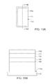
- FIG. 1A shows a top view of a semiconductor structure according to a first embodiment of the present disclosure.
- FIG. 1B shows a cross-sectional view along the section line 1 B- 1 B′ in FIG. 1A .
- FIG. 2A shows a top view of a semiconductor structure according to a second embodiment of the present disclosure.
- FIG. 2B shows a cross-sectional view along the section line 2 B- 2 B′ in FIG. 2A .
- FIG. 3A shows a top view of a semiconductor structure according to a third embodiment of the present disclosure.
- FIG. 3B shows a cross-sectional view along the section line 3 B- 3 B′ in FIG. 3A .
- FIG. 3C shows a schematic view of the power lines between the drain conductive structure 130 and the source conductive structure 140 in FIG. 3A .
- FIG. 4 shows a top view of a semiconductor structure according to a fourth embodiment of the present disclosure.
- FIG. 5A shows a top view of a semiconductor structure according to a fifth embodiment of the present disclosure.
- FIG. 5B shows a cross-sectional view along the section line 5 B- 5 B′ in FIG. 5A .
- FIG. 6A shows a top view of a semiconductor structure according to a sixth embodiment of the present disclosure.
- FIG. 6B shows a cross-sectional view along the section line 6 B- 6 B′ in FIG. 6A .
- FIG. 7A-7C show top views of arrangements of a gate structure, a source conductive structure, a drain conductive structure, and a gate conductive structure of a semiconductor structure according to an embodiment of the present disclosure.
- FIG. 8 shows a top view of a semiconductor device according to an embodiment of the present disclosure.
- FIG. 9 shows a top view of a semiconductor device according to another embodiment of the present disclosure.
- FIGS. 10-17B illustrate a process for manufacturing a semiconductor structure according to one embodiment of the present disclosure.
- FIGS. 18-22B illustrate a process for manufacturing a semiconductor structure according to another embodiment of the present disclosure.
- a semiconductor structure and a manufacturing method of the same are provided.
- the length of a channel area is determined by the distance between a drain conductive structure and a source conductive structure of the semiconductor structure.
- forming a gate structure and defining the range of an active region can be performed in one manufacturing process, such that the whole manufacturing processes can be simplified.
- the embodiments disclosed below are for elaborating the semiconductor structure of the disclosure. However, the descriptions disclosed in the embodiments of the disclosure such as detailed structures, manufacturing procedures, operating procedures, and material selections are for illustration only, not for limiting the scope of protection of the disclosure.
- FIG. 1A shows a top view of a semiconductor structure according to a first embodiment of the present disclosure.
- FIG. 1B shows a cross-sectional view along the section line 1 B- 1 B′ in FIG. 1A .
- Semiconductor structure 100 comprises a substrate 110 , a gate dielectric layer 160 , a gate structure 120 , a drain conductive structure 130 , a source conductive structure 140 , and a gate conductive structure 150 .
- the substrate has a channel area 111 , and the channel area 111 has a length L 1 .
- the gate dielectric layer 160 is formed on the channel area 111
- the gate structure 120 is formed on the gate dielectric layer 160 .
- the drain conductive structure 130 and the source conductive structure 140 are formed on the substrate 110 .
- the drain conductive structure 130 and the source conductive structure 140 penetrate through the gate structure 120 and are electrically connected to the substrate 110 , and the drain conductive structure 130 and the source conductive structure 140 are electrically isolated from the gate structure 120 .
- the gate conductive structure 150 is formed on the gate structure 120 .
- the drain conductive structure 130 and the source conductive structure 140 are separated by a distance D 1 which is equal to the length L 1 of the channel area 111 . That is to say, the distance D 1 between the drain conductive structure 130 and the source conductive structure 140 determines the length L 1 of the channel area 111 .
- a channel length is defined by shallow trench isolation (STI) followed by a gate electrode formation process to define a channel width. And then, processes of photolithography, ion implantation, and formation of spacers are carried out to form a source area and a drain area. Last, an interlayer dielectric (IDL) is formed followed by performing a contact window (contact hole) process.
- IDL interlayer dielectric
- the distance D 1 between the drain conductive structure 130 and the source conductive structure 140 determines the length L 1 of the channel area 111 , such that the length L 1 of the channel area 111 can be controlled and the source conductive structure 130 and the source conductive structure 140 can be defined at the same time.
- the drain conductive structure 130 and the source conductive structure 140 are defined on and through the relatively large gate structure 120 , such that an N ⁇ /P ⁇ region can be defined at the same time while performing the contact process (formation of the drain conductive structure 130 and the source conductive structure 140 ). And then, after a spacer 180 is formed, an N+/P+ region and the contacts are self-aligned formed.
- the formation of the drain conductive structure 130 and the source conductive structure 140 and the definition of the length L 1 of the channel area 111 can be simplified in one module. As a result, the original complicated manufacturing processes can be simplified, the design rules of the gate electrode are relaxed, and the manufacturing costs are reduced.
- the gate structure 120 is located on the same side respect to the drain conductive structure 130 and the source conductive structure 140 .
- the semiconductor structure 100 can comprise an insulating structure 190 formed on the substrate 110 .
- the insulating structure surrounds the substrate 110 , and a part of the surface of the substrate 110 is exposed form the insulating structure 190 .
- a width W 1 of the channel area 111 is equal to a width D 11 of the part of the surface exposed from the insulating structure 190 .
- the range that the insulating structure 190 surrounds defines the width W 1 of the channel area 111 .
- the semiconductor structure 100 can comprise an insulating layer 170 .
- the insulating layer 170 is formed on the substrate 110 and located between the gate conductive structure 150 , the drain conductive structure 130 , and the source conductive structure 140 .
- the insulating layer 10 surrounds the peripheries of the gate conductive structure 150 , the drain conductive structure 130 , and the drain conductive structure 140 .
- the semiconductor structure 100 can comprise a spacer 180 .
- the spacer 180 is formed on a sidewall 130 a of the drain conductive structure 130 and a sidewall 140 a of the source conductive structure 140 .
- the spacer 180 is also formed on a sidewall 150 a of the gate conductive structure 150 .
- the spacer 180 surrounds the peripheries of the gate conductive structure 150 , the drain conductive structure 130 , and the drain conductive structure 140 .
- the material of the spacer 180 comprises an insulating material, such as silicon nitride or silicon oxide.
- the spacer 180 is formed between the gate structure 120 and the drain conductive structure 130 and between the gate structure 120 and the source conductive structure 140 .
- the spacer 180 is such as in direct contact with the gate structure 120 , the drain conductive structure 130 , and the source conductive structure 140 .
- the spacer 180 fully covers the sidewall 130 a of the drain conductive structure 130 and the sidewall 140 a of the source conductive structure 140 .
- the spacer 180 is conformal with the sidewall 130 a of the drain conductive structure 130 and the sidewall 140 a of the source conductive structure 140 .
- the gate structure 120 and the drain conductive structure 130 are spaced apart by only the spacer 180
- the gate structure 120 and the source conductive structure 140 are spaced apart by only the spacer 180 .
- the spacer 180 can prevent the electronic interferences from occurring between the gate structure 120 and the drain conductive structure 130 and between the gate structure 120 and the source conductive structure 140 .
- the shape of the cross-sections of the gate conductive structure 150 , the source conductive structure 130 , and the drain conductive structure 140 is, for example, rectangular.
- the shape of the cross-sections of the gate conductive structure 150 , the source conductive structure 130 , and the drain conductive structure 140 is rectangular, and the length of the drain conductive structure 130 and the drain conductive structure 140 parallel to the width W 1 of the channel area is such as larger than or equal to the width D 11 of the part of the surface of the substrate 110 exposed from the insulating structure 190 .
- the width W 1 of the channel area 111 is determined by the width D 11
- the length L 1 of the channel area 111 is determined by the manufacturing process of the contacts (the drain conductive structure 130 and the source conductive structure 140 ).
- the width W 1 and the length L 1 of the channel area 111 are clearly defined, as such, the semiconductor structure 100 as shown in FIG. 1A has a similar I-V curve to that of a semiconductor structure made by typical manufacturing processes.
- these cross-sections can also be oval-shaped, linear, or have other shapes. However, the shape selections are depending on the conditions applied and are not limited to the shapes aforementioned.
- the substrate 110 is such as a polysilicon substrate.
- the semiconductor structure 100 can comprise a drain area 113 and a source area 115 .
- the drain area 113 and the source area 115 are formed in the substrate 110 .
- the drain area 113 is located adjacent to the drain conductive structure 130
- the source area 115 is located adjacent to the source conductive structure 140 .
- the drain area 113 and the source area 115 can independently comprise a first type doping area 113 a , 115 a , and a second type doping area 113 b , 115 b .
- the first type doping areas 113 a and 115 a are such as located under the drain conductive structure 130 and the source conductive structure 140 , respectively.
- the first type doping areas 113 a and 115 a are such as N ⁇ /P ⁇ doping regions, and the ranges of which are determined by the peripheries of the spacers 180 (e.g. the ranges of the holes, in which the drain conductive structure 130 and the source conductive structure 140 are to be formed, before the spacers 180 are formed).
- the second type doping areas 113 b and 115 b are located between the drain conductive structure 130 and the first doping area and between the source conductive structure 140 and the first doping area, respectively.
- the second type doping areas 113 b and 115 b are such as N+/P+ doping regions, and the ranges of which are determined by the inner edges of the spacers 180 (e.g. the ranges of the drain conductive structure 130 and the source conductive structure 140 ).
- FIG. 2A shows a top view of a semiconductor structure according to a second embodiment of the present disclosure.
- FIG. 2B shows a cross-sectional view along the section line 2 B- 2 B′ in FIG. 2A .
- the gate conductive structure 150 is such as disposed between the drain conductive structure 130 and the source conductive structure 140 .
- the shape of the cross-sections of the gate conductive structure 150 , the source conductive structure 130 , and the drain conductive structure 140 is, for example, rectangular. Similar to the embodiment as shown in FIG. 1A , the width and the length of the channel area 211 are clearly defined, as such, the semiconductor structure 200 as shown in FIG.
- FIG. 2A has an I-V curve similar to that of a semiconductor structure made by typical manufacturing processes.
- these cross-sections can also be oval-shaped, linear, or have other shapes.
- the shape selections are depending on the conditions applied and are not limited to the shapes aforementioned.
- the drain conductive structure 130 and the source conductive structure 140 are separated by a distance D 2 which is equal to a length L 2 of the channel area 211 . That is to say, the distance D 2 between the drain conductive structure 130 and the source conductive structure 140 determines the length L 2 of the channel area 211 .
- semiconductor structure 200 is such as a metal oxide semiconductor (MOS), and the area where the gate structure 120 covers can be an active region A.
- MOS metal oxide semiconductor
- the range of the gate structure 130 defines the active region A of the semiconductor structure 200 .
- the substrate 210 is such as a SOI (silicon on insulator) substrate, comprising a substrate body 215 , a silicon oxide layer 217 , and a silicon layer 219 .
- SOI silicon on insulator
- the substrate selections are depending on the conditions applied and are not limited to the types aforementioned.
- FIG. 3A shows a top view of a semiconductor structure according to a third embodiment of the present disclosure.
- FIG. 3B shows a cross-sectional view along the section line 3 B- 3 B′ in FIG. 3A .
- the shape of the cross-sections of the gate conductive structure 150 , the source conductive structure 130 , and the drain conductive structure 140 is, for example, round.
- FIG. 3C shows a schematic view of the power lines between the drain conductive structure 130 and the source conductive structure 140 in FIG. 3 A.
- the shape of the cross-sections of the source conductive structure 130 and the drain conductive structure 140 is round, the length L 2 ′ and the width W 2 ′ of the channel area 211 ′ are less clearly defined.
- the power lines EL close to the middle of the region between the drain conductive structure 130 and the source conductive structure 140 are substantially straight lines.
- the power lines EL close to the outer sides of the region between the two conductive structures 130 and 140 are curved lines, and the curved lines are bending more outwards when moving away from the region between the two conductive structures 130 and 140 .
- the semiconductor structure 300 as shown in FIG. 3C has an I-V curve different from that of a semiconductor structure made by typical manufacturing processes.
- the I-V curve of the semiconductor structure 300 is similar to that of a plurality of semiconductor structures arranged in parallel, each having channel areas of different lengths and widths.
- the I-V curve of the semiconductor structure 300 is more complicated than that of a semiconductor structure made by typical manufacturing processes.
- the semiconductor structure 300 can be used in suitable logic process after fine characterization.
- FIG. 4 shows a top view of a semiconductor structure according to a fourth embodiment of the present disclosure.
- the gate conductive structure 150 is not disposed between the drain conductive structure 130 and the source conductive structure 140 .
- the gate conductive structure 150 is disposed on the same side of the drain conductive structure 130 and the source conductive structure 140 .
- the drain conductive structure 130 is such as disposed between the gate conductive structure 150 and the source conductive structure 140 .
- the channel area 311 is located in the silicon layer 219 .
- the distance D 3 between the drain conductive structure 130 and the source conductive structure 140 is equal to the length L 3 of the channel area 311 . That is to say, the distance D 3 between the drain conductive structure 130 and the drain conductive structure 140 determines the length L 3 of the channel area 311 .
- FIG. 5A shows a top view of a semiconductor structure according to a fifth embodiment of the present disclosure.
- FIG. 5B shows a cross-sectional view along the section line 5 B- 5 B′ in FIG. 5A .
- the semiconductor structure 400 can comprise an insulating structure 190 .
- the insulating structure 190 is formed on the substrate 110 and surrounding the gate structure 120 .
- the insulating structure 190 and the insulating layer 170 can be formed in different manufacturing processes, having different materials.
- the insulating structure 190 and the insulating layer 170 can also be formed in the same manufacturing process and have the same materials.
- the semiconductor structure 400 is such as a metal oxide semiconductor, and the area surrounded by the insulating structure 190 can be an active region A′.
- the insulating structure 190 defines the active region A′ of the semiconductor structure 400 .
- the sides of the insulating structure 190 adjacent to the periphery of the gate structure 120 are such as conformal with the periphery of the gate structure 120 .
- FIG. 6A shows a top view of a semiconductor structure according to a sixth embodiment of the present disclosure.
- FIG. 6B shows a cross-sectional view along the section line 6 B- 6 B′ in FIG. 6A .
- the drain conductive structure 130 and the source conductive structure 140 are disposed on the two sides of the gate structure 120 and adjacent to the insulating structure 190 .
- the spacer 180 is such as formed between the insulating structure 190 and the drain conductive structure 130 and between the insulating structure 190 and the source conductive structure 140 .
- the spacer 180 is, for example, in direct contact with the insulating structure 190 , the drain conductive structure 130 , and the source conductive structure 140 .
- the channel area 511 is located in the silicon layer 219 .
- the distance D 4 between the drain conductive structure 130 and the source conductive structure 140 is equal to the length L 4 of the channel area 511 . That is to say, the distance D 4 between the drain conductive structure 130 and the source conductive structure 140 determines the length L 4 of the channel area 511 .
- the channel area 511 is located below the gate structure 120 .
- a width of the gate structure 120 is equal to a width W 4 of the channel area 511 .
- the width of the gate structure 120 defines the width W 4 of the channel area 511 .
- FIG. 7A-7C show top views of arrangements of a gate structure, a source conductive structure, a drain conductive structure, and a gate conductive structure of a semiconductor structure according to an embodiment of the present disclosure.
- the channel area of the semiconductor structure 600 a is located below the gate structure 120 .
- the distance D 5 between the drain conductive structure 130 and the source conductive structure 140 is equal to the length L 5 of the channel area.
- the insulating structure 190 is located adjacent to the sidewalls of the gate structure 120 and surrounds the gate structure 120 , and the width D 51 of the gate structure 120 is equal to the width W 5 of the channel area. That to say, the distance D 5 between the drain conductive structure 130 and the source conductive structure 140 determines the length L 5 of the channel area, and the insulating structure 190 defines the width W 5 of the channel area.
- the channel area of the semiconductor structure 600 b is located below the gate structure 120 .
- the distance D 6 between the drain conductive structure 130 and the source conductive structure 140 is equal to the length L 6 of the channel area.
- the width W 6 of the channel area is equal to the width D 61 of the .drain conductive structure 130 and the source conductive structure 140 along a direction vertical to the channel length L 6 . That to say, the distance D 6 between the drain conductive structure 130 and the source conductive structure 140 determines the length L 6 of the channel area, and the width D 61 of the .drain conductive structure 130 and the source conductive structure 140 determines the width W 6 of the channel area.
- the channel area of the semiconductor structure 600 c is located below the gate structure 120 .
- the distance D 7 between the drain conductive structure 130 and the source conductive structure 140 is equal to the length L 7 of the channel area.
- the gate structure 120 is denoted with dashed lines in FIG. 7C .
- the width W 7 of the channel area is equal to the width D 71 of the part of the drain conductive structure 130 and the source conductive structure 140 overlapping the gate structure 120 .
- the distance D 7 between the drain conductive structure 130 and the source conductive structure 140 determines the length L 7 of the channel area
- the width D 71 of the drain conductive structure 130 and the source conductive structure 140 overlapping the gate structure 120 determines the width W 7 of the channel area
- FIG. 8 shows a top view of a semiconductor device according to an embodiment of the present disclosure.
- FIG. 9 shows a top view of a semiconductor device according to another embodiment of the present disclosure.
- Semiconductor device 700 comprises two semiconductor structures 700 a and 700 b disposed adjacent to each other.
- the two drain conductive structures 130 , two source conductive structures 140 , and the two gate conductive structures 150 in the two semiconductor structures 700 a and 700 b are electrically connected through a plurality of metal lines ML.
- the semiconductor structures 600 a and 600 b are spaced apart by the insulating structure 190 for preventing the electronic interferences between each other. As shown in FIG.
- the metal line ML connected to the source conductive structures 140 has a voltage input end V in
- the metal line ML connected to the drain conductive structures 130 has a voltage output end V out
- the voltage input end V in and voltage output end V out are disposed between the two semiconductor structures 700 a and 700 b where the insulating structure 190 is located.
- the gate conductive structures 150 of the two semiconductor structures 700 a and 700 b are connected to working voltage input end V CC and grounding end GND, respectively.
- the metal line ML connected to the source conductive structures 140 has a voltage input end V in
- the metal line ML connected to the drain conductive structures 130 has a voltage output end V out
- the voltage input end V in and voltage output end V out are disposed on the two sides of the two semiconductor structures 800 a and 800 b , respectively.
- the gate conductive structures 150 of the two semiconductor structures 800 a and 800 b are connected to working voltage input end V DD and grounding end GND, respectively.
- the semiconductor structures 700 a / 800 a and the semiconductor structures 700 b / 800 b are such as n type metal oxide semiconductors (NMOS) and p type metal oxide semiconductors (PMOS), respectively, and the semiconductors 700 / 800 are such as inverters, which can be applied on static random access memories (SRAM).
- NMOS n type metal oxide semiconductors
- PMOS p type metal oxide semiconductors
- SRAM static random access memories
- FIGS. 10-17B illustrate a process for manufacturing a semiconductor structure according to one embodiment of the present disclosure.
- a substrate 210 is provided.
- the substrate 210 is such as a SOI substrate, comprising a substrate body 215 , a silicon oxide layer 217 , and a silicon layer 219 .
- the substrate selections are depending on the conditions applied and are not limited to the types aforementioned.
- a gate dielectric layer 160 is formed on the substrate 210 , and a gate structure 120 is formed on the gate dielectric layer 160 .
- the gate structure 120 is formed by such as a mask etching process.
- an insulating layer 170 is formed on the substrate 210 .
- the insulating layer 170 is formed on the gate structure 120 .
- the materials for the gate dielectric layer 160 and the insulating layer 170 are such as silicon oxide, and the material for the gate structure 120 is such as polysilicon.
- the material selections are depending on the conditions applied and are not limited to the materials aforementioned.
- a source conductive structure 140 and a drain conductive structure 130 are formed on the substrate 210 , wherein the source conductive structure 140 and the drain conductive structure 130 penetrate through the gate structure 120 and are electrically connected to the substrate 110 , and the source conductive structure 140 and the drain conductive structure 130 are electrically isolated from the gate structure 120 , and a gate conductive structure 150 is formed on the gate structure 120 .
- the manufacturing method of forming the source conductive structure 140 , the drain conductive structure 130 , and the gate conductive structure 150 such as comprises the following steps.
- FIGS. 12A-12B FIG. 12B shows a cross-sectional view along the section line 102 - 12 B′ in FIG. 12A
- holes C 1 , C 2 , and C 3 are formed in the insulating layer.
- the heights of holes C 1 , C 2 , and C 3 extend from a top surface of the insulating layer 170 to the interface between the insulating layer 170 and the gate structure 120 .
- the holes C 1 , C 2 , and C 3 are formed by such as an etching process.
- FIG. 13A-13B shows a cross-sectional view along the section line 13 B- 13 B′ in FIG. 13A
- a photoresist PR 1 is disposed above the hole C 2
- the gate structure 120 and the gate dielectric layer 160 below the holes C 1 and C 3 are etched, such that the heights of holes C 1 and C 3 extend to the interface of the gate dielectric layer 160 and the substrate 210 .
- holes C 1 and C 3 can extend into the silicon layer 219 .
- FIGS. 14A-14B FIG. 14B shows a cross-sectional view along the section line 14 B- 14 B′ in FIG. 14A
- a spacer 180 is formed the sidewalls of the holes C 1 , C 2 , and C 3 .
- the sidewalls of the holes C 1 , C 2 , and C 3 are fully covered by the spacer 180 .
- FIGS. 15A-15B FIG. 15B shows a cross-sectional view along the section line 15 B- 15 B′ in FIG.
- a conductive material is filled in the holes C 1 , C 2 , and C 3 to form the drain conductive structure 130 , the gate conductive structure 150 , and the source conductive structure 140 in the holes C 1 , C 2 , and C 3 , respectively.
- the drain conductive structure 130 and the source conductive structure 140 penetrate through the gate structure 120 and are isolated from the gate structure 120 by the spacer 180 .
- the material for the spacer 180 is such as silicon nitride, and the conductive material is such as tungsten metal.
- the material selections are depending on the conditions applied and are not limited to the materials aforementioned.
- a semiconductor structure 1300 is formed.
- the semiconductor structure 1300 is such as a metal oxide semiconductor, and the range of the gate structure 120 defines the active region A of the semiconductor structure 1300 .
- the step of forming the gate structure 120 and the step of defining the active region A can be performed in one manufacturing process. As such, a gate does not have to be formed separately after an active region has been defined by disposing an insulating isolation structure. Further, a source contact, a drain contact, and a gate contact would not have to be formed after the insulating isolation structure has been disposed. Therefore, the whole manufacturing processes are simplified with a higher flexibility.
- the substrate 210 has a channel area 1311 , and the distance D 8 between the source conductive structure 140 and the drain conductive structure 130 is equal to the length L 8 of the channel area 1311 .
- the spacer 180 is on the sidewall 140 a of the source conductive structure 140 and the sidewall 130 a of the drain conductive structure 130 .
- the spacer 180 is formed between the gate structure 120 and the source conductive structure 140 and between the gate structure 120 and the drain conductive structure 130 .
- the sidewall 140 a of the source conductive structure 140 and the sidewall 130 a of the drain conductive structure 130 are fully covered by the spacer 180 .
- the insulating layer 170 is between the gate conductive structure 150 , the source conductive structure 140 , and the drain conductive structure 130 .
- an insulating structure 190 is formed on the substrate 210 and surrounding the gate structure 120 .
- the manufacturing method of forming the insulating structure 190 comprises such as the following steps. As shown in FIGS. 16A-16B ( FIG. 16B shows a cross-sectional view along the section line 16 B- 16 B′ in FIG. 16A ), the gate structure 120 and the substrate 210 are etched to expose a surface 210 a of the substrate 210 .
- a photoresist PR 2 is such as disposed on the drain conductive structure 130 , the gate conductive structure 150 , and the source conductive structure 140 , and then, the portions of the insulating layer 170 , the gate structure 120 , the gate dielectric layer 160 , the silicon layer 215 , and the silicon oxide layer 217 uncovered by the photoresist PR 2 are etched, and the exposed surface 210 a is a portion of the silicon oxide layer 217 .
- the region where the photoresist PR 2 is disposed is the predetermined active region.
- FIGS. 17A-17B FIG. 17B shows a cross-sectional view along the section line 17 B- 17 B′ in FIG.
- an insulating structure 190 is formed on the surface 210 a of the substrate.
- the materials for the insulating structure 190 and the materials for the insulating layer 170 may be the same or different.
- the region surrounded by the insulating structure 190 can be the active region A′. As such, the semiconductor structure 400 as shown in FIGS. 5A-5B is formed.
- FIGS. 18-22B illustrate a process for manufacturing a semiconductor structure according to another embodiment of the present disclosure. Please refer to FIGS. 12A-15B and FIGS. 18-22B .
- a gate dielectric layer 160 is formed on a substrate 110 , and a gate structure 120 is formed on the gate dielectric layer 160 .
- an insulating layer 170 is formed on the gate structure 120 , and a barrier layer 185 is formed on the insulating layer 170 .
- the substrate is such as a polysilicon substrate with ion implanted p well, and the material for the barrier layer 175 us such as silicon nitride.
- the material selections are depending on the conditions applied and are not limited to the materials aforementioned.
- an insulating structure 190 is formed on the substrate 100 and surrounding the gate structure 120 .
- the manufacturing method of forming the insulating structure 190 comprises such as the following steps. As shown in FIGS. 19A-19B ( FIG. 19B shows a cross-sectional view along the section line 19 B- 19 B′ in FIG. 19A ), a photoresist PR 2 is disposed on a portion of the surface of the barrier layer 175 , and then, the portions of the barrier layer 175 , the insulating layer 170 , the gate structure 120 , the gate dielectric layer 160 , and the substrate 110 uncovered by the photoresist PR 2 are etched, and a surface 110 a of the substrate 110 is exposed.
- the region where the photoresist PR 2 is disposed is the predetermined active region.
- FIGS. 20A-20B FIG. 20B shows a cross-sectional view along the section line 20 B- 20 B′ in FIG. 20A
- the insulating structure 190 is formed on the surface 110 a of the substrate 110 .
- the photoresist PR 2 and the barrier layer 175 can be removed, and the whole surface of the insulating structure 190 and the insulating layer 170 is planarized by such as a chemical mechanical polishing (CMP) process.
- CMP chemical mechanical polishing
- the materials for the insulating structure 190 and for the insulating layer 170 can be the same or different.
- the region surrounded by the insulating structure 190 can be the predetermined active region.
- a source area 115 and a drain area 113 are formed in the substrate 110 .
- the manufacturing method of forming the source area 115 and the drain area 113 in the substrate 110 comprises such as the following steps. As shown in FIGS. 12A-13B and 21 A- 21 B ( FIG. 21B shows a cross-sectional view along the section line 21 B- 21 B′ in FIG. 21A ), holes C 1 , C 2 , and C 3 are formed in the insulating layer 170 .
- the height of hole C 2 extends from a top surface of the insulating layer 170 to the interface of the insulating layer 170 and the gate structure 120 , and the heights of holes C 1 and C 3 extend to the interface of the gate dielectric layer 160 and the substrate 110 .
- FIGS. 22A-22B FIG. 22B shows a cross-sectional view along the section line 22 B- 22 B′ in FIG.
- a spacer 180 is formed on the sidewalls of the holes C 1 , C 2 , and C 3 , and performing an ion implantation process on the substrate 110 below the holes C 1 and C 3 , respectively, to form second type doping areas 113 b and 115 b .
- the ranges of the second type doping areas 113 b and 115 b are determined by the inner edges of the spacers 180 .
- the first type doping area 113 a and the second type doping area 113 b below the hole C 1 form the drain area 113
- the first type doping area 115 a and the second type doping area 115 b below the hole C 2 form the source area 115 .
- the ranges of the width of the drain area 113 and the width of the source area 115 do not exceed the width of the hole C 1 and the width of the hole C 3 , respectively.
- a source conductive structure 140 and a drain conductive structure 130 are formed on the substrate, and a gate conductive structure 150 is formed on the gate structure 120 .
- the source area 115 is located adjacent to the source conductive structure 140
- the drain area 113 is located adjacent to the drain conductive structure 130 .
- the manufacturing method of forming the source conductive structure 140 , the drain conductive structure 130 , and the gate conductive structure 150 comprises such as the following steps. As shown in FIGS. 14A-15B and 22 A- 22 B, a conductive material is filled in the holes C 1 , C 2 , and C 3 to form the drain conductive structure 130 , the gate conductive structure 150 , and the source conductive structure 140 in the holes C 1 , C 2 , and C 3 , respectively.
- the drain conductive structure 130 and the source conductive structure 140 penetrate through the gate structure 120 and are isolated from the gate structure 120 by the spacer 180 . As such, a semiconductor structure 2000 is formed.
- the semiconductor structure 2000 is such as a metal oxide semiconductor, and the insulating structure 190 defines the active region A′ of the semiconductor structure 2000 .
- the step of etching the gate structure 120 and the step of etching the substrate 110 to define the range of the active region A′ are performed in one manufacturing process.
- a gate does not have to be formed separately after an active region has been defined by disposing an insulating isolation structure.
- a source contact, a drain contact, and a gate contact would not have to be formed after the insulating isolation structure has been disposed. Therefore, the whole manufacturing processes are simplified with a higher flexibility.
- the formation of the interlayer dielectric and the contact window (contact hole) process are performed after the source area and the drain area are formed by an ion implantation process.
- the source area 115 and the drain area 113 are formed after the insulating layer 170 (e.g. interlayer dielectric) and the holes C 1 , C 2 , and C 3 (e.g. contact window process) are formed.
- the number of the manufacturing processes (e.g. thermal treatments) after the ion implantation process is reduced, such that the ranges of ion implantation (e.g. the ranges of the source area 115 and the drain area 113 ) are less influenced by the subsequent processes.
- the ranges of the source area 115 and the drain area 113 can be controlled more precisely, and hence the efficiency of the semiconductor structure 2000 is improved.
Landscapes
- Thin Film Transistor (AREA)
- Insulated Gate Type Field-Effect Transistor (AREA)
Abstract
Description
Claims (20)
Priority Applications (1)
| Application Number | Priority Date | Filing Date | Title |
|---|---|---|---|
| US13/649,232 US8604555B1 (en) | 2012-10-11 | 2012-10-11 | Semiconductor structure and manufacturing method of the same |
Applications Claiming Priority (1)
| Application Number | Priority Date | Filing Date | Title |
|---|---|---|---|
| US13/649,232 US8604555B1 (en) | 2012-10-11 | 2012-10-11 | Semiconductor structure and manufacturing method of the same |
Publications (1)
| Publication Number | Publication Date |
|---|---|
| US8604555B1 true US8604555B1 (en) | 2013-12-10 |
Family
ID=49681524
Family Applications (1)
| Application Number | Title | Priority Date | Filing Date |
|---|---|---|---|
| US13/649,232 Active US8604555B1 (en) | 2012-10-11 | 2012-10-11 | Semiconductor structure and manufacturing method of the same |
Country Status (1)
| Country | Link |
|---|---|
| US (1) | US8604555B1 (en) |
Citations (1)
| Publication number | Priority date | Publication date | Assignee | Title |
|---|---|---|---|---|
| US7696556B2 (en) * | 2005-09-22 | 2010-04-13 | Samsung Electronics Co., Ltd. | Nonvolatile memory devices including high-voltage MOS transistors with floated drain-side auxiliary gates and methods of fabricating the same |
-
2012
- 2012-10-11 US US13/649,232 patent/US8604555B1/en active Active
Patent Citations (1)
| Publication number | Priority date | Publication date | Assignee | Title |
|---|---|---|---|---|
| US7696556B2 (en) * | 2005-09-22 | 2010-04-13 | Samsung Electronics Co., Ltd. | Nonvolatile memory devices including high-voltage MOS transistors with floated drain-side auxiliary gates and methods of fabricating the same |
Similar Documents
| Publication | Publication Date | Title |
|---|---|---|
| US9590038B1 (en) | Semiconductor device having nanowire channel | |
| KR100827666B1 (en) | Semiconductor devices and methods of forming the same | |
| JP5703790B2 (en) | Semiconductor device and manufacturing method thereof | |
| US7902026B2 (en) | Method of fabricating semiconductor device having vertical channel transistor | |
| US11004788B2 (en) | Semiconductor devices and method of manufacturing the same | |
| KR20120124788A (en) | Semiconductor device | |
| KR100541515B1 (en) | Semiconductor device having vertical channel pattern and method of manufacturing same | |
| TWI514577B (en) | Semiconductor component and method of manufacturing same | |
| US11532741B2 (en) | Semiconductor device having vertical DMOS and manufacturing method thereof | |
| KR101827612B1 (en) | Interdigitated capacitor to integrate with flash memory | |
| US20140042518A1 (en) | Semiconductor device and method of manufacturing the same | |
| US20190058035A1 (en) | Semiconductor Device | |
| KR20190083231A (en) | Integrated circuit device | |
| JP6238234B2 (en) | Semiconductor device | |
| US12249648B2 (en) | Semiconductor device having spacer between contract patterns | |
| KR20210028106A (en) | High voltage device with gate extensions | |
| US20120217554A1 (en) | Semiconductor device and method for fabricating the same | |
| CN113611703B (en) | Method for manufacturing semiconductor structure | |
| JP2012015345A (en) | Semiconductor device | |
| US8664072B2 (en) | Source and drain architecture in an active region of a P-channel transistor by tilted implantation | |
| US20140021537A1 (en) | Semiconductor device and method for manufacturing the same | |
| US8604555B1 (en) | Semiconductor structure and manufacturing method of the same | |
| US10134838B2 (en) | Semiconductor device | |
| CN100521238C (en) | Semiconductor device and manufacture thereof | |
| KR102907655B1 (en) | Semiconductor device having upper channels and lower channels and method of manufacturing the same |
Legal Events
| Date | Code | Title | Description |
|---|---|---|---|
| AS | Assignment |
Owner name: MACRONIX INTERNATIONAL CO., LTD., TAIWAN Free format text: ASSIGNMENT OF ASSIGNORS INTEREST;ASSIGNORS:CHEN, SHIH-HUNG;HSIEH, KUANG-YEU;REEL/FRAME:029110/0882 Effective date: 20121008 |
|
| STCF | Information on status: patent grant |
Free format text: PATENTED CASE |
|
| FPAY | Fee payment |
Year of fee payment: 4 |
|
| MAFP | Maintenance fee payment |
Free format text: PAYMENT OF MAINTENANCE FEE, 8TH YEAR, LARGE ENTITY (ORIGINAL EVENT CODE: M1552); ENTITY STATUS OF PATENT OWNER: LARGE ENTITY Year of fee payment: 8 |
|
| MAFP | Maintenance fee payment |
Free format text: PAYMENT OF MAINTENANCE FEE, 12TH YEAR, LARGE ENTITY (ORIGINAL EVENT CODE: M1553); ENTITY STATUS OF PATENT OWNER: LARGE ENTITY Year of fee payment: 12 |