US8603887B2 - Method for depositing a silicon oxide layer of same thickness on silicon and on silicon-germanium - Google Patents
Method for depositing a silicon oxide layer of same thickness on silicon and on silicon-germanium Download PDFInfo
- Publication number
- US8603887B2 US8603887B2 US13/560,348 US201213560348A US8603887B2 US 8603887 B2 US8603887 B2 US 8603887B2 US 201213560348 A US201213560348 A US 201213560348A US 8603887 B2 US8603887 B2 US 8603887B2
- Authority
- US
- United States
- Prior art keywords
- silicon
- layer
- germanium
- forming
- region
- Prior art date
- Legal status (The legal status is an assumption and is not a legal conclusion. Google has not performed a legal analysis and makes no representation as to the accuracy of the status listed.)
- Active
Links
Images


Classifications
-
- H—ELECTRICITY
- H10—SEMICONDUCTOR DEVICES; ELECTRIC SOLID-STATE DEVICES NOT OTHERWISE PROVIDED FOR
- H10D—INORGANIC ELECTRIC SEMICONDUCTOR DEVICES
- H10D64/00—Electrodes of devices having potential barriers
- H10D64/01—Manufacture or treatment
- H10D64/013—Manufacture or treatment of electrodes having a conductor capacitively coupled to a semiconductor by an insulator
- H10D64/01356—Manufacture or treatment of electrodes having a conductor capacitively coupled to a semiconductor by an insulator the insulator being formed after the semiconductor body, the semiconductor being a Group IV material and not being silicon, e.g. Ge, SiGe or SiGeC
-
- H—ELECTRICITY
- H10—SEMICONDUCTOR DEVICES; ELECTRIC SOLID-STATE DEVICES NOT OTHERWISE PROVIDED FOR
- H10D—INORGANIC ELECTRIC SEMICONDUCTOR DEVICES
- H10D30/00—Field-effect transistors [FET]
- H10D30/60—Insulated-gate field-effect transistors [IGFET]
- H10D30/751—Insulated-gate field-effect transistors [IGFET] having composition variations in the channel regions
-
- H—ELECTRICITY
- H10—SEMICONDUCTOR DEVICES; ELECTRIC SOLID-STATE DEVICES NOT OTHERWISE PROVIDED FOR
- H10D—INORGANIC ELECTRIC SEMICONDUCTOR DEVICES
- H10D84/00—Integrated devices formed in or on semiconductor substrates that comprise only semiconducting layers, e.g. on Si wafers or on GaAs-on-Si wafers
- H10D84/01—Manufacture or treatment
- H10D84/0123—Integrating together multiple components covered by H10D12/00 or H10D30/00, e.g. integrating multiple IGBTs
- H10D84/0126—Integrating together multiple components covered by H10D12/00 or H10D30/00, e.g. integrating multiple IGBTs the components including insulated gates, e.g. IGFETs
- H10D84/0165—Integrating together multiple components covered by H10D12/00 or H10D30/00, e.g. integrating multiple IGBTs the components including insulated gates, e.g. IGFETs the components including complementary IGFETs, e.g. CMOS devices
- H10D84/0167—Manufacturing their channels
-
- H—ELECTRICITY
- H10—SEMICONDUCTOR DEVICES; ELECTRIC SOLID-STATE DEVICES NOT OTHERWISE PROVIDED FOR
- H10D—INORGANIC ELECTRIC SEMICONDUCTOR DEVICES
- H10D84/00—Integrated devices formed in or on semiconductor substrates that comprise only semiconducting layers, e.g. on Si wafers or on GaAs-on-Si wafers
- H10D84/01—Manufacture or treatment
- H10D84/02—Manufacture or treatment characterised by using material-based technologies
- H10D84/03—Manufacture or treatment characterised by using material-based technologies using Group IV technology, e.g. silicon technology or silicon-carbide [SiC] technology
- H10D84/038—Manufacture or treatment characterised by using material-based technologies using Group IV technology, e.g. silicon technology or silicon-carbide [SiC] technology using silicon technology, e.g. SiGe
Definitions
- Embodiments relate to the deposition of a silicon oxide layer of the same thickness on silicon regions and silicon-germanium regions (SiGe) of the same substrate. Embodiments more specifically relate to the deposition of a silicon oxide layer forming the gate insulator of P-channel MOS transistors on silicon-germanium and of N-channel MOS transistors on silicon.
- MOS transistors of various types are generally formed, especially MOS transistors with a low operating voltage and MOS transistors with a high operating voltage generally intended to be used for integrated circuit output stages.
- the gate insulator is provided to comprise a silicon oxide layer having a thickness on the order of 5 nm, while this thickness is only on the order of 2 nm for MOS transistors of low operating voltage.
- the silicon oxide is generally formed by thermal growth.
- CMOS Complementary Metal-Oxide-Semiconductor
- SiGe Complementary Metal-Oxide-Semiconductor
- deposition techniques have to be used to form a silicon oxide layer above silicon and above silicon-germanium, especially due to the different oxidation kinetics of Si and SiGe and to the segregation of Ge on the oxidation front.
- FIGS. 1A to 1C illustrate successive steps of the forming of a gate insulator of an N-channel MOS transistor and of a P-channel MOS transistor, on a same substrate, in the case of MOS transistors of high operating voltage.
- FIG. 1A is a cross-section view of the upper portion of a silicon substrate 1 .
- insulation areas 3 delimit the regions where transistors are desired to be formed. Insulation areas 3 , for example, are shallow trenches filled with silicon oxide, commonly designated as STI (“Shallow Trench Insulation”).
- FIG. 1A shows a region 5 on which an N-channel MOS transistor is desired to be formed and the left-hand portion of the drawing shows a region 7 on which a P-channel MOS transistor is desired to be formed.
- region 7 a silicon-germanium to layer 9 which penetrates into silicon substrate 1 and reaches the same level has been formed.
- FIG. 1B illustrates a step of deposition of a silicon oxide layer above the silicon and silicon-germanium regions of substrate 1 .
- a chemical cleaning of the upper surfaces of the Si and SiGe regions with hydrofluoric acid is performed, followed by an oxidizing bath, for example, in a sulfuric peroxide mixture (SPM).
- SPM sulfuric peroxide mixture
- the chemical cleaning is especially used to remove possible contaminants present at the surface of silicon and of silicon-germanium.
- a silicon oxide layer 11 called chemical oxide, having a thickness smaller than 1 nm, generally forms above the Si and SiGe regions.
- a silicon oxide layer 12 is deposited above chemical oxide layer 11 , by low pressure chemical vapor deposition (LPCVD) or rapid thermal chemical vapor deposition (RTCVD).
- LPCVD low pressure chemical vapor deposition
- RTCVD rapid thermal chemical vapor deposition
- FIG. 1C illustrates a step of forming, above silicon oxide layer 12 , a stack 13 of insulating material layers, comprising one or several silicon nitride layers and materials of high dielectric permittivity.
- the forming of this stack, and especially of the silicon nitride layer, implies anneal steps at temperatures approximately ranging from 900 to 1000° C.
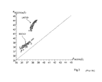
- FIG. 2 is a diagram showing, for various trials, in abscissas, measurements (e SiO2/Si ) of the thickness, in angstroms or tenths of a nanometer, of the silicon oxide layer above the silicon regions and in ordinates, measurements (e SiO2/SiGe ) of the thickness of the silicon oxide layer above the silicon-germanium regions.
- the measurements have been performed once all the insulator forming and anneal steps have been carried out, respectively in the case where silicon oxide layer 12 has been deposited by an LPCVD method and in the case of an RTCVD method.
- the silicon oxide thicknesses on silicon-germanium regions are greater than on silicon regions. It can also be observed that the silicon oxide thickness difference on the silicon and silicon-germanium regions is greater in the case where silicon oxide region 12 has been deposited by an LPCVD method than in the case of an RTCVD method. In the case of a silicon oxide layer 12 deposited by RTCVD, the silicon oxide thickness difference on silicon and silicon-germanium regions is approximately 0.2 nm, against more than 0.5 nm in the case of an LPCVD method.
- Such thickness differences are considered as partly resulting from the initial chemical silicon oxide and partly resulting from the actual deposited silicon oxide.
- the thickness differences of the silicon oxide layer on the silicon regions of N-channel MOS transistors and on the silicon-germanium regions of P-channel MOS transistors raise an to issue, since they result in differences in voltage behavior, leakage currents, and on-state current, and more generally in differences in terms of performance.
- an embodiment provides a method enabling to deposit substantially equal silicon oxide thicknesses on silicon and on silicon-germanium.
- An embodiment provides such a method which enables to use tried and tested silicon oxide deposition techniques.
- An embodiment provides such a method which is simple to implement.
- An embodiment provides such a method which requires no passing through additional equipment with respect to a conventional method of deposition of a silicon oxide layer on a substrate comprising silicon regions and silicon-germanium regions.
- An embodiment provides a method enabling to form a very thin silicon layer, formed at most of a few atomic monolayers, above silicon-germanium regions of a substrate.
- An embodiment provides a method for depositing a silicon oxide layer on a substrate comprising a silicon region and a silicon-germanium region, comprising the steps of: forming a very thin silicon layer having a thickness ranging from 0.1 to 1 nm above silicon-germanium; and depositing a silicon oxide layer on the substrate.
- the deposition of the silicon oxide layer is performed by chemical vapor deposition.
- the deposition of the silicon oxide layer comprises a previous chemical cleaning step.
- the silicon-germanium region is formed of a thin layer having its upper surface substantially at the same level as the upper silicon surface.
- the very thin silicon layer is formed in an epitaxy chamber previously used to form the silicon-germanium region.
- the method comprises the steps of: forming the silicon-germanium region in the presence of a germanium precursor and of a silicon precursor; and stopping the introduction of the germanium precursor to form the very thin silicon layer.
- the temperature is decreased.
- step b) the introduction of the silicon precursor used at step a) is stopped and a silicon precursor containing more chlorinated species than the silicon precursor used as step a) is introduced.
- step b) HCl gas is added.
- the temperature ranges between 550 and 650° C. during the step of forming of the silicon-germanium region, then ranges between 450 and 550° C. during the step of forming of the very thin silicon layer.
- FIGS. 1A to 1C are cross-section views illustrating successive steps of the forming of a gate insulator of an N-channel MOS transistor on silicon and of a P-channel MOS transistor on silicon-germanium;
- FIG. 2 is a diagram illustrating the thickness differences of a silicon oxide layer simultaneously deposited on silicon and on silicon-germanium;
- FIGS. 3A to 3D are cross-section views illustrating successive steps of simultaneous forming of the gate of an N-channel MOS transistor on silicon and of a P-channel MOS transistor on silicon-germanium;
- FIG. 4 is a diagram illustrating a self-limiting process used to form a very thin silicon layer on a silicon-germanium layer.
- FIGS. 1A to 1C and 3 A to 3 D are not to scale.
- FIGS. 3A to 3D illustrate successive steps of the forming of the gate of an N-channel MOS transistor and of a P-channel MOS transistor.
- FIG. 3A is a simplified cross-section view of a portion of a substrate 21 , for example, a silicon substrate, comprising insulation areas 23 delimiting regions in which transistors are desired to be formed.
- the right-hand portion of FIG. 3A shows a region 25 on which an N-channel MOS transistor is desired to be formed, and its left-hand portion shows a region 27 on which a P-channel MOS transistor is desired to be formed.
- Regions 25 have been masked, after which the silicon of substrate 21 has been etched down to a given depth in regions 27 . Then, above the upper surface of substrate 21 , in the etched regions 27 , a silicon-germanium layer 29 covered with a very thin silicon layer 30 has been formed.
- the thickness of the SiGe layer for example ranges between 4 and 10 nm, for example being on the order of 6.5 nm.
- the germanium proportion in the SiGe layer for example ranges between 20 and 40%.
- the thickness of very thin silicon layer 30 covering the SiGe layer approximately ranges from 0.1 to 1 nm, that is, the very thin silicon layer is formed of at most a few atomic monolayers. As shown, the depth of the recess formed in regions 27 may be adjusted so that, after the forming of silicon-germanium layer 29 covered with the very thin silicon layer, the upper surface of the silicon-germanium layer is substantially at the same level as the upper surface of the silicon of regions 25 .
- a next step comprises depositing a silicon oxide layer above the silicon-germanium regions covered with the very thin silicon layer and above the silicon regions of substrate 21 .
- a chemical cleaning of the upper surfaces of the Si and SiGe regions is performed with hydrofluoric acid, followed by an oxidizing bath, for example, in a sulfuric peroxide mixture (SPM).
- SPM sulfuric peroxide mixture
- a very thin silicon oxide layer 31 called chemical oxide, having a thickness smaller than 1 nm, generally forms above the silicon regions and the silicon-germanium regions covered with the very thin silicon layer.
- a silicon oxide layer 32 deposits above chemical oxide layer 31 , generally by low pressure chemical vapor deposition (LPCVD) or rapid thermal chemical vapor deposition (RTCVD).
- LPCVD low pressure chemical vapor deposition
- RTCVD rapid thermal chemical vapor deposition
- the thickness of the silicon oxide layer formed of the chemical silicon oxide layer and of the actual deposited silicon oxide layer for example ranges between 4 and 6 nm, and for example is 5 nm.
- a next step, illustrated in FIG. 3C comprises successively forming, above silicon oxide layer 32 , various layers, for example, a stack 33 of layers of insulating materials, comprising one or several silicon nitride layers and materials of high dielectric permittivity, followed by a stack 35 of layers of conductive materials, comprising at least one layer of a metallic material.
- FIG. 3D illustrates a step of etching of layers 31 , 32 , 33 , and 35 to define gates 36 of the N-channel MOS transistors and gates 37 of the P-channel MOS transistors.
- MOS transistor forming steps especially generally comprising spacer forming steps followed by a source and drain area implantation to step and a contacting step, are carried out, with a possible intermediary siliciding of the source and drain areas.
- a variation of a method of the type described in relation with FIGS. 3A to 3D comprises using hydrofluoric acid only for the chemical cleaning of the upper surfaces of the silicon and silicon-germanium regions before the deposition of silicon oxide layer 32 . During such a chemical cleaning, no silicon oxide layer forms above the silicon regions and the silicon-germanium regions covered with the very thin silicon layer.
- the applicants have measured the thickness of a silicon oxide layer simultaneously deposited on silicon and on silicon-germanium on which a very thin silicon layer has been previously formed, for different thicknesses of the very thin silicon layer. It can be observed that, with a very thin silicon layer having a thickness of 0.3, 0.5, or 0.8 nm, the thickness difference between silicon oxide on silicon and silicon oxide on silicon-germanium is decreased to less than 0.1 nm.
- a method of the type described in relation with FIGS. 3A to 3D enables to deposit substantially equal silicon oxide thicknesses on silicon and on silicon-germanium, by tried and tested silicon oxide deposition methods. Further, the very thin silicon layer covering the silicon-germanium regions being formed at most of a few atomic monolayers, the advantages linked to silicon-germanium for P-channel MOS transistors are kept.
- a silicon-germanium layer is first formed on silicon, preferably above a previously hollowed area of a silicon substrate.
- the silicon-germanium growth is performed in the presence of a germanium precursor, for example, germane (GeH 4 ), and a silicon precursor, for example, silane (SiH 4 ) or dichlorosilane (H 2 SiCl 2 ).
- germanium precursor for example, germane (GeH 4
- SiH 4 silane
- SiCl 2 dichlorosilane
- a silicon layer then grows above the silicon-germanium layer. This growth becomes very slow as soon as the silicon layer reaches a thickness on the order of one atomic monolayer, and slower still if the substrate temperature is decreased, for example to a value ranging between 450 and 550° C.
- the process is thus self-limiting in a way.
- Curve 41 shows, according to the inverse of to temperature (1/T), the growth speed (v cr ) of Si or SiGe on SiGe, and curve 42 shows the growth speed of Si on Si.
- an operating temperature T SiGe enabling to have a SiGe growth speed, v SiGe , allowing a sufficiently fast growth of the SiGe layer, for example, a growth speed on the order of 8 nm/min, is selected. This corresponds to operating point 45 on curve 41 .
- the incoming of the germanium precursor is interrupted.
- a silicon monolayer starts growing, and as soon as this silicon monolayer totally covers the silicon-germanium layer, it is passed to operating point 46 on curve 42 , which characterizes growth speed v Si of silicon on silicon.
- Growth speed v Si is much lower than above-mentioned growth speed v SiGe , for example, on the order of 0.1 nm/min. Given that this growth speed is very small, the process can be stopped after some time while being sure to have a layer of stable thickness from one sample to another.
- the incoming of the germanium precursor may be interrupted and the temperature may be lowered. It is then passed from operating point 45 to operating point 47 on curve 41 and the growth speed of silicon on silicon-germanium v Si1 is on the order of 1 nm/min.
- the silicon-germanium layer is totally coated with silicon, that is, the silicon growth speed (now on silicon) v Si2 becomes very low, lower still than for operating point 46 , for example, on the order of 0.01 nm/min.
- the process regulation then becomes even simpler.
- different silicon precursors may be selected for the silicon-germanium layer growth, and then for the growth of the very thin silicon layer.
- SiGe layer is obtained while the silicon precursor is silane
- a mixture of silane and of HCl gas or dichlorosilane may be used for the growth of the very thin silicon layer.
- a mixture of dichlorosilane and of HCl gas may also be used if the SiGe layer is obtained while the silicon precursor is dichlorosilane.
- An advantage of the method described in relation with FIGS. 3A to 3D is that it requires no passing through additional equipment to form the very thin silicon layer on the silicon-germanium regions of the substrate.
- substrate 21 may be to formed of a thin silicon layer formed on an insulating layer, itself generally formed on a silicon substrate, that is, substrate 21 may be a so-called SOI (silicon-on-insulator) substrate.
- SOI silicon-on-insulator
- insulating areas 23 join the underlying insulating layer.
Landscapes
- Metal-Oxide And Bipolar Metal-Oxide Semiconductor Integrated Circuits (AREA)
- Insulated Gate Type Field-Effect Transistor (AREA)
Abstract
Description
Claims (12)
Applications Claiming Priority (3)
| Application Number | Priority Date | Filing Date | Title |
|---|---|---|---|
| FR1156990A FR2978602A1 (en) | 2011-07-29 | 2011-07-29 | Method for depositing silicon oxide layer on silicon substrate utilized to form gate of e.g. N-channel metal-oxide-semiconductor transistor, involves forming silicon layer over silicon-germanium to deposit oxide layer on substrate |
| FR1156990 | 2011-07-29 | ||
| FR11/56990 | 2011-07-29 |
Publications (2)
| Publication Number | Publication Date |
|---|---|
| US20130072032A1 US20130072032A1 (en) | 2013-03-21 |
| US8603887B2 true US8603887B2 (en) | 2013-12-10 |
Family
ID=44741604
Family Applications (1)
| Application Number | Title | Priority Date | Filing Date |
|---|---|---|---|
| US13/560,348 Active US8603887B2 (en) | 2011-07-29 | 2012-07-27 | Method for depositing a silicon oxide layer of same thickness on silicon and on silicon-germanium |
Country Status (2)
| Country | Link |
|---|---|
| US (1) | US8603887B2 (en) |
| FR (1) | FR2978602A1 (en) |
Families Citing this family (4)
| Publication number | Priority date | Publication date | Assignee | Title |
|---|---|---|---|---|
| US9077029B2 (en) | 2010-02-23 | 2015-07-07 | Samsung Sdi Co., Ltd. | Negative active material for rechargeable lithium battery and rechargeable lithium battery including the same |
| CN110729195A (en) * | 2019-10-28 | 2020-01-24 | 沈阳硅基科技有限公司 | Method for manufacturing planar transistor |
| CN113675135A (en) * | 2020-05-14 | 2021-11-19 | 上海功成半导体科技有限公司 | FD-SOI substrate structure and device structure preparation method |
| CN113224139B (en) * | 2021-04-30 | 2023-05-09 | 长鑫存储技术有限公司 | Semiconductor device and manufacturing method thereof |
Citations (2)
| Publication number | Priority date | Publication date | Assignee | Title |
|---|---|---|---|---|
| US20040070051A1 (en) | 1998-12-24 | 2004-04-15 | Kabushiki Kaisha Toshiba | Semiconductor device and method of manufacturing substrate |
| US20070269963A1 (en) * | 2006-05-19 | 2007-11-22 | International Business Machines Corporation | STRAINED HOT (HYBRID ORIENTATION TECHNOLOGY) MOSFETs |
-
2011
- 2011-07-29 FR FR1156990A patent/FR2978602A1/en not_active Withdrawn
-
2012
- 2012-07-27 US US13/560,348 patent/US8603887B2/en active Active
Patent Citations (2)
| Publication number | Priority date | Publication date | Assignee | Title |
|---|---|---|---|---|
| US20040070051A1 (en) | 1998-12-24 | 2004-04-15 | Kabushiki Kaisha Toshiba | Semiconductor device and method of manufacturing substrate |
| US20070269963A1 (en) * | 2006-05-19 | 2007-11-22 | International Business Machines Corporation | STRAINED HOT (HYBRID ORIENTATION TECHNOLOGY) MOSFETs |
Non-Patent Citations (4)
| Title |
|---|
| Bera L.K, et al., A Dual-Strained CMOS Structure Through Simultaneous Formation of Relaxed and Compressive Strained-SiGe-on-Insulator, IEEE Electron Device Letters, IEEE Service Center, New York, NY, vol. 27, No. 5, May 1, 2006, pp. 350-353, XP001546542. |
| French Search Report and Written Opinion dated Mar. 3, 2012 from corresponding French Application No. 11/56900. |
| Hugh, P.O., Fundamentals of Chemical Vapor Deposition, In: Handbook of Chemical Vapor Deposition: Principles, Technology, and Applications, Jan. 1, 1999, Noyes Publications, Norwich, New Your, XP55023475. |
| Lee C.H., et al., Negative Bias Temperature Instability Characteristics of Strained SiGe pMOSFETS, Electronics Letters, IEE Stevenage, GB, vol. 43, No. 15, Jul. 19, 2007, pp. 835-836 XP006029386. |
Also Published As
| Publication number | Publication date |
|---|---|
| US20130072032A1 (en) | 2013-03-21 |
| FR2978602A1 (en) | 2013-02-01 |
Similar Documents
| Publication | Publication Date | Title |
|---|---|---|
| US7101742B2 (en) | Strained channel complementary field-effect transistors and methods of manufacture | |
| US7494884B2 (en) | SiGe selective growth without a hard mask | |
| US7205206B2 (en) | Method of fabricating mobility enhanced CMOS devices | |
| US7138310B2 (en) | Semiconductor devices having strained dual channel layers | |
| CN100533766C (en) | Semiconductor device based on Si-Ge with high stress liner for enhanced channel carrier mobility | |
| TWI545761B (en) | Semiconductor component and its forming method and P-type gold oxide semi-transistor | |
| US7655987B2 (en) | Method for fabricating ultra-high tensile-stressed film and strained-silicon transistors thereof | |
| US8324038B2 (en) | Method of removing a spacer, method of manufacturing a metal-oxide-semiconductor transistor device, and metal-oxide-semiconductor transistor device | |
| US7605407B2 (en) | Composite stressors with variable element atomic concentrations in MOS devices | |
| KR20060130166A (en) | How to form a semiconductor device with local SOU | |
| KR20060123471A (en) | A method of forming a thin film SOI wafer having high relaxation rate and low stacking defect density | |
| US20090315115A1 (en) | Implantation for shallow trench isolation (STI) formation and for stress for transistor performance enhancement | |
| US8603887B2 (en) | Method for depositing a silicon oxide layer of same thickness on silicon and on silicon-germanium | |
| US20190207013A1 (en) | Controlling gate profile by inter-layer dielectric (ild) nanolaminates | |
| US20080173941A1 (en) | Etching method and structure in a silicon recess for subsequent epitaxial growth for strained silicon mos transistors | |
| US7939396B2 (en) | Base oxide engineering for high-K gate stacks | |
| US20140073111A1 (en) | Method of Forming Isolation Structure | |
| CN110993603A (en) | Semiconductor structure and method of forming the same | |
| WO2005112104A2 (en) | Cmos transistor using high stress liner layer | |
| US8658543B2 (en) | Methods for pFET fabrication using APM solutions | |
| CN110993567B (en) | Semiconductor structure and forming method thereof | |
| US9064888B2 (en) | Forming tunneling field-effect transistor with stacking fault and resulting device | |
| US8390026B2 (en) | Electronic device including a heterojunction region | |
| US9219120B2 (en) | Semiconductor film with adhesion layer and method for forming the same | |
| CN102610530A (en) | Method for producing silicon germanium channel P-channel metal oxide semiconductor (PMOS) with high germanium component |
Legal Events
| Date | Code | Title | Description |
|---|---|---|---|
| AS | Assignment |
Owner name: INTERNATIONAL BUSINESS MACHINES CORPORATION, NEW Y Free format text: ASSIGNMENT OF ASSIGNORS INTEREST;ASSIGNORS:DUTARTRE, DIDIER;CAMPIDELLI, YVES;GOURHANT, OLIVIER;AND OTHERS;SIGNING DATES FROM 20121106 TO 20121203;REEL/FRAME:029399/0068 Owner name: STMICROELECTRONICS S.A, FRANCE Free format text: ASSIGNMENT OF ASSIGNORS INTEREST;ASSIGNORS:DUTARTRE, DIDIER;CAMPIDELLI, YVES;GOURHANT, OLIVIER;AND OTHERS;SIGNING DATES FROM 20121106 TO 20121203;REEL/FRAME:029399/0068 |
|
| STCF | Information on status: patent grant |
Free format text: PATENTED CASE |
|
| AS | Assignment |
Owner name: STMICROELECTRONICS (CROLLES 2) SAS, FRANCE Free format text: CORRECTIVE ASSIGNMENT TO CORRECT THE RECEIVING PARTY DATA PREVIOUSLY RECORDED ON REEL 029399 FRAME 0068. ASSIGNOR(S) HEREBY CONFIRMS THE ASSIGNMENT LISTS STMICROELECTRONICS (CROLLES 2) SAS, BUT THIS ENTITY WAS INADVERTENTLY OMITTED FROM THE RECORDATION COVER SHEET;ASSIGNORS:DUTARTE, DIDIER;CAMPIDELLI, YVES;GOURHANT, OLIVIER;AND OTHERS;SIGNING DATES FROM 20121106 TO 20121203;REEL/FRAME:032118/0388 Owner name: INTERNATIONAL BUSINESS MACHINES CORPORATION, NEW Y Free format text: CORRECTIVE ASSIGNMENT TO CORRECT THE RECEIVING PARTY DATA PREVIOUSLY RECORDED ON REEL 029399 FRAME 0068. ASSIGNOR(S) HEREBY CONFIRMS THE ASSIGNMENT LISTS STMICROELECTRONICS (CROLLES 2) SAS, BUT THIS ENTITY WAS INADVERTENTLY OMITTED FROM THE RECORDATION COVER SHEET;ASSIGNORS:DUTARTE, DIDIER;CAMPIDELLI, YVES;GOURHANT, OLIVIER;AND OTHERS;SIGNING DATES FROM 20121106 TO 20121203;REEL/FRAME:032118/0388 Owner name: STMICROELECTRONICS S.A., FRANCE Free format text: CORRECTIVE ASSIGNMENT TO CORRECT THE RECEIVING PARTY DATA PREVIOUSLY RECORDED ON REEL 029399 FRAME 0068. ASSIGNOR(S) HEREBY CONFIRMS THE ASSIGNMENT LISTS STMICROELECTRONICS (CROLLES 2) SAS, BUT THIS ENTITY WAS INADVERTENTLY OMITTED FROM THE RECORDATION COVER SHEET;ASSIGNORS:DUTARTE, DIDIER;CAMPIDELLI, YVES;GOURHANT, OLIVIER;AND OTHERS;SIGNING DATES FROM 20121106 TO 20121203;REEL/FRAME:032118/0388 |
|
| CC | Certificate of correction | ||
| FPAY | Fee payment |
Year of fee payment: 4 |
|
| MAFP | Maintenance fee payment |
Free format text: PAYMENT OF MAINTENANCE FEE, 8TH YEAR, LARGE ENTITY (ORIGINAL EVENT CODE: M1552); ENTITY STATUS OF PATENT OWNER: LARGE ENTITY Year of fee payment: 8 |
|
| AS | Assignment |
Owner name: STMICROELECTRONICS FRANCE, FRANCE Free format text: CHANGE OF NAME;ASSIGNOR:STMICROELECTRONICS SA;REEL/FRAME:066357/0693 Effective date: 20230126 |
|
| MAFP | Maintenance fee payment |
Free format text: PAYMENT OF MAINTENANCE FEE, 12TH YEAR, LARGE ENTITY (ORIGINAL EVENT CODE: M1553); ENTITY STATUS OF PATENT OWNER: LARGE ENTITY Year of fee payment: 12 |