US8537256B2 - Image pickup device and solid-state image pickup element - Google Patents
Image pickup device and solid-state image pickup element Download PDFInfo
- Publication number
- US8537256B2 US8537256B2 US13/142,021 US201013142021A US8537256B2 US 8537256 B2 US8537256 B2 US 8537256B2 US 201013142021 A US201013142021 A US 201013142021A US 8537256 B2 US8537256 B2 US 8537256B2
- Authority
- US
- United States
- Prior art keywords
- pixels
- light
- image
- optical
- pattern
- Prior art date
- Legal status (The legal status is an assumption and is not a legal conclusion. Google has not performed a legal analysis and makes no representation as to the accuracy of the status listed.)
- Active, expires
Links
Images


Classifications
-
- G—PHYSICS
- G03—PHOTOGRAPHY; CINEMATOGRAPHY; ANALOGOUS TECHNIQUES USING WAVES OTHER THAN OPTICAL WAVES; ELECTROGRAPHY; HOLOGRAPHY
- G03B—APPARATUS OR ARRANGEMENTS FOR TAKING PHOTOGRAPHS OR FOR PROJECTING OR VIEWING THEM; APPARATUS OR ARRANGEMENTS EMPLOYING ANALOGOUS TECHNIQUES USING WAVES OTHER THAN OPTICAL WAVES; ACCESSORIES THEREFOR
- G03B11/00—Filters or other obturators specially adapted for photographic purposes
-
- H—ELECTRICITY
- H04—ELECTRIC COMMUNICATION TECHNIQUE
- H04N—PICTORIAL COMMUNICATION, e.g. TELEVISION
- H04N25/00—Circuitry of solid-state image sensors [SSIS]; Control thereof
-
- H—ELECTRICITY
- H04—ELECTRIC COMMUNICATION TECHNIQUE
- H04N—PICTORIAL COMMUNICATION, e.g. TELEVISION
- H04N25/00—Circuitry of solid-state image sensors [SSIS]; Control thereof
- H04N25/48—Increasing resolution by shifting the sensor relative to the scene
Definitions
- the present invention relates to an image capture device and solid-state image sensor that can increase the resolution of an image to a subpixel precision.
- the resolution of an image can be increased by not just simply increasing the number of pixels of an image sensor but also shifting the pixels of the image sensor with respect to the image that has been captured by an optical system (which is a so-called “pixel shifting technology”).
- the pixel shifting technology may be roughly classified into two types.
- the first type of the pixel shifting technology is spatial shifting, in which the spatial shift is done by arranging a number of pixels in columns and rows on an imaging area of a solid-state image sensor in a shifted pattern so that each row or column of pixels is shifted from its adjacent ones by a half-pixel pitch.
- the second type of the pixel shifting technology is temporal shifting, in which the temporal shift is done by subtly moving mechanically at least one of a solid-state image sensor with a two-dimensional tetragonal arrangement and the optical system.
- Patent Document No. 1 An exemplary fundamental principle for making such spatial pixel shifting by slightly changing the spatial positional of an image is disclosed in Patent Document No. 1, in which such a technique for making pixel shifting with the spatial position of the image changed slightly is applied to a three-panel color camera that uses three image sensors. That color camera adopts an arrangement in which image sensor pixels, representing the color green (G) that will achieve high luminous efficacy to the viewer's eyes, are arranged every other row so as to be horizontally shifted from each other by a half pitch, thereby increasing the resolution in the horizontal direction.
- G color green
- Patent Document No. 2 an arrangement in which pixels are shifted not just horizontally but also vertically is disclosed in Patent Document No. 2.
- photosensitive sections associated with the respective pixels have a diamond shape and are arranged in a winding pattern.
- Patent Document No. 3 an example in which the optical system is subtly moved mechanically with respect to the image sensor is disclosed in Patent Document No. 3, in which a light-transmissive parallel plate is arranged between the image sensor and a lens. By shaking the parallel plate with respect to the optical axis, the optical image produced on the image sensor is moved subtly, thereby increasing the resolution in the direction in which the image is moved subtly.
- Patent Document No. 4 a technique for increasing the resolution by moving the image sensor itself subtly instead of the optical system is disclosed in Patent Document No. 4, in which a piezoelectric element is used as a means for moving the image sensor subtly by a half pixel pitch, thereby attempting to increase the resolution.
- pixels are arranged so as to be shifted from each other by a half pixel pitch both horizontally and vertically or the image sensor is moved subtly by a half pixel pitch both horizontally and vertically, thereby attempting to increase the resolution.
- the photosensitive section had an aperture ratio of 100%, the resolution should be doubled by shifting the pixels by a half pitch.
- the resolution can be certainly roughly doubled but not more than that.
- An image capture device includes a solid-state image sensor with an array of pixels and a number of light-transmitting portions.
- the array is made up of a number of pixels that are arranged two-dimensionally on an imaging area in a first direction and in a second direction that intersects with the first direction.
- the array is divided into a number of unit pixel blocks, each of which is made up of N pixels (where N is an integer that is equal to or greater than two).
- Each light-transmitting portion is provided for an associated one of the pixels and is divided into M areas (where M is an integer that is equal to or greater than two and) that are arranged in the first direction.
- the respective areas have had their optical transmittances set independently of each other.
- the image capture device further includes: an optical system for producing an image on the imaging area of the solid-state image sensor; a shifting section for changing the relative position of the image with respect to the light-transmitting portions in at least one of the first and second directions; and a signal processing section for generating an image, of which the resolution is higher than the resolution that is defined by a pixel pitch of the array of pixels in the first direction, based on the output signals of respective pixels of the solid-state image sensor.
- the optical system includes an optical low-pass filter for decreasing, in the second direction, the resolution of the image to be produced by the optical system, and the shifting section changes the relative position of the image with respect to the light-transmitting portions in the first direction.
- the arrangement pattern of the optical transmittances of the N light-transmitting portions that are provided for the N pixels included in each said unit pixel block is determined by an orthogonal wavelet coefficient.
- the optical system includes a light-transmissive member, one surface of which is tilted with respect to a plane that intersects with the optical axis at right angles, and the shifting section changes the relative position of the image with respect to the light-transmitting portions by moving the light-transmissive member perpendicularly to the optical axis.
- At least all but one of the N light-transmitting portions, which are provided for the N pixels included in each said unit pixel block, have had their optical transmittances set to be either a first transmittance or a second transmittance that is different from the first transmittance.
- the arrangement pattern of the optical transmittances of four light-transmitting portions that are provided for four pixels included in each unit pixel block is selected from the group consisting of a first pattern represented by “1, ⁇ 1, 1, ⁇ 1” and a contrary pattern thereof, a second pattern represented by “ ⁇ 1, 1, 1, ⁇ 1” and a contrary pattern thereof, a third pattern represented by “ ⁇ 1, ⁇ 1, 1, 1” and a contrary pattern thereof, and a fourth pattern in which the optical transmittances of respective areas are set to be a third transmittance that is greater than zero.
- the arrangement pattern of the optical transmittances of four light-transmitting portions that are provided for four pixels included in each unit pixel block is selected from the group consisting of a first pattern represented by “1, ⁇ 1, 1, ⁇ 1”, a second pattern represented by “ ⁇ 1, 1, 1, ⁇ 1” and a contrary pattern thereof, a third pattern represented by “ ⁇ 1, ⁇ 1, 1, 1” and a contrary pattern thereof, and a contrary pattern of the first pattern.
- a solid-state image sensor includes an array of pixels and a number of light-transmitting portions.
- the array is made up of a number of pixels that are arranged two-dimensionally on an imaging area in a first direction and in a second direction that intersects with the first direction.
- the array is divided into a number of unit pixel blocks, each of which is made up of N pixels (where N is an integer that is equal to or greater than two.
- N is an integer that is equal to or greater than two.
- Each of the light-transmitting portions is provided for an associated one of the pixels and divided into M areas (where M is an integer that is equal to or greater than N and) that are arranged in the first direction.
- the respective areas have had their optical transmittances set independently of each other.
- the arrangement pattern of the optical transmittances of N light-transmitting portions that are provided for N pixels included in each unit pixel block vary from one block to another.
- the image capture device and solid-state image sensor of the present invention can obtain a pixel signal with at least a subpixel precision, and therefore, can achieve a higher resolution than what is achieved by a conventional pixel shifting technique.
- FIG. 1 is a block diagram illustrating an overall configuration for an image capture device as a first preferred embodiment of the present invention.
- FIG. 2 is a block diagram illustrating how a lens and a solid-state image sensor are arranged in the first preferred embodiment of the present invention.
- FIG. 3A illustrates an exemplary arrangement of pixels according to the first preferred embodiment of the present invention.
- FIG. 3B illustrates another exemplary arrangement of pixels according to the first preferred embodiment of the present invention.
- Portion (a) of FIG. 4 illustrates a basic arrangement for ND filters in a solid-state image sensor according to the first preferred embodiment of the present invention
- portion (b) of FIG. 4 shows how the signal distribution changes before and after the image is shifted
- portion (c) of FIG. 4 shows the optical transmittances of pixels 30 b and 30 d and their associated pixel signals
- portion (d) of FIG. 4 shows the optical transmittances of pixels 30 a and 30 c and their associated pixel signals.
- FIG. 5 illustrates another basic arrangement for ND filters in a solid-state image sensor according to the first preferred embodiment of the present invention.
- FIG. 6 illustrates still another basic arrangement for ND filters in a solid-state image sensor according to the first preferred embodiment of the present invention.
- Portion (a) of FIG. 7 illustrates a basic arrangement for ND filters in a solid-state image sensor according to a second preferred embodiment of the present invention
- portion (b) of FIG. 7 shows how the signal distribution changes before and after the image is shifted
- portion (c) of FIG. 7 shows the optical transmittances of pixels 30 b and 30 e and their associated pixel signals
- portion (d) of FIG. 7 shows the optical transmittances of pixels 30 a and 30 c at a point in time when the image is shifted horizontally by one pitch and their associated pixel signals
- FIG. 7 shows the optical transmittances of the pixels 30 a and 30 c at a point in time when the image is shifted horizontally by 5/4 pitches and their associated pixel signals; and portion (f) of FIG. 7 shows the optical transmittances of the pixels 30 a and 30 c at a point in time when the image is shifted horizontally by 3/2 pitches and their associated pixel signals.
- Portion (a) of FIG. 8 illustrates a basic arrangement for ND filters in a solid-state image sensor according to a fourth preferred embodiment of the present invention
- portion (b) of FIG. 8 shows how the signal distribution changes before and after the image is shifted
- portion (c) of FIG. 8 shows the optical transmittances of pixels 30 b and 30 e and their associated pixel signals
- portion (d) of FIG. 8 shows the optical transmittances of pixels 30 a and 30 c and their associated pixel signals.
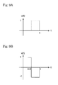
- FIG. 9A is a graph showing a Haar base scaling function.
- FIG. 9B is a graph showing a Haar base wavelet function.
- FIG. 1 is a block diagram illustrating an overall configuration for an image capture device as a first preferred embodiment of the present invention.
- the Image Capture Device of this preferred embodiment is a digital camcorder and includes an image capturing section 100 and a video signal processing section 200 that generates an image signal (such as a video signal) based on the signal supplied from the image capturing section 100 .
- the image capture device is implemented as a camcorder.
- the image capture device may also be a camera that generates only a still picture.
- the image capturing section 100 includes an optical system 11 and a solid-state image sensor 1 (which will be simply referred to herein as an “image sensor”) for converting optical information that has been obtained by the optical system 11 into an electrical signal by photoelectric conversion.
- the optical system 11 includes an optical lens 4 , an optical low-pass filter 2 made of a quartz crystal, and a transparent glass plate 3 , of which the thickness varies according to the distance from its end.
- the transparent glass plate 3 is arranged so as to get moved slightly perpendicularly to the optical axis by an optical system driving section 7 .
- the image capturing section 100 further includes a signal generating and receiving section 5 , which not only generates a fundamental signal to drive this solid-state image sensor 1 but also receives the output signal of the solid-state image sensor 1 and sends it to the signal processing section 10 , and a sensor driving section 6 for driving the image sensor 1 based on the fundamental signal generated by the signal generating and receiving section 5 .
- the sensor driving section 6 may form an integral part of the signal generating and receiving section 5 .
- the optical lens 4 is a known lens and may be a lens unit including multiple lenses.
- the optical low-pass filter 2 is an optical element for reducing a moiré pattern to be caused by a pixel arrangement.
- the image sensor 1 is typically a CCD or CMOS sensor, and may be fabricated by known semiconductor device processing technologies.
- the signal generating and receiving section 5 and the sensor driving section 6 may be implemented as an LSI such as a CCD driver.
- the optical system driving section 7 may be a known piezoelectric element, for example.
- the video signal processing section 200 includes a video signal generating section 9 for generating a video signal by processing the signal supplied from the image capturing section 100 , an image memory section 8 for storing various kinds of data that have been produced while the video signal is being generated, and a video interface section 10 for sending out the video signal thus generated to an external device.
- the video signal generating section 9 is preferably a combination of a hardware component such as a known digital signal processor (DSP) and a software program for use to perform image processing involving the video signal generation.
- DSP digital signal processor
- the video signal generating section 9 and the image memory section 8 are included in the signal processing section of the present invention.
- the image memory section 8 may be a DRAM, for example.
- the image memory section 8 not only stores the signal supplied from the image capturing section 100 but also temporarily retains the image data that has been generated by the video signal generating section 9 or compressed image data. These image data are then output to either a storage medium or a display section (neither is shown) by way of the video interface section 10 .
- the image capture device of this preferred embodiment actually further includes an electronic shutter, a viewfinder, a power supply (or battery), a flashlight and other known components.
- an electronic shutter or a viewfinder
- a power supply or battery
- a flashlight or a flashlight
- this configuration is just an example. Rather, the present invention may also be carried out as any other appropriate combination of known elements except the solid-state image sensor 1 .
- FIG. 2 schematically illustrates how the light that has been transmitted through the optical lens 4 is incident on the image sensor 1 during an exposure process.
- FIG. 2 shown are only the optical lens 4 and the image sensor 1 with illustration of the other components omitted for the sake of simplicity.
- the lens 4 actually often consists of a number of lenses that are arranged in the optical axis direction, the lens 4 shown in FIG. 2 is illustrated as a single lens in a simplified form.
- On the imaging area 1 a of the image sensor 1 arranged two-dimensionally are a number of pixels that form an array of pixels.
- pixels are typically photodiodes, each of which outputs, as a pixel signal, a photoelectrically converted signal representing the intensity of the light received (which will be referred to herein as an “incident light intensity”).
- incident light intensity the intensity of the light received
- FIG. 3A is a plan view illustrating an arrangement of pixels according to a preferred embodiment of the present invention.
- an array of pixels 200 may be made up of a number of pixels that are arranged on the imaging area 1 a to form a tetragonal lattice.
- the array of pixels 200 is divided into a number of unit pixel blocks 40 , each of which consists of four pixels 20 a , 20 b , 20 c and 20 d that are arranged in two columns and two rows.
- the pixels may also have an oblique lattice arrangement as shown in FIG. 3B , instead of the tetragonal lattice arrangement shown in FIG.
- the pixels may be arranged in any form as long as they are arranged two-dimensionally in a first direction and in a second direction that intersects with the first direction.
- the pixel arrangement shown in FIG. 3A is supposed to be adopted.
- the same effect will also be achieved by appropriately changing the directions of ND filters (to be described later) and the directions of shifting the image.
- the XY coordinates shown in FIGS. 3A and 3B will be used, and the X and Y directions will be referred to herein as a “horizontal direction” and a “vertical direction”, respectively, for convenience sake.
- the incoming light is transmitted through the optical lens 4 , the optical glass plate 3 and the optical low-pass filter 2 , imaged on the imaging area 1 a of the solid-state image sensor 1 , and then photoelectrically converted by respective pixels of the solid-state image sensor 1 .
- the optical low-pass filter 2 produces a birefringence of one pixel on the incoming light in the vertical direction of the image, thus decreasing the resolution in that direction.
- the array of pixels 200 of the solid-state image sensor has a basic arrangement consisting of 2 by 2 pixels, each of which is provided with an ND (neutral density) filter that faces that pixel.
- each ND filter is arranged separately from each other in this preferred embodiment, those filters may also be combined into a single filter layer that faces the array of pixels 200 .
- a number of light-transmitting portions have only to be provided so that each of those light-transmitting portions faces an associated one of the pixels.
- each ND filter functions as a single light transmitting section.
- FIG. 4 illustrates a basic pixel arrangement and signal distributions for the solid-state image sensor 1 of this preferred embodiment.
- ND filters 30 a , 30 b , 30 c and 30 d are respectively provided for the pixels 20 a , 20 b , 20 c and 20 d with an aperture ratio of 100% so that each of those filters 30 a through 30 d faces an associated one of the pixel 20 a through 20 d .
- each of the ND filters 30 a through 30 d is made up of four areas, each of which has a width that is one-fourth of one pixel pitch (a) in the horizontal direction.
- each of the four areas thereof is either an area with a relatively high optical transmittance (which will be referred to herein as an “L (light colored area)”) or an area with a relatively low optical transmittance (which will be referred to herein as a “D (dark colored area)”).
- the optical transmittances of the ND filter 30 a have a striped arrangement pattern in which D, L, D and L areas are arranged in this order from left to right in FIG. 4 .
- the optical transmittances of the ND filter 30 b have a striped arrangement pattern in which L, D, D and L areas are arranged in this order from left to right.
- the optical transmittances of the ND filter 30 c have a striped arrangement pattern in which L, L, D and D areas are arranged in this order from left to right. But the ND filter 30 d has no striped pattern and its four areas have the same optical transmittance. Supposing the optical transmittances of the L and D areas are represented by ⁇ (where ⁇ >0) and ⁇ (where 0 ⁇ ), respectively, the optical transmittance of the ND filter 30 d with no striped pattern is set to be ( ⁇ + ⁇ )/2. As a result, the quantities of light to be transmitted through these four ND filters are approximately equal to each other.
- Such a dark- and light-colored pattern is produced based on an orthogonal wavelet transform coefficient that is defined by the Haar base scaling function u(t) shown in FIG. 9A and the Haar base wavelet function v(t) shown in FIG. 9B .
- an orthogonal wavelet transform coefficient that is defined by the Haar base scaling function u(t) shown in FIG. 9A and the Haar base wavelet function v(t) shown in FIG. 9B .
- four items of data provided by four pixels need to be handled per unit pixel block.
- the orthogonal wavelet transform a given group of data may be transformed into a different group of data by performing additions or subtractions on the former group, or the latter group of data may be restored into the former group of data by performing the same arithmetic operations in reverse order.
- the pattern components of these ND filters 30 a , 30 b , 30 c and 30 d may be represented by ( ⁇ 1, 1, ⁇ 1, 1), (1, ⁇ 1, ⁇ 1, 1), (1, 1, ⁇ 1, ⁇ 1), and (1, 1, 1, 1), respectively.
- Their orthogonality can be confirmed by performing the same processing as when the inner product of vectors is calculated. That is to say, if each of these ND filters is supposed to be a vector consisting of four components, then their inner product becomes equal to zero, and it can be seen that they are orthogonal to each other.
- a signal representing the quantity of the light received will be accumulated in respective pixels for a certain amount of time. Then, the accumulated signal is read out from the image sensor 1 , passed through the signal generating and receiving section 5 , and then sent to the image memory section 8 .
- the optical system driving section 7 subtly moves the transparent glass plate 3 perpendicularly to the optical axis (i.e., in the horizontal direction on the image), thereby shifting the image on the imaging area by one pixel pitch in the horizontal direction. After the image has been shifted in this way, the signal will be accumulated again in the respective pixels for the same amount of time.
- the accumulated signal is read out from the image sensor 1 once again and then sent to the image memory section 8 .
- the optical low-pass filter 2 does decrease the resolution in the vertical direction of the image but does not affect the horizontal resolution at all.
- pixel signals to be read will be described with reference to portions (b) through (d) of FIG. 4 .
- the optical low-pass filter 2 As the optical low-pass filter 2 is provided, the quantities of light rays that are entering these ND filters 30 b and 30 d are supposed to be the same.
- Portion (b) of FIG. 4 shows a curve 19 a indicating what degrees of horizontal dependence the signals to be accumulated in the pixels 20 b and 20 c would have were it not for the ND filters.
- signals representing the quantities of light rays that enter the respective areas, of which the width is one fourth of one pixel pitch, are identified by X 1 , X 2 , X 3 , . . . and Xn.
- Portion (b) of FIG. 4 also shows a curve 19 b indicating what degree of horizontal dependence the signals to be accumulated in the pixels 20 a and 20 c will have after the image has been shifted horizontally by one pixel pitch.
- photoelectrically converted signals are read through the ND filters 30 b and 30 d .
- the transmittances at the two outer areas of the ND filter 30 b both ⁇ , while the transmittances at the two inner areas thereof is ⁇ . That is why the signal Sb read out from the pixel 20 b that faces the ND filter 30 b is represented by ⁇ (X 1 +X 4 )+ ⁇ (X 2 +X 3 ).
- the signal Sd obtained through the ND filter 30 d is represented by (X 1 +X 2 +X 3 +X 4 )( ⁇ + ⁇ )/2.
- the image is horizontally shifted to the left by one pixel pitch and photoelectrically converted pixel signals are read out through the ND filters 30 a and 30 c .
- the signal Sa obtained through the ND filter 30 a is represented by ⁇ (X 2 +X 4 )+ ⁇ (X 1 +X 3 ).
- the signal Sc obtained through the ND filter 30 c is represented by ⁇ (X 1 +X 2 )+ ⁇ (X 3 +X 4 ).
- the signals (Y 1 , Y 2 , Y 3 , Y 4 ) obtained by subjecting the signals supplied from the ND filters 30 a through 30 d to these arithmetic operations are wavelet-transformed signals. And if these results are subjected to the same set of additions and subtractions in reverse order, the original signals (X 1 , X 2 , X 3 , X 4 ) can be obtained.
- the image capture device of this preferred embodiment uses four different kinds of ND filters, which are provided for four pixels of the solid-state image sensor 1 so as to face the pixels one to one and which have mutually different arrangement patterns of optical transmittances, thereby increasing the horizontal resolution substantially fourfold.
- each of the three out of those four kinds of ND filters has been divided into four areas, of which the width is one fourth of the horizontal pixel pitch.
- the first ND filter 30 a has a (D, L, D, L) striped pattern
- the second ND filter 30 b has a (L, D, D, L) striped pattern
- the third ND filter 30 c has a (L, L, D, D) striped pattern.
- the fourth ND filter 30 d does not have such a striped pattern but has a uniform transmittance. If the image is horizontally shifted by one pixel pitch across these striped patterns and if the image yet to be shifted and the shifted image are captured, then pixel signals can be obtained from those four areas, each of which has a width that is one fourth of one pixel pitch. That is to say, as pixel signals can be obtained with a subpixel precision, the resolution can be increased much more significantly than in the prior art.
- each pixel is supposed to have an aperture ratio of 100%.
- the aperture ratio may naturally be less than 100%. The same effect will be achieved if the signals are corrected according to the aperture ratio of each of those pixels.
- the arrangement patterns of optical transmittances in the respective ND filters do not have to be the ones that have been described above.
- the arrangement pattern of optical transmittances in any ND filter may also be contrary to the one that has already been described.
- the pattern is “contrary”, then it means that the combination of L and D areas with transmittances ⁇ and ⁇ in the contrary pattern is reverse to that of the given pattern.
- the patterns shown in portion (a) of FIG. 4 may be replaced with the ones shown in FIG.
- FIG. 5 which illustrates an example in which the ND filters 30 a , 30 b , and 30 c are respectively replaced with ND filters 30 e , 30 f , and 30 g with reversed shades. Even with this arrangement, the same result will be obtained by reversing ⁇ and ⁇ in the signal arithmetic operations described above. Although the shades of three ND filters are reversed in this example, only one ND filter or two may have its/their shade reversed, too.
- one pixel is associated with one ND filter in the preferred embodiment described above.
- two pixels may be associated with one ND filter.
- FIG. 6 illustrates such an example in which two pixels 20 a and 20 b are associated with one ND filter 30 h .
- the ND filter 30 h is arranged so as to cover the two pixels 20 a and 20 b .
- the ND filter 30 h is divided into four areas, each of which has a width that is one fourth of one pixel pitch as measured in the X direction.
- the arrangement pattern of optical transmittances of this ND filter 30 h is represented by (D, L, L, D).
- Signals representing the respective intensities of these four areas can be calculated based on two pixel signals that are obtained from the two pixels 20 a and 20 b .
- the resolution in the X direction is a half of the normal resolution.
- the two halves of the ND filter 30 h that respectively face these two pixels 20 a and 20 b function as two different light-transmitting portions. That is why the ND filter 30 h is arranged so that their portions that face the pixels 20 a and 20 b have mutually different arrangement patterns of optical transmittances.
- the optical image is supposed to be shifted by moving the transparent glass plate 3 in the preferred embodiment described above, the image may also be shifted by a different method. That is to say, according to the present invention, any other means may be used as long as those members are arranged so as to change the relative position of the optical image with respect to multiple light-transmitting portions.
- the image can also be shifted even by arranging a transparent glass plate with a uniform thickness that is tilted with respect to the optical axis and by subtly moving that glass plate.
- the same effect can be achieved even by slightly moving such a light-transmissive member, of which the surface is tilted with respect to a plane that intersects with the optical axis at right angles.
- the same effect can also be achieved through signal processing even if the image and the image sensor 1 are fixed but if every ND filter is moved horizontally by one pixel pitch.
- the sensor driving section 6 may have a mechanism for slightly moving the ND filters.
- the optical transmittance of the fourth ND filter 30 d is set to be ( ⁇ + ⁇ )/2 in order to substantially equalize the quantities of light rays striking the respective pixels.
- the horizontal resolution can be four times as high as the normal one, but the vertical resolution decreases to one half of the normal one because the optical low-pass filter 2 is used.
- the vertical pixel pitch may be a half of the normal one. Then, the vertical resolution can be kept approximately as high as the normal resolution even if the optical low-pass filter 2 is used.
- the image capture device of this second preferred embodiment has the same arrangement as the counterpart of the first preferred embodiment described above except the configuration of the ND filters.
- the following description of the second preferred embodiment will be focused on only that difference from the image capture device of the first preferred embodiment and their common features will not be described all over again to avoid redundancies.
- FIG. 7 illustrates a basic pixel arrangement and signal distributions for the solid-state image sensor 1 of this preferred embodiment.
- ND filters 30 a , 30 b , 30 c and 30 e are arranged in stripes for the pixels with an aperture ratio of 100% so that each of those filters 30 a through 30 d faces an associated one of the pixels.
- the ND filter arrangement of the first preferred embodiment is partially changed so that an ND filter 30 e , of which the pattern is contrary to that of the ND filter 30 a , replaces the ND filter 30 d and faces the pixel 20 d .
- the optical transmittances of these shaded patterns are set so that the D portions have a very low optical transmittance (i.e., ⁇ 0), while the L portions have a very high optical transmittance (i.e., ⁇ 1). In this manner, the overall quantity of light transmitted is substantially equalized in every ND filter.
- the transparent glass plate 3 is subtly moved perpendicularly to the optical axis (i.e., in the horizontal direction on the image), thereby shifting the image on the imaging area in the horizontal direction.
- the optical low-pass filter 2 does decrease the resolution in the vertical direction of the image but does not affect the horizontal resolution at all.
- the image is horizontally shifted to three different positions by one pixel pitch, 5/4 pitches and 3/2 pitches, respectively, from its original position in still state. And every time the image is shifted, image signals are generated by photoelectric conversion and read out from the solid-state image sensor 1 .
- the ND filters 30 b and 30 e look at the ND filters 30 b and 30 e .
- the optical low-pass filter 2 is provided, the quantities of light rays that are entering these ND filters 30 b and 30 e are supposed to be the same.
- Portion (b) of FIG. 7 shows a curve 19 a indicating what degrees of horizontal dependence the signals to be accumulated in the pixels 20 b and 20 e would have were it not for the ND filters.
- Portion (b) of FIG. 7 also shows curves 19 b , 19 c and 19 d indicating what degrees of horizontal dependence the signals to be accumulated in the pixels 20 a and 20 e will have after the image has been shifted horizontally by one pixel pitch, 5/4 pitches and 3/2 pitches, respectively.
- photoelectrically converted signals are read through the ND filters 30 b and 30 e .
- the signals obtained through the ND filters 30 b and 30 e are represented by (X 1 +X 4 ) and (X 1 +X 3 ), respectively.
- the image is horizontally shifted by one pixel pitch and photoelectrically converted pixel signals are read out through the ND filters 30 a and 30 c .
- the signals obtained through the ND filters 30 a and 30 c are represented by (X 2 +X 4 ) and (X 1 +X 2 ), respectively.
- the image is horizontally shifted by 5/4 pixel pitches from its original position in still state and photoelectrically converted pixel signals are read out through the ND filters 30 a and 30 c .
- the signals obtained through the ND filters 30 a and 30 c are represented by (X 3 +X 5 ) and (X 2 +X 3 ), respectively.
- the image is horizontally shifted by 3/2 pixel pitches from its original position in still state and photoelectrically converted pixel signals are read out through the ND filters 30 a and 30 c .
- the signals obtained through the ND filters 30 a and 30 c are represented by (X 4 +X 6 ) and (X 3 +X 4 ), respectively.
- the signals Y 1 , Y 2 , Y 3 and Y 4 obtained by performing these arithmetic operations may be the same as their counterparts of the first preferred embodiment described above except the coefficients. It can be said that (Y 1 , Y 2 , Y 3 , Y 4 ) are wavelet transformed signals. And if these results are subjected to the same set of arithmetic operations in reverse order, the original signals (X 1 , X 2 , X 3 , X 4 ) can be obtained.
- Equations (21) through (24) the pixel signals X 1 through X 4 to be obtained from the respective areas, of which the width is one fourth of one pixel pitch, can be calculated:
- X 1 ( Y 1 +Y 2 +Y 3 +Y 4)/4
- X 2 (( Y 1 +Y 2) ⁇ ( Y 3 +Y 4))/4
- X 3 (( Y 1 +Y 3) ⁇ ( Y 2 +Y 4))/4
- X 4 (( Y 1 +Y 4) ⁇ ( Y 2 +Y 3))/4
- the image capture device of this preferred embodiment uses four different kinds of ND filters, which are provided for four pixels of the solid-state image sensor 1 so as to face the pixels one to one and which have mutually different arrangement patterns of optical transmittances, thereby increasing the horizontal resolution substantially fourfold.
- each of those ND filters has been divided into four areas, of which the stripe width is one fourth of the horizontal pixel pitch.
- the first ND filter 30 a has a (D, L, D, L) striped pattern
- the second ND filter 30 b has a (L, D, D, L) striped pattern
- the third ND filter 30 c has a (L, L, D, D) striped pattern
- the fourth ND filter 30 d has a (L, D, L, D) striped pattern.
- the L areas are supposed to have a transmittance of 100% and the D areas are supposed to have a transmittance of 0%.
- these transmittances do not always have to be used because the arithmetic operations described above can be done approximately as defined by those equations if the difference in shade is sufficiently big.
- the arrangement patterns of optical transmittances in the respective ND filters do not have to be the ones that have been described above.
- the arrangement pattern of optical transmittances in any ND filter may also be contrary to the one that has already been described.
- the arrangement pattern of the ND filter 30 e needs to be contrary to that of the ND filter 30 a.
- the image in shifting the image slightly, it is not always necessary to move the transparent glass plate 3 subtly but any other method may be adopted as well.
- the image can also be shifted even by arranging a transparent glass plate with a uniform thickness that is tilted with respect to the optical axis and by subtly moving that glass plate.
- the same effect can be achieved even by slightly moving such a light-transmissive member, of which the surface is tilted with respect to a plane that intersects with the optical axis at right angles.
- the same effect can also be achieved even if the image and the image sensor 1 are fixed but if every ND filter is moved horizontally by one pixel pitch.
- the image capture device of this third preferred embodiment has the same arrangement, and performs the same signal reading process, as its counterpart of the second preferred embodiment described above but different signals are obtained as a result of the arithmetic operations.
- the following description of the third preferred embodiment will be focused on only that difference from the image capture device of the second preferred embodiment and their common features will not be described all over again to avoid redundancies.
- AC signals X 1 through X 4 can be obtained every one fourth pixel pitch as represented by the following Equations (25) through (28):
- X 1 ( Y 2+ Y 3+ Y 4)/4
- X 2 ( Y 2 ⁇ Y 3 ⁇ Y 4)/4
- X 3 ( Y 3 ⁇ Y 2 ⁇ Y 4)/4
- X 4 ( Y 4 ⁇ Y 2 ⁇ Y 3)/4
- the image capture device of this preferred embodiment uses four different kinds of ND filters, which are provided for four pixels of the solid-state image sensor 1 so as to face the pixels one to one and which have mutually different arrangement patterns of optical transmittances, thereby increasing the horizontal resolution substantially fourfold.
- each of those ND filters has been divided into four areas, of which the stripe width is one fourth of the horizontal pixel pitch.
- the first ND filter 30 a has a (D, L, D, L) striped pattern
- the second ND filter 30 b has a (L, D, D, L) striped pattern
- the third ND filter 30 c has a (L, L, D, D) striped pattern
- the fourth ND filter 30 d has a (L, D, L, D) striped pattern.
- the image is horizontally shifted from its initial position by one pixel pitch, 5/4 pixel pitches and then 3/2 pixel pitches, respectively, across these striped patterns and the image yet to be shifted and the shifted images are captured.
- AC pixel signals can be obtained from the respective areas, each of which has a width that is one fourth of one pixel pitch.
- an image with a higher resolution than conventional ones can be obtained even for those AC components.
- an image capture device according to a fourth preferred embodiment of the present invention will be described with reference to FIG. 8 .
- the image capture device of this fourth preferred embodiment uses the same arrangement patterns for the respective areas of the light-transmitting portions as its counterpart of the second preferred embodiment described above but the optical transmittances in the shaded portions of those ND filters, the way of shifting the optical image, and the signal processing method are different from those of the second preferred embodiment described above.
- the following description of the fourth preferred embodiment will be focused on only that difference from the image capture device of the second preferred embodiment and their common features will not be described all over again to avoid redundancies.
- the optical transmittances in the shaded portions of the ND filters are set to be ⁇ and ⁇ (where ⁇ >0 and 0 ⁇ ), respectively, as in the first preferred embodiment described above.
- the way of shifting the optical image and the image capturing process are the same as the ones used in the first preferred embodiment. That is to say, the image produced on the imaging area is horizontally shifted from its original position in still state by one pixel pitch and the pixel signals that have been subjected to photoelectric conversion before and after the image is shifted are read out from the solid-state image sensor 1 .
- FIG. 8 illustrates a basic pixel arrangement and signal distributions for the solid-state image sensor 1 of this preferred embodiment.
- photoelectrically converted signals are read in this preferred embodiment through the ND filters 30 b and 30 e .
- the signals Sb and Se obtained through the ND filters 30 b and 30 e are represented by a (X 1 +X 4 )+ ⁇ (X 2 +X 3 ) and a (X 1 +X 3 ) ⁇ (X 2 +X 4 ), respectively.
- the image is horizontally shifted to the left by one pixel pitch and photoelectrically converted pixel signals are read out through the ND filters 30 a and 30 e .
- X 3 and X 4 are calculated by the following Equations (36) and (37), respectively:
- X 1 ( ⁇ ( ⁇ +2 ⁇ ) Sa +( ⁇ + ⁇ )( Sb+Sc ) ⁇ Se )/2( ⁇ 2 ⁇ 2 ) (34)
- X 2 (( ⁇ +2 ⁇ ) Sa ⁇ ( ⁇ + ⁇ )( Sb ⁇ Sc )+ ⁇ Se )/2( ⁇ 2 ⁇ 2 ) (35)
- X 3 ( ⁇ Sa ⁇ ( ⁇ + ⁇ )( Sb+Sc )+(2 ⁇ + ⁇ ) Se )/2( ⁇ 2 ⁇ 2 ) (36)
- X 4 (( ⁇ 2 ⁇ ) Sa +( ⁇ + ⁇ )( Sb ⁇ Sc ) ⁇ 3 ⁇ Se )/2( ⁇ 2 ⁇ 2 ) (37)
- a high-definition image signal representing an image, of which the horizontal pixel pitch is one fourth of the normal one can be obtained.
- these signal arithmetic operations are just an example. Rather, the arithmetic operations could be carried out in any other procedure as long as the signals X 1 through X 4 can be obtained.
- the image capture device of this preferred embodiment uses four different kinds of ND filters, which are provided for four pixels of the solid-state image sensor 1 so as to face the pixels one to one and which have mutually different arrangement patterns of optical transmittances, thereby increasing the horizontal resolution substantially fourfold.
- each of those ND filters has been divided into four areas, of which the stripe width is one fourth of the horizontal pixel pitch.
- the first ND filter 30 a has a (D, L, D, L) striped pattern
- the second ND filter 30 b has a (L, D, D, L) striped pattern
- the third ND filter 30 c has a (L, L, D, D) striped pattern
- the fourth ND filter 30 d has a (L, D, L, D) striped pattern. If the image is horizontally shifted by one pixel pitch across these striped patterns and if the image yet to be shifted and the shifted images are captured, then pixel signals can be obtained from those four areas, each of which has a width that is one fourth of one pixel pitch. That is to say, as pixel signals can be obtained with a subpixel precision, the resolution can be increased much more significantly than in the prior art.
- each ND filter is supposed to be divided into four striped areas that have the same width in the X direction.
- the effects of the present invention can also be achieved even if these four areas have different widths.
- the respective signals just need to be corrected with a difference in the quantity of the light transmitted, which should be caused by the difference in width between those areas, taken into account.
- the arrangement patterns of optical transmittances of the respective light-transmitting portions do not have to be the ND filter patterns that have been adopted in the first through fourth preferred embodiments of the present invention described above. Rather the optical transmittances of the respective light-transmitting portions may have any other arrangement pattern as long as signals representing the quantities of light rays entering the respective areas of each light-transmitting portion can be obtained. Furthermore, the number of areas per light-transmitting portion does not have to be four, either.
- each unit pixel block just needs to include N pixels (where N is an integer that is equal to or greater than two) and each light-transmitting portion has only to be divided into M areas (where M is an integer that is equal to or greater than two).
- the optical transmittances of the respective areas of each ND filter are set to be ⁇ , ⁇ or ( ⁇ + ⁇ )/2.
- the vertical resolution is decreased, and the image is shifted horizontally, by using the optical low-pass filter 2 of quartz crystal, thereby increasing only the horizontal resolution.
- this measure is taken just to reduce the number of times of shifting the image.
- the optical low-pass filter 2 does not have to be used. Even if the optical low-pass filter 2 is not used and if the image is shifted both horizontally and vertically alike, the same effects as the ones that have already been described for the first through fourth preferred embodiments of the present invention can also be achieved.
- each light-transmitting portion is not always divided into those areas that are arranged in line horizontally but could also be divided into multiple areas that are arranged in line vertically. If the arrangement pattern of the optical transmittances in each light-transmitting portion is such a two-dimensional one, the resolution can be increased not just horizontally but also vertically as well.
- the image capture device and solid-state image sensor of the present invention can be used effectively in every camera that uses a solid-state image sensor, and may be used in digital still cameras, digital camcorders and other consumer electronic cameras and in industrial surveillance cameras, to name just a few.
Landscapes
- Engineering & Computer Science (AREA)
- Multimedia (AREA)
- Signal Processing (AREA)
- Physics & Mathematics (AREA)
- General Physics & Mathematics (AREA)
- Transforming Light Signals Into Electric Signals (AREA)
- Solid State Image Pick-Up Elements (AREA)
- Studio Devices (AREA)
- Blocking Light For Cameras (AREA)
Abstract
Description
- Patent Document No. 1: Japanese Patent Application Laid-Open Publication No. 58-137247
- Patent Document No. 2: Japanese Patent Application Laid-Open Publication No. 60-187187
- Patent Document No. 3: Japanese Patent Application Laid-Open Publication No. 63-284979
- Patent Document No. 4: Japanese Patent Application Laid-Open Publication No. 64-69160
Sa=α(X2+X4)+β(X1+X3) (1)
Sb=α(X1+X4)+β(X2+X3) (2)
Sc=α(X1+X2)+β(X3+X4) (3)
Sd=(X1+X2+X3+X4)(α+β)/2 (4)
Y1=Sd/2(α+β) (5)
Y2=(Sc−Sd)/2(α−β) (6)
Y3=(Sd−Sa)/2(α−β) (7)
Y4=(Sb−Sd)/2(α−β) (8)
Y1=(X1+X2+X3+X4)/4 (9)
Y2=(X1+X2−X3−X4)/4 (10)
Y3=(X1+X2+X3+X4)/4 (11)
Y4=(X1−X2+X3+X4)/4 (12)
X1=Y1+Y2+Y3+Y4 (13)
X2=Y1+Y2−Y3−Y4 (14)
X3=Y1−Y2+Y3−Y4 (15)
X4=Y1−Y2−Y3+Y4 (16)
Y1=(X1+X2+X3+X4) (17)
Y2=(X1+X2)−(X3+X4) (18)
Y3=(X1+X3)−(X2+X4) (19)
Y4=(X1+X4)−(X2+X3) (20)
X1=(Y1+Y2+Y3+Y4)/4 (21)
X2=((Y1+Y2)−(Y3+Y4))/4 (22)
X3=((Y1+Y3)−(Y2+Y4))/4 (23)
X4=((Y1+Y4)−(Y2+Y3))/4 (24)
X1=(Y2+Y3+Y4)/4 (25)
X2=(Y2−Y3−Y4)/4 (26)
X3=(Y3−Y2−Y4)/4 (27)
X4=(Y4−Y2−Y3)/4 (28)
Se=α(X1+X3)+β(X2+X4) (29)
(X1+X3)=(αSe−βSa)/(α2−β2) (30)
(X2+X4)=(αSa−βSe)/(α2−β2) (31)
X3=(αSe−βSa)/(α2−β2)−X1 (32)
X4=(αSa−βSe)/(α2−β2)−X2 (33)
X1=(−(α+2β)Sa+(α+β)(Sb+Sc)−βSe)/2(α2−β2) (34)
X2=((α+2β)Sa−(α+β)(Sb−Sc)+βSe)/2(α2−β2) (35)
X3=(αSa−(α+β)(Sb+Sc)+(2α+β)Se)/2(α2−β2) (36)
X4=((α−2β)Sa+(α+β)(Sb−Sc)−3βSe)/2(α2−β2) (37)
- 1 solid-state image sensor
- 1 a imaging area of solid-state image sensor
- 2 optical low-pass filter
- 3 transparent glass plate
- 4 optical lens
- 5 signal generating and receiving section
- 6 sensor driving section
- 7 optical system driving section
- 8 image memory section
- 9 video signal generating section
- 10 video interface section
- 11 optical system
- 19 a, 19 b, 19 c, 19 d pixel signal
- 20 a, 20 b, 20 c, 20 d pixel
- 30 a, 30 b, 30 c, 30 d, 30 e, 30 f, 30 g, 30 h, 30 i ND filter (light-transmitting portion)
- 40 unit pixel block
- 100 image capturing section
- 200 video signal processing section
Claims (8)
Applications Claiming Priority (3)
| Application Number | Priority Date | Filing Date | Title |
|---|---|---|---|
| JP2009233287 | 2009-10-07 | ||
| JP2009-233287 | 2009-10-07 | ||
| PCT/JP2010/005936 WO2011043051A1 (en) | 2009-10-07 | 2010-10-04 | Image pickup device and solid-state image pickup element |
Publications (2)
| Publication Number | Publication Date |
|---|---|
| US20110254985A1 US20110254985A1 (en) | 2011-10-20 |
| US8537256B2 true US8537256B2 (en) | 2013-09-17 |
Family
ID=43856535
Family Applications (1)
| Application Number | Title | Priority Date | Filing Date |
|---|---|---|---|
| US13/142,021 Active 2031-02-04 US8537256B2 (en) | 2009-10-07 | 2010-10-04 | Image pickup device and solid-state image pickup element |
Country Status (4)
| Country | Link |
|---|---|
| US (1) | US8537256B2 (en) |
| JP (1) | JPWO2011043051A1 (en) |
| CN (1) | CN102177706B (en) |
| WO (1) | WO2011043051A1 (en) |
Cited By (1)
| Publication number | Priority date | Publication date | Assignee | Title |
|---|---|---|---|---|
| US20120019669A1 (en) * | 2010-07-20 | 2012-01-26 | Aptina Imaging Corporation | Systems and methods for calibrating image sensors |
Families Citing this family (9)
| Publication number | Priority date | Publication date | Assignee | Title |
|---|---|---|---|---|
| JP5995084B2 (en) * | 2011-05-19 | 2016-09-21 | パナソニックIpマネジメント株式会社 | Three-dimensional imaging device, imaging device, light transmission unit, and image processing device |
| US10110834B2 (en) * | 2011-11-07 | 2018-10-23 | Raytheon Company | Hadamard enhanced sensors |
| JP6080505B2 (en) * | 2012-11-06 | 2017-02-15 | キヤノン株式会社 | Image blur correction apparatus and control method thereof |
| US9363425B2 (en) * | 2012-12-06 | 2016-06-07 | Semiconductor Components Industries, Llc | Color filter arrangements for fused array imaging systems |
| WO2016200792A1 (en) * | 2015-06-07 | 2016-12-15 | Barrows, Geoffrey, Louis | Localization method and apparatus |
| JP2018157074A (en) * | 2017-03-17 | 2018-10-04 | キヤノン株式会社 | Electronic component, method for manufacturing electronic component, and electronic device |
| US10951825B2 (en) * | 2017-05-23 | 2021-03-16 | Huawei Technologies Co., Ltd. | Image photographing method applied to terminal, and terminal device |
| JP6814762B2 (en) * | 2018-03-16 | 2021-01-20 | 株式会社日立製作所 | Imaging device |
| CN112805992B (en) * | 2018-10-03 | 2024-04-23 | 富士胶片株式会社 | Camera device |
Citations (12)
| Publication number | Priority date | Publication date | Assignee | Title |
|---|---|---|---|---|
| JPS58137247A (en) | 1982-02-10 | 1983-08-15 | Hitachi Ltd | Solid-state image pickup device |
| JPS60187187A (en) | 1984-03-06 | 1985-09-24 | Matsushita Electronics Corp | Solid-state image pickup device and its driving method |
| JPS63284979A (en) | 1987-05-15 | 1988-11-22 | Fujitsu Ltd | Solid-state image pickup element |
| JPS6469160A (en) | 1987-09-10 | 1989-03-15 | Canon Kk | Picture input device |
| US4907074A (en) * | 1985-10-31 | 1990-03-06 | Canon Kabushiki Kaisha | Image pickup apparatus having color separation filters and forming line-sequential luminance and color-difference signals |
| JPH09214988A (en) | 1996-02-05 | 1997-08-15 | Olympus Optical Co Ltd | Still image pickup device |
| US6678000B1 (en) * | 1997-06-27 | 2004-01-13 | Canon Kabushiki Kaisha | High resolution still-image capture apparatus that shifts pixels by plus or minus two-thirds pixel pitch |
| US20040201760A1 (en) * | 2003-01-14 | 2004-10-14 | Motoari Ota | Solid-state imaging element and digital camera |
| US20080007636A1 (en) * | 2006-07-07 | 2008-01-10 | Honeywell International, Inc. | Image sensor that provides raw output comprising compressed data |
| JP2009010847A (en) | 2007-06-29 | 2009-01-15 | Toshiba Corp | Color component interpolation apparatus and method |
| US20090097136A1 (en) * | 2007-10-10 | 2009-04-16 | Olympus Corporation | Optical device and image pickup apparatus using the same optical device |
| US20090127430A1 (en) | 2005-07-26 | 2009-05-21 | Matsushita Electric Industrial Co., Ltd. | Compound-eye imaging apparatus |
Family Cites Families (5)
| Publication number | Priority date | Publication date | Assignee | Title |
|---|---|---|---|---|
| JP3877695B2 (en) * | 2003-04-03 | 2007-02-07 | 松下電器産業株式会社 | Color solid-state imaging device |
| JP2005167874A (en) * | 2003-12-05 | 2005-06-23 | Sanyo Electric Co Ltd | Solid-state imaging device and image signal processing apparatus |
| US7157690B2 (en) * | 2004-03-31 | 2007-01-02 | Matsushita Electric Industrial Co., Ltd. | Imaging device with triangular photodetector array for use in imaging |
| JP2008011467A (en) * | 2006-06-30 | 2008-01-17 | Toshiba Corp | Display panel imaging method and display panel imaging apparatus |
| JP2009116216A (en) * | 2007-11-09 | 2009-05-28 | Seiko Epson Corp | Image display device and image display method |
-
2010
- 2010-10-04 CN CN2010800028948A patent/CN102177706B/en not_active Expired - Fee Related
- 2010-10-04 US US13/142,021 patent/US8537256B2/en active Active
- 2010-10-04 WO PCT/JP2010/005936 patent/WO2011043051A1/en not_active Ceased
- 2010-10-04 JP JP2011501830A patent/JPWO2011043051A1/en active Pending
Patent Citations (13)
| Publication number | Priority date | Publication date | Assignee | Title |
|---|---|---|---|---|
| JPS58137247A (en) | 1982-02-10 | 1983-08-15 | Hitachi Ltd | Solid-state image pickup device |
| JPS60187187A (en) | 1984-03-06 | 1985-09-24 | Matsushita Electronics Corp | Solid-state image pickup device and its driving method |
| US4907074A (en) * | 1985-10-31 | 1990-03-06 | Canon Kabushiki Kaisha | Image pickup apparatus having color separation filters and forming line-sequential luminance and color-difference signals |
| JPS63284979A (en) | 1987-05-15 | 1988-11-22 | Fujitsu Ltd | Solid-state image pickup element |
| JPS6469160A (en) | 1987-09-10 | 1989-03-15 | Canon Kk | Picture input device |
| JPH09214988A (en) | 1996-02-05 | 1997-08-15 | Olympus Optical Co Ltd | Still image pickup device |
| US6678000B1 (en) * | 1997-06-27 | 2004-01-13 | Canon Kabushiki Kaisha | High resolution still-image capture apparatus that shifts pixels by plus or minus two-thirds pixel pitch |
| US20040201760A1 (en) * | 2003-01-14 | 2004-10-14 | Motoari Ota | Solid-state imaging element and digital camera |
| US20090127430A1 (en) | 2005-07-26 | 2009-05-21 | Matsushita Electric Industrial Co., Ltd. | Compound-eye imaging apparatus |
| JP2009225454A (en) | 2005-07-26 | 2009-10-01 | Panasonic Corp | Compound-eye imaging apparatus |
| US20080007636A1 (en) * | 2006-07-07 | 2008-01-10 | Honeywell International, Inc. | Image sensor that provides raw output comprising compressed data |
| JP2009010847A (en) | 2007-06-29 | 2009-01-15 | Toshiba Corp | Color component interpolation apparatus and method |
| US20090097136A1 (en) * | 2007-10-10 | 2009-04-16 | Olympus Corporation | Optical device and image pickup apparatus using the same optical device |
Non-Patent Citations (1)
| Title |
|---|
| International Search Report for corresponding International Application No. PCT/JP2010/005936 mailed Nov. 16, 2010. |
Cited By (2)
| Publication number | Priority date | Publication date | Assignee | Title |
|---|---|---|---|---|
| US20120019669A1 (en) * | 2010-07-20 | 2012-01-26 | Aptina Imaging Corporation | Systems and methods for calibrating image sensors |
| US9066072B2 (en) * | 2010-07-20 | 2015-06-23 | Semiconductor Components Industries, Llc | Systems and methods for calibrating image sensors |
Also Published As
| Publication number | Publication date |
|---|---|
| US20110254985A1 (en) | 2011-10-20 |
| CN102177706B (en) | 2013-11-27 |
| JPWO2011043051A1 (en) | 2013-03-04 |
| CN102177706A (en) | 2011-09-07 |
| WO2011043051A1 (en) | 2011-04-14 |
Similar Documents
| Publication | Publication Date | Title |
|---|---|---|
| US8537256B2 (en) | Image pickup device and solid-state image pickup element | |
| US8514319B2 (en) | Solid-state image pickup element and image pickup apparatus | |
| US8325241B2 (en) | Image pickup apparatus that stores adjacent and contiguous pixel data before integration of same | |
| US8456552B2 (en) | Image pick up unit using a lens array including a plurality of lens sections corresponding to m×n pixels of image pickup device | |
| US8451352B2 (en) | Image pickup apparatus | |
| CN101883215B (en) | Imaging device | |
| CN104041020B (en) | color image sensor | |
| US9041770B2 (en) | Three-dimensional image capture device | |
| RU2490715C1 (en) | Image capturing device | |
| CN104041006B (en) | Image generating method and image forming apparatus | |
| CN104025584B (en) | Color image sensor and camera head | |
| CN103444184B (en) | Color image sensor and imaging device | |
| CN104041009A (en) | Camera element and camera device | |
| US9099369B2 (en) | Solid-state image sensor | |
| US9179127B2 (en) | Three-dimensional imaging device, imaging element, light transmissive portion, and image processing device | |
| WO2013100039A1 (en) | Color imaging element and imaging device | |
| US8860855B2 (en) | Solid-state image sensor with dispersing element that disperses light according to color component, image capture device and signal processing method | |
| CN108886568A (en) | Optical devices | |
| CN103460702B (en) | Color imaging element and imaging device | |
| US20250126370A1 (en) | Image sensor, application processor and image sensing device | |
| JP2007088732A (en) | Solid-state image sensor | |
| JP2015022116A (en) | Imaging device and method for controlling the same |
Legal Events
| Date | Code | Title | Description |
|---|---|---|---|
| AS | Assignment |
Owner name: PANASONIC CORPORATION, JAPAN Free format text: ASSIGNMENT OF ASSIGNORS INTEREST;ASSIGNORS:HIRAMOTO, MASAO;MISAKI, MASAYUKI;TAKIZAWA, TERUYUKI;AND OTHERS;REEL/FRAME:026545/0900 Effective date: 20110614 |
|
| STCF | Information on status: patent grant |
Free format text: PATENTED CASE |
|
| AS | Assignment |
Owner name: PANASONIC INTELLECTUAL PROPERTY CORPORATION OF AMERICA, CALIFORNIA Free format text: ASSIGNMENT OF ASSIGNORS INTEREST;ASSIGNOR:PANASONIC CORPORATION;REEL/FRAME:033033/0163 Effective date: 20140527 Owner name: PANASONIC INTELLECTUAL PROPERTY CORPORATION OF AME Free format text: ASSIGNMENT OF ASSIGNORS INTEREST;ASSIGNOR:PANASONIC CORPORATION;REEL/FRAME:033033/0163 Effective date: 20140527 |
|
| FEPP | Fee payment procedure |
Free format text: PAYOR NUMBER ASSIGNED (ORIGINAL EVENT CODE: ASPN); ENTITY STATUS OF PATENT OWNER: LARGE ENTITY |
|
| FPAY | Fee payment |
Year of fee payment: 4 |
|
| MAFP | Maintenance fee payment |
Free format text: PAYMENT OF MAINTENANCE FEE, 8TH YEAR, LARGE ENTITY (ORIGINAL EVENT CODE: M1552); ENTITY STATUS OF PATENT OWNER: LARGE ENTITY Year of fee payment: 8 |
|
| MAFP | Maintenance fee payment |
Free format text: PAYMENT OF MAINTENANCE FEE, 12TH YEAR, LARGE ENTITY (ORIGINAL EVENT CODE: M1553); ENTITY STATUS OF PATENT OWNER: LARGE ENTITY Year of fee payment: 12 |