US8526262B2 - Multi-channel semiconductor integrated circuit devices for controlling direct current generators and memory systems including the same - Google Patents
Multi-channel semiconductor integrated circuit devices for controlling direct current generators and memory systems including the same Download PDFInfo
- Publication number
- US8526262B2 US8526262B2 US12/878,431 US87843110A US8526262B2 US 8526262 B2 US8526262 B2 US 8526262B2 US 87843110 A US87843110 A US 87843110A US 8526262 B2 US8526262 B2 US 8526262B2
- Authority
- US
- United States
- Prior art keywords
- memory devices
- mbl
- power generation
- integrated circuit
- semiconductor integrated
- Prior art date
- Legal status (The legal status is an assumption and is not a legal conclusion. Google has not performed a legal analysis and makes no representation as to the accuracy of the status listed.)
- Active, expires
Links
Images


Classifications
-
- G—PHYSICS
- G11—INFORMATION STORAGE
- G11C—STATIC STORES
- G11C5/00—Details of stores covered by group G11C11/00
- G11C5/14—Power supply arrangements, e.g. power down, chip selection or deselection, layout of wirings or power grids, or multiple supply levels
-
- G—PHYSICS
- G11—INFORMATION STORAGE
- G11C—STATIC STORES
- G11C5/00—Details of stores covered by group G11C11/00
- G11C5/14—Power supply arrangements, e.g. power down, chip selection or deselection, layout of wirings or power grids, or multiple supply levels
- G11C5/147—Voltage reference generators, voltage or current regulators; Internally lowered supply levels; Compensation for voltage drops
-
- G—PHYSICS
- G11—INFORMATION STORAGE
- G11C—STATIC STORES
- G11C7/00—Arrangements for writing information into, or reading information out from, a digital store
Definitions
- the present inventive concept is directed to semiconductor integrated circuit devices, and more particularly, to multi-channel semiconductor integrated circuit devices including a plurality of memory devices that are independently accessible and related memory systems.
- a multi-channel semiconductor integrated circuit device including at least one memory device may be independently operated for each memory device.
- direct current consumption is relatively large, compared to that of a semiconductor integrated circuit device having the same density.
- a direct current power generator and a node are shared in order to reduce the direct current consumption.
- Some embodiments of the inventive concept provide a multi-channel semiconductor integrated circuit (IC) device independently operating for each channel which may integrally and efficiently control generation of power, and a memory system including the multi-channel semiconductor integrated circuit device.
- IC semiconductor integrated circuit
- a multi-channel semiconductor integrated circuit device including a plurality of memory devices, a detection unit, and a common control unit.
- the plurality of memory devices are independently accessible and each of the plurality of memory devices includes at least one power generation unit and a control unit for controlling an operation of the at least one power generation unit.
- the detection unit detects an operation state of the plurality of memory devices.
- the common control unit commonly controls an operation of the at least one power generation unit of the plurality of memory devices, according to the operation state of the plurality of memory devices detected by the detection unit.
- control unit of each of the plurality of memory devices controls the operation of the at least one power generation unit of a corresponding one of the plurality of memory devices.
- a multi-channel semiconductor integrated circuit device including a plurality of memory devices and a detection unit.
- the plurality of memory devices is independently accessible and each of the plurality of memory devices includes at least one power generation unit.
- the detection unit detects an operation state of the plurality of memory devices.
- the at least one power generation unit of the plurality of memory devices is independently controlled for each of the plurality of memory devices or commonly controlled for the plurality of memory devices, according to a control mode determined by the operation state of the plurality of memory devices detected by the detection unit.
- a memory system including the multi-channel semiconductor integrated circuit device, a controller for controlling the multi-channel semiconductor integrated circuit device, and a plurality of channels, each independently interfacing a corresponding one of the plurality of memory devices and the controller.
- FIG. 1 schematically illustrates the structure of a multi-channel semiconductor integrated circuit device according some embodiments of the present inventive concept.
- FIG. 2A is a block diagram illustrating an operational structure according to some embodiments of the present inventive concept.
- FIG. 2B is a block diagram illustrating an operational structure according to some embodiments of the present inventive concept.
- FIG. 3A is a flowchart illustrating operations according to some embodiments illustrated in FIG. 2A .
- FIG. 3B is a flowchart illustrating operations according to some embodiments illustrated in FIG. 2B .
- FIGS. 4A through 4D illustrate operation states of multi-channel semiconductor integrated circuit devices according to some embodiments illustrated in FIG. 2A .
- FIGS. 5A through 5D illustrate operation states of multi-channel semiconductor integrated circuit devices according to some embodiments illustrated in FIG. 2B .
- FIGS. 6A through 6C are graphs illustrating a supply current of the power generation unit for each of the operation states of the multi-channel semiconductor integrated circuit devices according to some embodiments in FIG. 2A .
- FIG. 7 is a block diagram schematically illustrating the structure of a system including multi-channel semiconductor integrated circuit devices according to some embodiments of the present inventive concept.
- first, second, etc. may be used herein to describe various elements, these elements should not be limited by these terms. These terms are only used to distinguish one element from another. For example, a first signal could be termed a second signal, and, similarly, a second signal could be termed a first signal without departing from the teachings of the disclosure.
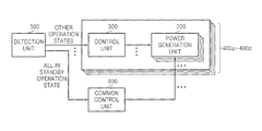
- the multi-channel semiconductor integrated circuit device 100 includes a plurality of, for example, four, memory devices MBL 1 , MBL 2 , MBL 3 , and MBL 4 , a detection unit 500 , and a common control unit 600 .
- the multi-channel semiconductor integrated circuit device 100 may be an integrated circuit device in which the memory devices MBL 1 , MBL 2 , MBL 3 , and MBL 4 are integrated in a single chip.
- Each of the memory devices MBL 1 , MBL 2 , MBL 3 , and MBL 4 separately includes a command and data input/output unit (not shown) so as to be independently accessible.
- the memory devices MBL 1 , MBL 2 , MBL 3 , and MBL 4 respectively, include a plurality of power generation units 200 a 1 , 200 a 2 , 200 a 3 , and 200 a 4 ; 200 b 1 , 200 b 2 , 200 b 3 , and 200 b 4 ; 200 c 1 , 200 c 2 , 200 c 3 , and 200 c 4 ; and 200 d 1 , 200 d 2 , 200 d 3 , and 200 d 4 , control units 300 a , 300 b , 300 c , and 300 d , and bank blocks 400 a , 400 b , 400 c , and 400 d .
- Each of the bank blocks 400 a , 400 b , 400 c , and 400 d may include a memory array (not shown) and a circuit to read/write data with respect to the memory array.
- control units 300 a , 300 b , 300 c , and 300 d control the operation of the power generation units 200 a 1 , 200 a 2 , 200 a 3 , and 200 a 4 ; 200 b 1 , 200 b 2 , 200 b 3 , and 200 b 4 ; 200 c 1 , 200 c 2 , 200 c 3 , and 200 c 4 ; and 200 d 1 , 200 d 2 , 200 d 3 , and 200 d 4 according to the internal voltage of the memory devices MBL 1 , MBL 2 , MBL 3 , and MBL 4 .
- the detection unit 500 detects the operation states of the four memory devices MBL 1 , MBL 2 , MBL 3 , and MBL 4 . For example, the detection unit 500 may detect whether each operation state of the four memory devices MBL 1 , MBL 2 , MBL 3 , and MBL 4 is in an active operation state or a standby operation state.
- the common control unit 600 determines a control mode according to the operation state of the four memory devices MBL 1 , MBL 2 , MBL 3 , and MBL 4 detected by the detection unit 500 .
- the control mode includes an individual control mode and a common control mode.
- the common control mode may be determined by the common control unit 600 .
- the common control unit 600 may control the power generation units 200 a 1 , 200 a 2 , 200 a 3 , and 200 a 4 ; 200 b 1 , 200 b 2 , 200 b 3 , and 200 b 4 ; 200 c 1 , 200 c 2 , 200 c 3 , and 200 c 4 ; and 200 d 1 , 200 d 2 , 200 d 3 , and 200 d 4 for the four memory devices MBL 1 , MBL 2 , MBL 3 , and MBL 4 , and also control the number and/or operation order of the power generation units 200 a 1 , 200 a 2 , 200 a 3 , and 200 a 4 ; 200 b 1 , 200 b 2 , 200 b 3 , and 200 b b
- the common control unit 600 may operate only some of the power generation units 200 a 1 , 200 a 2 , 200 a 3 , and 200 a 4 ; 200 b 1 , 200 b 2 , 200 b 3 , and 200 b 4 ; 200 c 1 , 200 c 2 , 200 c 3 , and 200 c 4 ; and 200 d 1 , 200 d 2 , 200 d 3 , and 200 d 4 of the memory devices MBL 1 , MBL 2 , MBL 3 , and MBL 4 .
- the common control unit 600 may operate only one, for example, the power generation units 200 a 1 , 200 b 1 , 200 c 1 , and 200 d 1 , of the power generation units 200 a 1 , 200 a 2 , 200 a 3 , and 200 a 4 ; 200 b 1 , 200 b 2 , 200 b 3 , and 200 b 4 ; 200 c 1 , 200 c 2 , 200 c 3 , and 200 c 4 ; and 200 d 1 , 200 d 2 , 200 d 3 , and 200 d 4 of the memory devices MBL 1 , MBL 2 , MBL 3 , and MBL 4 .
- the common control unit 600 controls the power generation units 200 a 1 , 200 b 1 , 200 c 1 , and 200 d 1 , to be sequentially operated one by one, so that the multi-channel semiconductor integrated circuit device 100 may be operated.
- the power generation unit 200 a 1 of MBL 1 is first operated so that the multi-channel semiconductor integrated circuit device 100 may be operated.
- the power generation unit 200 b 1 of MBL 2 is operated so that the multi-channel semiconductor integrated circuit device 100 may be operated.
- the power generation unit 200 c 1 of MBL 3 is operated so that the multi-channel semiconductor integrated circuit device 100 may be operated.
- the power generation unit 200 d 1 of MBL 4 is first operated so that the multi-channel semiconductor integrated circuit device 100 may be operated.
- each of the memory devices MBL 1 , MBL 2 , MBL 3 , and MBL 4 may further include standby power generation units 700 a , 700 b , 700 c , and 700 d for supplying power to the four memory devices MBL 1 , MBL 2 , MBL 3 , and MBL 4 .
- the power generation units 200 a 1 , 200 a 2 , 200 a 3 , and 200 a 4 ; 200 b 1 , 200 b 2 , 200 b 3 , and 200 b 4 ; 200 c 1 , 200 c 2 , 200 c 3 , and 200 c 4 ; and 200 d 1 , 200 d 2 , 200 d 3 , and 200 d 4 may be active power generation units that supply power to the memory devices MBL 1 , MBL 2 , MBL 3 , and MBL 4 .
- the standby power generation units 700 a , 700 b , 700 c , and 700 d respectively supply power to the memory devices MBL 1 , MBL 2 , MBL 3 , and MBL 4 .
- the common control unit 600 may control the standby power generation units 700 a , 700 b , 700 c , and 700 d and adjust the number of the operating standby power generation units 700 a , 700 b , 700 c , and 700 d.
- the common control unit 600 operates some of the standby power generation units 700 a , 700 b , 700 c , and 700 d of the memory devices MBL 1 , MBL 2 , MBL 3 , and MBL 4 , thereby operating the multi-channel semiconductor integrated circuit device 100 .
- the common control unit 600 operates only one of the standby power generation units 700 a , 700 b , 700 c , and 700 d of the memory devices MBL 1 , MBL 2 , MBL 3 , and MBL 4 , thereby operating the multi-channel semiconductor integrated circuit device 100 .
- the common control unit 600 controls the standby power generation units 700 a , 700 b , 700 c , and 700 d , to be sequentially operated one by one, so that the multi-channel semiconductor integrated circuit device 100 may be operated.
- the standby power generation unit 700 a of MBL 1 is first operated so that the multi-channel semiconductor integrated circuit device 100 may be operated.
- the standby power generation unit 700 b of MBL 2 is operated so that the multi-channel semiconductor integrated circuit device 100 may be operated.
- the standby power generation unit 700 c of MBL 3 is operated so that the multi-channel semiconductor integrated circuit device 100 may be operated.
- the standby power generation unit 700 d of MBL 4 is first operated so that the multi-channel semiconductor integrated circuit device 100 may be operated.
- FIG. 2A a block diagram illustrating details of multi-channel semiconductor integrated circuit device 100 according to some embodiments of the present inventive concept will be discussed.
- the detection unit 500 detects the operation state of the multi-channel semiconductor integrated circuit device 100 .
- each of the four control units 300 controls the power generation unit 200 for each of the memory devices MBL 1 , MBL 2 , MBL 3 , and MBL 4 .
- the common control unit 600 commonly controls the power generation unit 200 of each of the four memory devices MBL 1 , MBL 2 , MBL 3 , and MBL 4 .
- the memory devices MBL 1 , MBL 2 , MBL 3 , and MBL 4 further include a standby power generation unit 700 that supplies power to the memory devices MBL 1 , MBL 2 , MBL 3 , and MBL 4 when the memory devices MBL 1 , MBL 2 , MBL 3 , and MBL 4 are in the standby operation state.
- a standby power generation unit 700 that supplies power to the memory devices MBL 1 , MBL 2 , MBL 3 , and MBL 4 when the memory devices MBL 1 , MBL 2 , MBL 3 , and MBL 4 are in the standby operation state.
- the detection unit 500 detects the operation state of the multi-channel semiconductor integrated circuit device 100 .
- each control unit 300 of the four memory devices MBL 1 , MBL 2 , MBL 3 , and MBL 4 controls the power generation unit 200 and the standby power generation unit 700 of each of the memory devices MBL 1 , MBL 2 , MBL 3 , and MBL 4 .
- the common control unit 600 When all of the four memory devices MBL 1 , MBL 2 , MBL 3 , and MBL 4 are determined to be in the standby operation state, the common control unit 600 commonly controls the four standby power generation units 700 of the four memory devices MBL 1 , MBL 2 , MBL 3 , and MBL 4 .
- the detection unit 500 determines whether the four memory devices MBL 1 , MBL 2 , MBL 3 , and MBL 4 are all in the standby operation state.
- the common control unit 600 controls all power generation units 200 of the four memory devices MBL 1 , MBL 2 , MBL 3 , and MBL 4 (S 200 ).
- control unit 300 controls all power generation units 200 of the four memory devices MBL 1 , MBL 2 , MBL 3 , and MBL 4 (S 300 ).
- the detection unit 500 determines whether the four memory devices MBL 1 , MBL 2 , MBL 3 , and MBL 4 are all in the standby operation state.
- the common control unit 600 controls the four standby power generation units 700 (S 20 ).
- control unit 300 controls the power generation unit 200 and the standby power generation unit 700 of each of the four memory devices MBL 1 , MBL 2 , MBL 3 , and MBL 4 (S 30 ).
- FIG. 4A through 4D operation states of the multi-channel semiconductor integrated circuit device 100 according to FIG. 2A will be discussed.
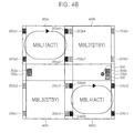
- FIG. 4A the operation state of the multi-channel semiconductor integrated circuit device 100 in which MBL 1 is in the active operation state and MBL 2 -MBL 4 are in the standby operation state.
- FIG. 4B the operation state of the multi-channel semiconductor integrated circuit device 100 in which MBL 1 and MBL 4 are in the active operation state and MBL 2 and MBL 3 are in the standby operation state.
- the multi-channel semiconductor integrated circuit device 100 is shown in which MBL 1 -MBL 4 are all in the active operation state.
- the multi-channel semiconductor integrated circuit device 100 is shown in which MBL 1 -MBL 4 are all in the standby operation state.
- control units 300 a , 300 b , 300 c , and 300 d of the four memory devices MBL 1 , MBL 2 , MBL 3 , and MBL 4 control the power generation units 200 a 1 , 200 a 2 , 200 a 3 , and 200 a 4 ; 200 b 1 , 200 b 2 , 200 b 3 , and 200 b 4 ; 200 c 1 , 200 c 2 , 200 c 3 , and 200 c 4 ; and 200 d 1 , 200 d 2 , 200 d 3 , and 200 d 4 of the memory devices MBL 1 , MBL 2 , MBL 3 , and MBL 4 .
- the common control unit 600 controls the power generation units 200 a 1 , 200 a 2 , 200 a 3 , and 200 a 4 ; 200 b 1 , 200 b 2 , 200 b 3 , and 200 b 4 ; 200 c 1 , 200 c 2 , 200 c 3 , and 200 c 4 ; and 200 d 1 , 200 d 2 , 200 d 3 , and 200 d 4 of the memory devices MBL 1 , MBL 2 , MBL 3 , and MBL 4 .
- FIG. 4 the common control unit 600 controls the power generation units 200 a 1 , 200 a 2 , 200 a 3 , and 200 a 4 ; 200 b 1 , 200 b 2 , 200 b 3 , and 200 b 4 ; 200 c 1 , 200 c 2 , 200 c 3 , and 200 c 4 ; and 200 d 1 , 200 d 2 , 200 d 3 , and 200 d 4 of the memory devices MBL
- the power generation units 200 a 1 , 200 b 1 , 200 c 1 , and 200 d 1 of the memory devices MBL 1 , MBL 2 , MBL 3 , and MBL 4 are sequentially operated, for example, in order of the power generation units 200 a 1 , 200 b 1 , 200 c 1 , and 200 d 1 , so that the multi-channel semiconductor integrated circuit device 100 may be operated.
- FIGS. 5A-5D the operation states of the multi-channel semiconductor integrated circuit device 100 according to FIG. 2B will be discussed.
- the multi-channel semiconductor integrated circuit device 100 is shown in which MBL 1 is in the active operation state and MBL 2 -MBL 4 are in the standby operation state.
- the multi-channel semiconductor integrated circuit device 100 is shown in which MBL 1 and MBL 4 are in the active operation state and MBL 2 and MBL 3 are in the standby operation state.
- FIG. 5C the operation state of the multi-channel semiconductor integrated circuit device 100 in which MBL 1 -MBL 4 are all in the active operation state.
- FIG. 5D the operation state of the multi-channel semiconductor integrated circuit device 100 in which MBL 1 -MBL 4 are all in the standby operation state.
- the control units 300 a , 300 b , 300 c , and 300 d of the four memory devices MBL 1 , MBL 2 , MBL 3 , and MBL 4 control the power generation units 200 a 1 , 200 a 2 , 200 a 3 , and 200 a 4 ; 200 b 1 , 200 b 2 , 200 b 3 , and 200 b 4 ; 200 c 1 , 200 c 2 , 200 c 3 , and 200 c 4 ; and 200 d 1 , 200 d 2 , 200 d 3 , and 200 d 4 and the standby power generation units 700 a , 700 b , 700 c , and 700 d of the memory devices MBL 1 , MBL 2 , MBL 3 , and MBL 4 .
- the common control unit 600 controls the standby power generation units 700 a , 700 b , 700 c , and 700 d of the memory devices MBL 1 , MBL 2 , MBL 3 , and MBL 4 .
- the standby power generation units 700 a , 700 b , 700 c , and 700 d of the memory devices MBL 1 , MBL 2 , MBL 3 , and MBL 5 are sequentially operated, for example, in order of the standby power generation units 700 a , 700 b , 700 c , and 700 d , so that the multi-channel semiconductor integrated circuit device 100 may be operated.
- FIGS. 6A-6C graphs showing supply current of the power generation units 200 a 1 , 200 a 2 , 200 a 3 , and 200 a 4 ; 200 b 1 , 200 b 2 , 200 b 3 , and 200 b 4 ; 200 c 1 , 200 c 2 , 200 c 3 , and 200 c 4 ; and 200 d 1 , 200 d 2 , 200 d 3 , and 200 d 4 for each of the operation states of the multi-channel semiconductor integrated circuit device 100 according to FIG. 2A will be discussed.
- the horizontal axis denotes time and the vertical axis denotes supply current.
- the fourth graph corresponds to a graph of the current supplied by the power generation unit 200 a 1 of FIG. 1 .
- the first to third graphs correspond to graphs of the current supplied by the power generation units 200 b 1 , 200 c 1 , and 200 d 1 .
- MBL 1 is in the active operation state and MBL 2 -MBL 4 are in the standby operation state.
- the current needed in the active state is supplied by the power generation units 200 a 1 , 200 a 2 , 200 a 3 , and 200 a 4 of MBL 1 . Since the power generation units 200 a 1 , 200 a 2 , 200 a 3 , and 200 a 4 of MBL 1 sequentially supply the current needed in the active operation state, as illustrated in FIG. 6A , the power generation units 200 a 1 , 200 a 2 , 200 a 3 , and 200 a 4 supply a predetermined current to MBL 1 with a time difference.
- MBL 1 -MBL 4 are all in the active operation state.
- the current needed in the active state is supplied by each of the power generation units 200 a 1 , 200 a 2 , 200 a 3 , and 200 a 4 ; 200 b 1 , 200 b 2 , 200 b 3 , and 200 b 4 ; 200 c 1 , 200 c 2 , 200 c 3 , and 200 c 4 ; and 200 d 1 , 200 d 2 , 200 d 3 , and 200 d 4 of the MBL 1 -MBL 4 .
- MBL 1 -MBL 4 are all in the standby operation state.
- the current needed in the standby state is supplied by the power generation units 200 a 1 , 200 b 1 , 200 c 1 , and 200 d 1 of MBL 1 -MBL 4 . Since the power generation units 200 a 1 , 200 b 1 , 200 c 1 , and 200 d 1 of MBL 1 -MBL 4 sequentially supply the current needed in the standby operation state, as illustrated in FIG. 6C , the power generation units 200 a 1 , 200 b 1 , 200 c 1 , and 200 d 1 supply a predetermined current to MBL 1 -MBL 4 with a time difference.
- FIG. 7 a block diagram schematically illustrating the structure of a system 1 including the multi-channel semiconductor integrated circuit device 100 according to some embodiments of the present inventive concept.
- the system 1 according to the present exemplary embodiment includes the multi-channel semiconductor integrated circuit device 100 and a controller 10 .
- the system 1 of FIG. 7 may be implemented as a memory card.
- the controller 10 may be configured to communicate with an external device(for example, a host) via any one of USB(Universal Serial Bus), MMC(MultiMediaCard) interface, PCI-E(PCI-Express) interface, SATA(Serial AT Attachment), PATA(Parallel AT Attachment), SCSI(Small Computer System Interface), ESDI(Enhanced Small Disk Interface), and IDE(Integrated Drive Electronics) interface, etc.
- the multi-channel semiconductor integrated circuit device 100 may be used as a data memory device or a code memory device for mobile devices such as a cellular phone, a PDA(Personal digital assistant), a digital camera, a portable game console, and a MP3 player.
- the multi-channel semiconductor integrated circuit device 100 may be used as a data memory device or a code memory device for mobile devices such as a cellular phone, a PDA(Personal digital assistant), a digital camera, a portable game console, and a MP3 player. Furthermore, the multi-channel semiconductor integrated circuit device 100 may be used as a data memory device or a code memory device for home application system such as a computer, a HDTV(High-definition television), a DVD(‘Digital Versatile Disc’ or ‘Digital Video Disc’), a router, and a GPS(Global Positioning System)
- the multi-channel semiconductor integrated circuit device 100 and/or the controller 10 may be packed in various types of packages.
- the various packages may include PoP(Package on Package), Ball grid arrays(BGAs), Chip scale packages(CSPs), Plastic Leaded Chip Carrier(PLCC), Plastic Dual In-Line Package(PDIP), Die in Waffle Pack, Die in Wafer Form, Chip On Board(COB), Ceramic Dual In-Line Package(CERDIP), Plastic Metric Quad Flat Pack(MQFP), Thin Quad Flatpack(TQFP), Small Outline(SOIC), Shrink Small Outline Package(SSOP), Thin Small Outline(TSOP), Thin Quad Flatpack(TQFP), System In Package(SIP), Multi Chip Package(MCP), Wafer-level Fabricated Package(WFP), Wafer-Level Processed Stack Package(WSP).
- PoP Package on Package
- BGAs Ball grid arrays
- CSPs Chip scale packages
- PLCC Plastic Leaded Chip Carrier
- PDIP Plastic Dual In-Line Package
- PDIP
- the multi-channel semiconductor integrated circuit device including a plurality of channels that are independently operated is integrally controlled, deviation in the charge consumption amount according to the active timing of each channel may be reduced. Furthermore, during the standby operation, the standby voltage ripple and standby current may be reduced.
Landscapes
- Engineering & Computer Science (AREA)
- Power Engineering (AREA)
- Static Random-Access Memory (AREA)
- Power Sources (AREA)
- Semiconductor Integrated Circuits (AREA)
Abstract
Description
Claims (16)
Applications Claiming Priority (2)
| Application Number | Priority Date | Filing Date | Title |
|---|---|---|---|
| KR10-2009-0091170 | 2009-09-25 | ||
| KR1020090091170A KR20110033611A (en) | 2009-09-25 | 2009-09-25 | Multi-channel semiconductor integrated circuit device for controlling the power generation unit according to the control mode and a memory system including the same |
Publications (2)
| Publication Number | Publication Date |
|---|---|
| US20110075501A1 US20110075501A1 (en) | 2011-03-31 |
| US8526262B2 true US8526262B2 (en) | 2013-09-03 |
Family
ID=43780249
Family Applications (1)
| Application Number | Title | Priority Date | Filing Date |
|---|---|---|---|
| US12/878,431 Active 2031-09-06 US8526262B2 (en) | 2009-09-25 | 2010-09-09 | Multi-channel semiconductor integrated circuit devices for controlling direct current generators and memory systems including the same |
Country Status (2)
| Country | Link |
|---|---|
| US (1) | US8526262B2 (en) |
| KR (1) | KR20110033611A (en) |
Citations (4)
| Publication number | Priority date | Publication date | Assignee | Title |
|---|---|---|---|---|
| JPH11203876A (en) | 1997-12-30 | 1999-07-30 | Samsung Electron Co Ltd | Semiconductor memory device |
| JPH11297071A (en) | 1998-04-10 | 1999-10-29 | Hitachi Ltd | Semiconductor device |
| US6229753B1 (en) * | 1999-08-31 | 2001-05-08 | Mitsubishi Denki Kabushiki Kaisha | Semiconductor memory device capable of accurate control of internally produced power supply potential |
| KR20070093862A (en) | 2006-03-14 | 2007-09-19 | 가부시끼가이샤 르네사스 테크놀로지 | Semiconductor device with internal voltage generator |
-
2009
- 2009-09-25 KR KR1020090091170A patent/KR20110033611A/en not_active Withdrawn
-
2010
- 2010-09-09 US US12/878,431 patent/US8526262B2/en active Active
Patent Citations (10)
| Publication number | Priority date | Publication date | Assignee | Title |
|---|---|---|---|---|
| JPH11203876A (en) | 1997-12-30 | 1999-07-30 | Samsung Electron Co Ltd | Semiconductor memory device |
| US6079023A (en) | 1997-12-30 | 2000-06-20 | Samsung Electronics Co., Ltd. | Multi-bank memory devices having common standby voltage generator for powering a plurality of memory array banks in response to memory array bank enable signals |
| KR100272163B1 (en) | 1997-12-30 | 2000-11-15 | 윤종용 | Semiconductor memory device having standby array voltage generator |
| JPH11297071A (en) | 1998-04-10 | 1999-10-29 | Hitachi Ltd | Semiconductor device |
| US6195306B1 (en) | 1998-04-10 | 2001-02-27 | Hitachi, Ltd. | Semiconductor device |
| KR20040044421A (en) | 1998-04-10 | 2004-05-28 | 가부시키가이샤 히타치세이사쿠쇼 | Semiconductor device |
| US6229753B1 (en) * | 1999-08-31 | 2001-05-08 | Mitsubishi Denki Kabushiki Kaisha | Semiconductor memory device capable of accurate control of internally produced power supply potential |
| KR20070093862A (en) | 2006-03-14 | 2007-09-19 | 가부시끼가이샤 르네사스 테크놀로지 | Semiconductor device with internal voltage generator |
| US20070216467A1 (en) | 2006-03-14 | 2007-09-20 | Renesas Technology Corp. | Semiconductor device including internal voltage generation circuit |
| JP2007251351A (en) | 2006-03-14 | 2007-09-27 | Renesas Technology Corp | Semiconductor device |
Also Published As
| Publication number | Publication date |
|---|---|
| KR20110033611A (en) | 2011-03-31 |
| US20110075501A1 (en) | 2011-03-31 |
Similar Documents
| Publication | Publication Date | Title |
|---|---|---|
| JP5253901B2 (en) | Memory system | |
| KR101874408B1 (en) | Nonvolatile memory device and memory system including the same | |
| US9406392B2 (en) | Memory system and a programming method thereof | |
| US9188999B2 (en) | Voltage regulator, voltage regulating system, memory chip, and memory device | |
| US20120236672A1 (en) | High voltage generating circuit and method of operating the same | |
| JP2008108418A (en) | Multi-page programming method and flash memory device for performing the same | |
| CN112447206B (en) | Method and apparatus for driving an access line to a target voltage level | |
| US11404906B1 (en) | Power failure protection system for solid state drives | |
| KR20110058315A (en) | Program way | |
| KR20190085845A (en) | Semiconductor storage device | |
| US9299437B2 (en) | Apparatuses and methods including memory write operation | |
| US9263130B2 (en) | Memory device page buffer configuration and methods | |
| US9013944B2 (en) | Auxiliary power device and user system including the same | |
| US20100135081A1 (en) | Nonvolatile memory device | |
| US20220208280A1 (en) | Voltage switching circuit and semiconductor memory device having the same | |
| US8526262B2 (en) | Multi-channel semiconductor integrated circuit devices for controlling direct current generators and memory systems including the same | |
| US8488391B2 (en) | Memory chip with buffer controlled based upon the last address cycle | |
| KR20170035540A (en) | Power supply circuit and storage device having the same | |
| KR20150118649A (en) | Method for forming strobe signal in data storage system and therefore device | |
| US9317056B2 (en) | Active driver and semiconductor device having the same | |
| US9904310B2 (en) | Regulator circuit and power system including the same | |
| US20110006835A1 (en) | Multi-chip system | |
| KR101543763B1 (en) | Integrated circuit card | |
| CN107085447B (en) | Pump body structure for multi-time program memory and electronic device | |
| WO2023190210A1 (en) | Power management circuit and electronic equipment |
Legal Events
| Date | Code | Title | Description |
|---|---|---|---|
| AS | Assignment |
Owner name: SAMSUNG ELECTRONICS CO., LTD., KOREA, REPUBLIC OF Free format text: ASSIGNMENT OF ASSIGNORS INTEREST;ASSIGNORS:RYU, JANG-WOO;KIM, JUNG SIK;KIM, SO-YOUNG;REEL/FRAME:024961/0496 Effective date: 20100903 |
|
| STCF | Information on status: patent grant |
Free format text: PATENTED CASE |
|
| FPAY | Fee payment |
Year of fee payment: 4 |
|
| MAFP | Maintenance fee payment |
Free format text: PAYMENT OF MAINTENANCE FEE, 8TH YEAR, LARGE ENTITY (ORIGINAL EVENT CODE: M1552); ENTITY STATUS OF PATENT OWNER: LARGE ENTITY Year of fee payment: 8 |
|
| MAFP | Maintenance fee payment |
Free format text: PAYMENT OF MAINTENANCE FEE, 12TH YEAR, LARGE ENTITY (ORIGINAL EVENT CODE: M1553); ENTITY STATUS OF PATENT OWNER: LARGE ENTITY Year of fee payment: 12 |