US8525932B2 - Analog TV signal receiving circuit for reducing signal distortion using equalizer configuring method - Google Patents
Analog TV signal receiving circuit for reducing signal distortion using equalizer configuring method Download PDFInfo
- Publication number
- US8525932B2 US8525932B2 US13/216,356 US201113216356A US8525932B2 US 8525932 B2 US8525932 B2 US 8525932B2 US 201113216356 A US201113216356 A US 201113216356A US 8525932 B2 US8525932 B2 US 8525932B2
- Authority
- US
- United States
- Prior art keywords
- signal
- analog
- digital
- simulation
- equalizer
- Prior art date
- Legal status (The legal status is an assumption and is not a legal conclusion. Google has not performed a legal analysis and makes no representation as to the accuracy of the status listed.)
- Expired - Fee Related
Links
Images


Classifications
-
- H—ELECTRICITY
- H04—ELECTRIC COMMUNICATION TECHNIQUE
- H04N—PICTORIAL COMMUNICATION, e.g. TELEVISION
- H04N5/00—Details of television systems
- H04N5/14—Picture signal circuitry for video frequency region
- H04N5/21—Circuitry for suppressing or minimising disturbance, e.g. moiré or halo
Definitions
- the present invention relates to an analog television (TV) signal receiving circuit, and more particularly, to an analog TV signal receiving circuit and method thereof and an associated equalizer coefficient defining apparatus and method thereof.
- TV television
- a receiver is a crucial component in analog TV technology.
- digital technology develops, cost for realizing an analog TV receiver via a digital manner is reduced day by day and becomes more widely applied in consumer equipment.
- certain functional circuits cannot be integrated to the all-in-one chip due to the limitations of some practical applications, e.g., large areas of the functional circuits. Therefore, some circuits of the analog TV receiver are still being realized by analog components, e.g., an analog tuner.
- signal distortion occurs when the analog TV receiver receives an analog TV signal, e.g., a ringing effect or a ghost effect may occur.
- signal distortion is high-frequency (HF) components of the signal being weakened or removed
- an analog filter is applied in the prior art to directly compensate the weakened or removed HF components to minimize signal distortion.
- HF high-frequency
- an analog filter is applied in the prior art to directly compensate the weakened or removed HF components to minimize signal distortion.
- adjusting effect of the signal distortion is not ideal and details of a frame image may also be damaged in the process.
- one object of the present invention is to provide an analog TV signal receiving circuit and method thereof and an associated equalizer coefficient defining apparatus and method thereof to adjust the distortion problem occurring in a reception process of the foregoing analog TV signal.
- an analog TV signal receiving method comprises receiving an analog radio frequency (RF) TV signal; generating a digital demodulated signal according to the analog RF TV signal; and adjusting the digital demodulated signal via an equalizer circuit to generate a digital receiving signal, wherein the equalizer circuit comprises a plurality of adjustment coefficients that are generated according to a predetermined rule.
- RF radio frequency
- an analog TV signal receiving circuit comprises a tuner for receiving an analog RF TV signal to generate an analog frequency down conversion signal; an analog-to-digital converter (ADC), for performing analog-to-digital conversion on the analog frequency down conversion signal to generate a digital frequency down conversion signal; and a demodulating circuit, comprising a front-end circuit and an equalizer.
- the front-end circuit generates a digital demodulated signal according to the digital frequency down conversion signal, and the equalizer is associated with a plurality of adjustment coefficients that are generated according to a predetermined rule.
- a method for defining adjustment coefficients of an equalizer applied to an analog TV signal receiving circuit comprises providing an analog TV signal; generating a digital reference signal according to the analog TV signal; generating an analog RF TV signal according to the analog TV signal; generating a digital demodulated signal according to the analog RF TV signal via the analog TV signal receiving signal; generating a digital receiving signal according to the digital demodulated signal via the equalizer circuit, which comprises a plurality of correction coefficients; and defining the plurality of correction coefficients according to a predetermined rule, the digital reference signal, and the digital receiving signal.
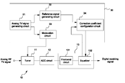
- FIG. 1 is a block diagram of an analog TV signal receiving circuit in accordance with an embodiment of the present invention.
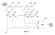
- FIG. 2 is a schematic diagram of the equalizer shown in FIG. 1 in accordance with an embodiment of the present invention.
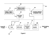
- FIG. 3 is a block diagram of an equalizer circuit coefficient defining apparatus in accordance with an embodiment of the present invention.
- FIG. 4 is a flow chart of an analog TV signal receiving method in accordance with an embodiment of the present invention.
- FIG. 5 is a flow chart of a method for defining coefficients of an equalizer in accordance with an embodiment of the present invention.
- FIG. 6 is a flow chart of details of generating an analog RF TV signal (Step 54 ) illustrated in FIG. 5 .
- FIG. 1 is a block diagram of an analog TV signal receiving circuit in accordance with an embodiment of the present invention.
- An analog TV signal receiving circuit 10 comprises a tuner 11 , an ADC circuit 12 , and a digital demodulator 13 .
- the tuner 11 performs frequency conversion on an analog RF TV signal received by the analog TV signal receiving circuit 10 to generate an analog frequency down conversion signal, which is optionally in various forms, but is mainly an intermediate (IF) signal.
- IF intermediate
- Such types of analog RF TV signals can conform to any type of analog TV specification, e.g., NTSC, PAL, SECAM, and the like.
- the ADC 12 performs analog-to-digital conversion to convert the analog frequency down conversion signal to a digital frequency down conversion signal.
- the digital demodulator 13 comprises a front-end circuit 131 and an equalizer 132 .
- the front-end circuit 131 generates a digital demodulated signal according to the digital frequency down conversion signal.
- the equalizer 132 generates a digital receiving signal according to the digital demodulated signal for performing subsequent signal processing, e.g., decoding.
- the equalizer 132 comprises a plurality of correction coefficients that are generated according to a predetermined rule, e.g., a least mean square (LMS) algorithm to be described below.
- LMS least mean square
- a main function of the equalizer 132 is to adjust signal distortion created in processing performed on a TV signal received by the analog TV signal receiving circuit 10 , e.g., the ringing effect or the ghost effect may occur during signal processing of the tuner 11 , the ADC 12 , and the front-end circuit 131 .
- FIG. 2 shows a schematic diagram of the equalizer 132 shown in FIG. 1 .
- the equalizer 132 comprises a finite impulse response (FIR) filter comprising n+1 taps P, where n is a positive integer, and each tap P corresponds to a weight coefficient—a correction coefficient generated according to the foregoing predetermined rule.
- each tap P has a multiplexer 1321 corresponding to a weight coefficient h(k), where k is between 0 and n.
- a delay component 1322 is coupled between every two adjacent taps P, and outputs of taps P are summed and outputted via an adder 1323 . Equalization is performed on the digital demodulated signal outputted by the front-end circuit 131 via the FIR filter in FIG. 2 to adjust the signal distortion.
- the analog TV signal receiving circuit 10 further comprises an equalizer coefficient defining apparatus 30 for defining correction coefficients of the equalizer 132 as shown in FIG. 3 .
- the equalizer coefficient defining apparatus 30 two identical simulation analog TV signals pass through two paths, of which a digital reference signal is outputted along one path and transmission (not including channel transmission) and reception of the analog TV signal are simulated along the other path, so as to output a simulation digital receiving signal.
- the simulation digital receiving signal is compared with the foregoing digital reference signal to accurately and specifically estimate an extent of the signal distortion created in the reception process of the analog TV signal received by the analog TV signal receiving circuit.
- the equalizer coefficient defining apparatus 30 comprises an analog TV signal generator 31 , a reference signal generator 32 , a modulator 33 , and a correction coefficient configuration circuit 34 .
- the analog TV signal generator 31 provides a simulation analog TV signal that is not limited to any particular type of analog TV specification.
- the simulation analog TV signal has a specific image pattern, and more specifically, has an image pattern to more easily to create image distortion. The pattern is readily apparent to a person having ordinary skill in the art, and details thereof shall not be described for brevity.
- the reference signal generator 32 being one of the foregoing two paths, generates the digital reference signal according to the simulation analog TV signal provided by the analog TV signal generator, e.g., the reference signal generator 32 is an ADC, which directly converts the simulation analog TV signal to a simulation digital TV signal regarded as the digital reference signal.
- the other path is formed by modulator 33 and the analog TV signal receiving circuit 10 .
- the modulator 33 modulates the simulation analog TV signal provided by the analog TV signal generator 31 to a simulation analog RF TV signal, aiming to simulate a transmission end for the analog TV signal.
- the analog TV signal receiving circuit 10 coupled to the modulator 33 receives the simulation analog RF TV signal that is in sequence processed by internal circuits (including the tuner 11 , the ADC 12 , the front-end circuit 131 , and the equalizer 132 , wherein a signal outputted from the front-end circuit 131 to the equalizer 132 is a simulation digital demodulated signal) to generate the foregoing simulation digital receiving signal, aiming to simulate a receiving end for the analog TV signal.
- the simulation digital receiving signal is a digital version of the simulation analog TV signal that is processed via modulation and demodulation.
- the extent of the signal distortion is estimated by comparing the simulation digital receiving signal with the foregoing digital reference signal (i.e., the directly-digitalized simulation analog TV signal).
- the equalizer coefficient configuration apparatus 30 in FIG. 3 mainly estimates the signal distortion created at the receiving end without consideration of the channel transmission effect.
- the correction coefficient configuration circuit 34 coupled to the reference signal generator 32 and the equalizer 132 respectively, defines the correction coefficients of the equalizer 132 according to the digital reference signal, the simulation digital receiving signal, and the abovementioned predetermined rule.
- the predetermined rule is the LMS algorithm.
- An approach for the correction coefficient configuration circuit 34 to define the correction coefficients of the equalizer 132 according to the LMS algorithm is further described below.
- the correction coefficient configuration circuit 34 performs synchronization on the digital reference signal and the simulation digital receiving signal to estimate a difference between the two signals.
- the simulation analog TV signal provided by the analog TV signal generating circuit 31 comprises a synchronization signal (e.g., a vertical synchronization (V-Sync) signal) and a horizontal synchronization (H-Sync) signal, which respectively represent start time points of each TV frame and each scan line, so that both of the digital reference signal and the simulation digital receiving signal comprise the synchronization signals.
- the correction coefficient configuration circuit 34 performs synchronization of the digital reference signal and the simulation digital receiving signal via the synchronization signals.
- the correction coefficient configuration circuit 34 calculates the correction coefficients of the equalizer 132 according to following Equation 1 and Equation 2.
- the index i is a positive integer.
- Equation 1 x i is an ith output signal (i.e., the simulation digital receiving signal) of the equalizer 132 , and d i is an ith output signal (i.e., the digital reference signal) of the reference signal generating circuit 32 , so that e i is the difference (i.e., a so-called difference signal) between the simulation digital receiving signal and the digital reference signal.
- x i ⁇ right arrow over (h) ⁇ i ⁇ right arrow over (r) ⁇ i in Equation 1 represents a calculation process of the equalizer 132 in FIG. 2 .
- ⁇ right arrow over (h) ⁇ i represents an ith weight coefficient (i.e., an correction coefficient) of each tap P, i.e., vectors h( 0 ) i , h( 1 ) i , . . . , h(n) i , that represent current values of the weight coefficient.
- ⁇ right arrow over (r) ⁇ i represents a current value (i.e., the simulation digital demodulated signal) temporarily stored in each delay component 1322 and the simulation digital demodulated signal currently inputted into the equalizer 132 , i.e., vectors formed by consecutive n+1 sampling values of the simulation digital demodulated signal. Therefore, x i outputted by the equalizer 132 is equal to a convolution of the two vectors ⁇ right arrow over (h) ⁇ i and ⁇ right arrow over (r) ⁇ i .
- Equation 2 the (i+1)th weight coefficient of each tap P of the equalizer 132 is calculated according to Equation 2 to be represented as vectors (h( 0 ) i+1 , h( 1 ) i+1 , . . . , h(n) i+1 ), meaning a next value of the weight coefficient (compared to the current value of the weight coefficient).
- ⁇ represents a coefficient adjustment value that is dynamically adjusted during the entire coefficient configuration process.
- the correction coefficient configuration circuit 34 distributes the new weight coefficient obtained according to Equation 2 to taps P of the equalizer 132 , and the equalizer coefficient configuration apparatus 30 iterates the foregoing operations according to the new weight coefficient until a converged weight coefficient is obtained.
- correction coefficient configuration circuit 34 determines
- the foregoing coefficient adjustment value ⁇ is defined as 0 to interrupt the LMS algorithm.
- FIG. 4 is a flow chart of a method for reducing signal distortion when an analog TV signal receiving circuit is receiving signals in accordance with an embodiment of the present invention. The method is applied to the analog TV signal receiving circuit 10 shown in FIG. 1 .
- an analog RF TV signal is received.
- an analog frequency down conversion signal is generated according to the analog RF TV signal.
- a digital frequency down conversion signal is generated according to the analog frequency down conversion signal.
- a digital demodulated signal is generated according to the digital frequency down conversion signal.
- a digital receiving signal is generated via an equalizer (e.g., the equalizer 132 as shown in FIG. 1 ) according to the digital demodulated signal.
- an equalizer e.g., the equalizer 132 as shown in FIG. 1
- the equalizer comprises a plurality of correction coefficients that are generated according to a predetermined rule, e.g., the LMS algorithm.
- Step 45 is to adjust signal distortion generated during Step 42 and Step 44 , e.g., a ringing effect and a ghost effect.
- FIG. 5 is a flow chart of a method for defining configuration coefficients of an equalizer in accordance with an embodiment of the present invention. The method is applied to the equalizer coefficient configuration apparatus 30 shown in FIG. 3 .
- an analog TV signal is provided. After the analog TV signal is provided, two types of processing take place.
- a digital reference signal is generated according to the analog TV signal.
- an analog RF TV signal is generated according to the analog TV signal.
- a digital receiving signal is generated via an analog TV signal receiving circuit (e.g., the analog TV signal receiving circuit 10 shown in FIG. 1 ). The generation of a digital receiving signal described in Step 54 can be seen in greater detail referring to FIG.
- Step 541 an analog frequency down conversion signal is generated according to the analog RF TV signal.
- Step 542 a digital frequency down conversion signal is generated according to the analog frequency down conversion signal.
- Step 543 a digital demodulated signal is generated according to the digital frequency down conversion signal.
- Step 544 according to the digital demodulated signal, the digital receiving signal is generated via an equalizer of the analog TV signal receiving circuit, e.g., the equalizer 132 of the analog TV signal receiving circuit 10 .
- the plurality of correction coefficients of the equalizer are defined according to a predetermined rule, the digital reference signal, and the digital receiving signal in Step 55 .
- Step 55 comprises synchronizing the digital reference signal and the digital receiving signal; calculating a difference between the digital reference signal and the digital receiving signal; and configuring next values of the correction coefficients according to current values of the correction coefficients, a coefficient adjustment value, the difference, and the digital demodulated signal.
- an analog TV signal receiving circuit comprises an equalizer to adjust signal distortion created during a reception process of an analog TV signal, and correction coefficients of the equalizer are defined via a configuration apparatus and associated method provided by the present invention, resulting in a reduction of the signal distortion during analog television signal reception.
Landscapes
- Engineering & Computer Science (AREA)
- Multimedia (AREA)
- Signal Processing (AREA)
- Cable Transmission Systems, Equalization Of Radio And Reduction Of Echo (AREA)
- Noise Elimination (AREA)
- Circuits Of Receivers In General (AREA)
Abstract
Description
e i =d i −x i, where x i ={right arrow over (h)} i
{right arrow over (h)} i+1 ={right arrow over (h)} i +μe i {right arrow over (r)} i; Equation 2:
The index i is a positive integer. In
Claims (18)
Applications Claiming Priority (3)
| Application Number | Priority Date | Filing Date | Title |
|---|---|---|---|
| TW100105196A | 2011-02-17 | ||
| TW100105196A TWI415459B (en) | 2011-02-17 | 2011-02-17 | Analog tv receiver and method and associated device and method for configuring equalizer coefficients |
| TW100105196 | 2011-02-22 |
Publications (2)
| Publication Number | Publication Date |
|---|---|
| US20120212674A1 US20120212674A1 (en) | 2012-08-23 |
| US8525932B2 true US8525932B2 (en) | 2013-09-03 |
Family
ID=46652434
Family Applications (1)
| Application Number | Title | Priority Date | Filing Date |
|---|---|---|---|
| US13/216,356 Expired - Fee Related US8525932B2 (en) | 2011-02-17 | 2011-08-24 | Analog TV signal receiving circuit for reducing signal distortion using equalizer configuring method |
Country Status (2)
| Country | Link |
|---|---|
| US (1) | US8525932B2 (en) |
| TW (1) | TWI415459B (en) |
Citations (3)
| Publication number | Priority date | Publication date | Assignee | Title |
|---|---|---|---|---|
| US20060050814A1 (en) * | 2004-09-03 | 2006-03-09 | Mediatek Inc. | Decoding apparatus and method of optical information reproducing system |
| US20060176948A1 (en) * | 2005-02-04 | 2006-08-10 | Dong-Hoon Lee | Decision-feedback channel equalizer usable with a digital receiver and method thereof |
| US20080232453A1 (en) * | 2007-03-22 | 2008-09-25 | Zoran Corporation | Combining least squares and least mean squares algorithms to determine equalizer tap values |
Family Cites Families (3)
| Publication number | Priority date | Publication date | Assignee | Title |
|---|---|---|---|---|
| US6285412B1 (en) * | 1997-07-23 | 2001-09-04 | Harris Corporation | Adaptive pre-equalization apparatus for correcting linear distortion of a non-ideal data transmission system |
| US7525600B2 (en) * | 2005-01-14 | 2009-04-28 | Broadcom Corporation | Single integrated high definition television (HDTV) chip for analog and digital reception |
| CN101147393B (en) * | 2005-03-24 | 2011-08-17 | 汤姆森特许公司 | Device and method for tuning radio frequency signal |
-
2011
- 2011-02-17 TW TW100105196A patent/TWI415459B/en not_active IP Right Cessation
- 2011-08-24 US US13/216,356 patent/US8525932B2/en not_active Expired - Fee Related
Patent Citations (3)
| Publication number | Priority date | Publication date | Assignee | Title |
|---|---|---|---|---|
| US20060050814A1 (en) * | 2004-09-03 | 2006-03-09 | Mediatek Inc. | Decoding apparatus and method of optical information reproducing system |
| US20060176948A1 (en) * | 2005-02-04 | 2006-08-10 | Dong-Hoon Lee | Decision-feedback channel equalizer usable with a digital receiver and method thereof |
| US20080232453A1 (en) * | 2007-03-22 | 2008-09-25 | Zoran Corporation | Combining least squares and least mean squares algorithms to determine equalizer tap values |
Also Published As
| Publication number | Publication date |
|---|---|
| US20120212674A1 (en) | 2012-08-23 |
| TW201236456A (en) | 2012-09-01 |
| TWI415459B (en) | 2013-11-11 |
Similar Documents
| Publication | Publication Date | Title |
|---|---|---|
| TW306112B (en) | ||
| JP3391761B2 (en) | Equalizer and method for equalizing digital signal | |
| US8208530B2 (en) | Apparatus and method for correcting IQ imbalance | |
| KR100954506B1 (en) | Matched Pulse Shaping Filters | |
| TW201312981A (en) | Timing recovery module and timing recovery method | |
| US7406132B2 (en) | Pre-equalizer, VSB transmission system using the same, and transmission method thereof | |
| KR100557122B1 (en) | A receiver for dtv signals subject to co-channel ntsc interference and method of operating therefor | |
| CN100463505C (en) | Method for suppressing co-channel interference signal and related filtering system and receiver | |
| US8525932B2 (en) | Analog TV signal receiving circuit for reducing signal distortion using equalizer configuring method | |
| JP4654067B2 (en) | Channel state evaluation method and channel state generation circuit in digital television receiver | |
| CN107026806B (en) | Receiving equipment, receiving method and program | |
| US7739320B2 (en) | Waveform equalizer, waveform equalization method, and integrated circuit | |
| KR20040038249A (en) | Equalizer for digital television receiver | |
| CN102647568B (en) | Method and circuit for reducing signal distortion of analog TV signal | |
| CA2447932A1 (en) | Equalizer for a single-carrier receiver and equalization method therefor | |
| JP4283689B2 (en) | Waveform equalizer | |
| JP2006166402A (en) | Waveform equalization apparatus, waveform equalization method, and integrated circuit | |
| US20100208135A1 (en) | Method for processing an analog television signal | |
| JP2004007577A (en) | Method and equalizer system equipped with comb filter for high definition television system | |
| Kim et al. | A new ghost cancellation system for Korean GCR | |
| JP3226228B2 (en) | Waveform equalization circuit | |
| KR20040006448A (en) | Method of channel estimation and equalizer coefficient initialization in digital transmit-receive system | |
| KR101034455B1 (en) | Co-channel repeater and method for removing feedback signal | |
| JP3011422B2 (en) | Waveform equalizer and waveform equalization method | |
| KR20120135630A (en) | Device and method for receiver of hybrid signal |
Legal Events
| Date | Code | Title | Description |
|---|---|---|---|
| AS | Assignment |
Owner name: MSTAR SEMICONDUCTOR, INC., TAIWAN Free format text: ASSIGNMENT OF ASSIGNORS INTEREST;ASSIGNORS:LAN, CHING FU;YANG, WEN CHIEH;LAI, YI HSUAN;AND OTHERS;SIGNING DATES FROM 20110228 TO 20110603;REEL/FRAME:026797/0763 |
|
| FEPP | Fee payment procedure |
Free format text: PAYOR NUMBER ASSIGNED (ORIGINAL EVENT CODE: ASPN); ENTITY STATUS OF PATENT OWNER: LARGE ENTITY |
|
| STCF | Information on status: patent grant |
Free format text: PATENTED CASE |
|
| FPAY | Fee payment |
Year of fee payment: 4 |
|
| AS | Assignment |
Owner name: MEDIATEK INC., TAIWAN Free format text: MERGER;ASSIGNOR:MSTAR SEMICONDUCTOR, INC.;REEL/FRAME:052931/0468 Effective date: 20190115 |
|
| AS | Assignment |
Owner name: XUESHAN TECHNOLOGIES INC., CANADA Free format text: ASSIGNMENT OF ASSIGNORS INTEREST;ASSIGNOR:MEDIATEK INC.;REEL/FRAME:055486/0870 Effective date: 20201223 |
|
| MAFP | Maintenance fee payment |
Free format text: PAYMENT OF MAINTENANCE FEE, 8TH YEAR, LARGE ENTITY (ORIGINAL EVENT CODE: M1552); ENTITY STATUS OF PATENT OWNER: LARGE ENTITY Year of fee payment: 8 |
|
| FEPP | Fee payment procedure |
Free format text: MAINTENANCE FEE REMINDER MAILED (ORIGINAL EVENT CODE: REM.); ENTITY STATUS OF PATENT OWNER: LARGE ENTITY |
|
| LAPS | Lapse for failure to pay maintenance fees |
Free format text: PATENT EXPIRED FOR FAILURE TO PAY MAINTENANCE FEES (ORIGINAL EVENT CODE: EXP.); ENTITY STATUS OF PATENT OWNER: LARGE ENTITY |
|
| STCH | Information on status: patent discontinuation |
Free format text: PATENT EXPIRED DUE TO NONPAYMENT OF MAINTENANCE FEES UNDER 37 CFR 1.362 |
|
| FP | Lapsed due to failure to pay maintenance fee |
Effective date: 20250903 |