US8520163B2 - Light source assembly and LCD - Google Patents
Light source assembly and LCD Download PDFInfo
- Publication number
- US8520163B2 US8520163B2 US13/318,350 US201113318350A US8520163B2 US 8520163 B2 US8520163 B2 US 8520163B2 US 201113318350 A US201113318350 A US 201113318350A US 8520163 B2 US8520163 B2 US 8520163B2
- Authority
- US
- United States
- Prior art keywords
- hole
- insulative
- disposed
- nesting
- insulative insert
- Prior art date
- Legal status (The legal status is an assumption and is not a legal conclusion. Google has not performed a legal analysis and makes no representation as to the accuracy of the status listed.)
- Expired - Fee Related, expires
Links
Images


Classifications
-
- G—PHYSICS
- G02—OPTICS
- G02F—OPTICAL DEVICES OR ARRANGEMENTS FOR THE CONTROL OF LIGHT BY MODIFICATION OF THE OPTICAL PROPERTIES OF THE MEDIA OF THE ELEMENTS INVOLVED THEREIN; NON-LINEAR OPTICS; FREQUENCY-CHANGING OF LIGHT; OPTICAL LOGIC ELEMENTS; OPTICAL ANALOGUE/DIGITAL CONVERTERS
- G02F1/00—Devices or arrangements for the control of the intensity, colour, phase, polarisation or direction of light arriving from an independent light source, e.g. switching, gating or modulating; Non-linear optics
- G02F1/01—Devices or arrangements for the control of the intensity, colour, phase, polarisation or direction of light arriving from an independent light source, e.g. switching, gating or modulating; Non-linear optics for the control of the intensity, phase, polarisation or colour
- G02F1/13—Devices or arrangements for the control of the intensity, colour, phase, polarisation or direction of light arriving from an independent light source, e.g. switching, gating or modulating; Non-linear optics for the control of the intensity, phase, polarisation or colour based on liquid crystals, e.g. single liquid crystal display cells
- G02F1/133—Constructional arrangements; Operation of liquid crystal cells; Circuit arrangements
- G02F1/1333—Constructional arrangements; Manufacturing methods
- G02F1/1335—Structural association of cells with optical devices, e.g. polarisers or reflectors
- G02F1/1336—Illuminating devices
- G02F1/133602—Direct backlight
- G02F1/133604—Direct backlight with lamps
Definitions
- the present invention generally relates to a light source assembly, and more particularly, to a light source assembly for a liquid crystal display (LCD) and the LCD.
- LCD liquid crystal display
- LCDs liquid crystal displays
- PDAs personal digital assistants
- the light source assembly comprises a light tube 11 , a lead 12 and a connector 13 .
- the light tube 11 comprises a tube body 111 and a pin 112 disposed at an end of the tube body 111 .
- the lead 12 has an end welded onto the pin 112 and the other end connected to the connector 13 .
- the connector 13 is further connected to an external connector 15 on a circuit board 14 .
- glass of the tube body 111 tends to be thermally damaged due to a high temperature of the soldering iron. This may lead to gas leakage from the tube body 111 to cause failure of the light tube 11 . In this case, the damaged light tube 11 must be replaced with a new one and the welding process must be repeated, thus increasing the cost.
- the primary objective of the present invention is to provide a light source assembly and a liquid crystal display (LCD), which can prevent a light tube from being damaged when a lead is welded so as to save the cost.
- LCD liquid crystal display
- the present invention provides a light source assembly, which comprises a light tube, a conductive nesting element, a first insulative insert, a second insulative insert and a lead.
- the light tube comprises a tube body and a pin, wherein the pin is disposed at an end of the tube body.
- the conductive nesting element comprises a nesting body and a flap, wherein the nesting body is fitted over and fixed to an end of the tube body and is electrically connected to the pin, and the flap is disposed on the nesting body and extends in a direction lateral to the light tube.
- the first insulative insert is formed with a first through-hole, a second through-hole and a blind hole, wherein the first through-hole connects two opposite sides of the first insulative insert, the second through-hole connects to the first through-hole and connects the two opposite sides of the first insulative insert, the blind hole connects to the first through-hole and connects one of the sides of the first insulative insert that is away from the light tube, the first through-hole is disposed to allow the nesting body to pass through the first insulative insert, the second through-hole is disposed to allow the flap to pass through the first insulative insert, and the blind hole is disposed to allow the flap to be disposed and supported in the blind hole from a side away from the light tube.
- the second insulative insert is fixed on the first insulative insert, wherein the second insulative insert comprises an insulative body and a conductive elastic piece disposed inside the insulative body, both ends of the conductive elastic piece are exposed from two opposite sides of the insulative body, and one end of the conductive elastic piece abuts against the flap located in the blind hole.
- the lead has an end electrically connected to the other end of the conductive elastic piece.
- the second insulative insert further comprises an upright post disposed on a side surface of the insulative body near the light tube, and the upright post is inserted and fixed into the second through-hole.
- the nesting body comprises a first bushing and a second bushing, the first bushing is fitted over an end of the tube body, the second bushing is fitted over the pin and is press-fitted to the pin, and the flap is disposed on the first bushing.
- the present invention further provides a light source assembly, which comprises a light tube, a conductive nesting element, a first insulative insert and a second insulative insert.
- the light tube comprises a tube body and a pin, wherein the pin is disposed at an end of the tube body.
- the conductive nesting element comprises a nesting body and a flap, wherein the nesting body is fitted over and fixed to an end of the tube body and is electrically connected to the pin, and the flap is disposed on the nesting body and extends in a direction lateral to the light tube.
- the first insulative insert is formed with a first through-hole and a blind hole, wherein the first through-hole connects two opposite sides of the first insulative insert to allow the nesting body to be inserted through the first through-hole, and the blind hole connects to the first through-hole and connects one of the sides of the first insulative insert that is away from the light tube to allow the flap to be disposed and supported in the blind hole from a side away from the light tube.
- the second insulative insert is fixed on the first insulative insert, wherein the second insulative insert comprises an insulative body and a conductive elastic piece disposed inside the insulative body, both ends of the conductive elastic piece are exposed from two opposite sides of the insulative body, and one end of the conductive elastic piece abuts against the flap located in the blind hole.
- the first insulative insert is further formed with a second through-hole, the second through-hole connects to the first through-hole and connects the two opposite sides of the first insulative insert, the first through-hole is disposed to allow the nesting body to pass through the first insulative insert, and the second through-hole is disposed to allow the flap to pass through the first insulative insert.
- the second insulative insert further comprises an upright post disposed on a side surface of the insulative body near the light tube, and the upright post is inserted and fixed into the second through-hole.
- the upright post is interference-fitted into the second through-hole.
- the flaps are disposed at two opposite sides of the nesting body respectively, and the second through-holes and the blind holes are arranged in the form of a cross with the first through-hole as a center.
- the flaps, the second through-holes and the blind holes have a rectangular section in a direction perpendicular to the tube body.
- the light source assembly further comprises a lead, which has an end electrically connected to the other end of the conductive elastic piece.
- the light source assembly further comprises a connector, which is electrically connected to the other end of the lead.
- the nesting body comprises a first bushing and a second bushing, the first bushing is fitted over an end of the tube body, and the second bushing is fitted over and press-fitted to the pin.
- the present invention further provides an LCD comprising a light source assembly, wherein the light source assembly further comprises a light tube, a conductive nesting element, a first insulative insert and a second insulative insert.
- the light tube comprises a tube body and a pin, wherein the pin is disposed at an end of the tube body.
- the conductive nesting element comprises a nesting body and a flap, wherein the nesting body is fitted over and fixed to an end of the tube body and is electrically connected to the pin, and the flap is disposed on the nesting body and extends in a direction lateral to the light tube.
- the first insulative insert is formed with a first through-hole and a blind hole, wherein the first through-hole connects two opposite sides of the first insulative insert to allow the nesting body to be inserted through the first through-hole, and the blind hole connects to the first through-hole and connects one of the sides of the first insulative insert that is away from the light tube to allow the flap to be disposed and supported in the blind hole from a side away from the light tube.
- the second insulative insert is fixed on the first insulative insert, wherein the second insulative insert comprises an insulative body and a conductive elastic piece disposed inside the insulative body, both ends of the conductive elastic piece are exposed from two opposite sides of the insulative body, and one end of the conductive elastic piece abuts against the flap located in the blind hole.
- the first insulative insert is further formed with a second through-hole, the second through-hole connects to the first through-hole and connects the two opposite sides of the first insulative insert, the first through-hole is disposed to allow the nesting body to pass through the first insulative insert, and the second through-hole is disposed to allow the flap to pass through the first insulative insert.
- the second insulative insert further comprises an upright post disposed on a side surface of the insulative body near the light tube, and the upright post is inserted and fixed into the second through-hole.
- the upright post is interference-fitted into the second through-hole.
- the light source assembly further comprises a lead, which has an end electrically connected to the other end of the conductive elastic piece.
- the light source assembly further comprises a connector, which is electrically connected to the other end of the lead.
- the nesting body comprises a first bushing and a second bushing, the first bushing is fitted over an end of the tube body, and the second bushing is fitted over and press-fitted to the pin.
- the present invention has the following benefits: as compared to the prior art, the light source assembly and the LCD of the present invention can prevent damage to the light tube when the lead is welded onto the pin of the light tube, so they can save the cost.
- FIG. 1 is a schematic perspective view of a light source assembly for an LCD in the prior art
- FIG. 2 is a schematic perspective view of a light source assembly according to a first embodiment of the present invention in an exploded status
- FIG. 3 is a schematic perspective view of a first insulative insert in the light source assembly of FIG. 2 ;
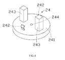
- FIG. 4 is a schematic perspective view of a second insulative insert in the light source assembly of FIG. 2 ;
- FIG. 5 is a cross-sectional view of the light source assembly of FIG. 2 in an assembled status.
- a light source assembly of the present invention mainly comprises a light tube 21 , a conductive nesting element 22 , a first insulative insert 23 , a second insulative insert 24 , leads 25 and a connector 26 .
- the light tube 21 comprises a tube body 211 and a pin 212 , and the pin 212 is disposed at an end of the tube body 211 .
- the light tube 21 may be a cold cathode fluorescence lamp (CCFL) tube well known in the art.
- CCFL cold cathode fluorescence lamp
- the conductive nesting element 22 comprises a nesting body 221 and flaps 222 .
- the nesting body 221 is fitted over and fixed to an end of the tube body 211 and is electrically connected to the pin 212 .
- the nesting body 221 comprises a first bushing 2211 and a second bushing 2212 , the first bushing 2211 is fitted over an end of the tube body 211 , and the second bushing 2212 is fitted over and press-fitted to the pin 212 .
- the nesting body 221 may also be fixed to the end of the tube body 211 and be electrically connected to the pin 212 in other ways; e.g., the nesting body 221 may be glued to the end of the tube body 211 and be electrically connected to the pin 212 by making a contact with the pin 212 .
- the flaps 222 are disposed on the nesting body 221 and extend in a direction lateral to the light tube 21 .
- the flaps 222 are integrally formed with the nesting body 221 .
- each of the flaps 222 is formed by cutting a strip-like area on a side wall of the first bushing 2211 and then bending the strip-like area in the direction lateral to the light tube 21 .
- the flaps 222 may also be formed and disposed on the nesting body 221 in other ways; e.g., the flaps 222 may be formed as separate conductive components in an appropriate way, and then fixed to the nesting body 221 through welding or in other ways.
- the flaps 222 there are two flaps 222 , which are formed at two sides of the nesting body 221 respectively. Meanwhile, the flaps 222 have a rectangular cross-section in a direction perpendicular to the tube body 211 . In other embodiments, there may also be one or more than two flaps 222 depending on practical requirements, and the flaps 222 may also be designed to have other shapes depending on practical requirements.
- the first insulative insert 23 is formed with a first through-hole 231 , second through-holes 232 and blind holes 233 .
- the first through-hole 231 connects two opposite sides of the first insulative insert 23 (an upper side and a lower side of the first insulative insert 23 as shown in FIG. 3 ) to allow the nesting body 221 to be inserted through the first through-hole 231 .
- the first through-hole 231 further allows the nesting body 221 to pass through the first insulative insert 23 .
- Each of the second through-holes 232 connects to the first through-hole 231 and connects the two opposite sides of the first insulative insert 23 (the upper side and the lower side of the first insulative insert 23 as shown in FIG.
- Each of the blind holes 233 connects to the first through-hole 231 and connects one of the sides of the first insulative insert 23 that is away from the light tube 21 (the upper side of the first insulative insert 23 as shown in FIG. 3 ) to allow the flaps 222 to be disposed and supported in the blind hole 233 from the side away from the light tube 21 .
- the flaps 222 and the blind holes 233 are closely fitted with each other.
- the numbers of the second through-holes 232 and the blind holes 233 are also two respectively; and the second through-holes 232 and the blind holes 233 are arranged in the form of a cross with the first through-hole 231 as a center. Meanwhile, the second through-holes 232 and the blind holes 233 also have a rectangular cross-section in the direction perpendicular to the tube body 211 . In other embodiments, the numbers and the shapes of the second through-holes 232 and the blind holes 233 may vary depending on the number and the shape of the flaps 222 .
- the second insulative insert 24 comprises an insulative body 241 , conductive elastic pieces 242 and upright posts 243 .
- the conductive elastic pieces 242 are disposed inside the insulative body 241 , and both ends of each of the conductive elastic pieces 242 are exposed from two opposite sides of the insulative body 241 .
- the conductive elastic pieces 242 may be disposed inside the insulative body 241 through injection moulding.
- the upright posts 243 are disposed on a side surface of the insulative body 241 near the light tube 21 , and each of the upright posts 243 is inserted and fixed into one of the second through-holes 232 so that the second insulative insert 24 is fixed to the first insulative insert 23 .
- the upright posts 243 may be integrally formed with the insulative body 241 through injection moulding.
- the second insulative insert 24 is fixed to the first insulative insert 23 , one end of each of the conductive elastic pieces 242 abuts against one of the flaps 222 located in the blind holes 233 .
- the upright posts 243 are interference-fitted into the second through-holes 232 .
- the second insulative insert 24 may also be fixed to the first insulative insert 23 in other ways, for example, through gluing, snap-fitting or screwing.
- each of the conductive elastic pieces 242 preferably has a bent structure at an end thereof to elastically abut against one of the flaps 222 .
- the numbers of the upright posts 243 and the conductive elastic pieces 242 are also two respectively; meanwhile, the upright posts 243 also have a rectangular cross-section in the direction perpendicular to the tube body 211 .
- the numbers of the upright posts 243 and the conductive elastic pieces 242 and the shape of the upright posts 243 may vary depending on the numbers and shapes of the second through-holes 232 and the flaps 222 .
- the side surface of the insulative body 241 near the light tube 21 is further formed with a blind hole 244 , which is adapted to receive the pin 212 of the light tube 21 and the second bushing 2212 of the conductive nesting element 22 . This can shorten the length of the first insulative insert 23 .
- each of the leads 25 is electrically connected to the other end of one of the conductive elastic pieces 242 through welding or in other ways.
- the connector 26 is electrically connected to the other end of each of the leads 25 through welding or in other ways.
- the connector 26 is further connected to an external connector 28 disposed on a circuit board 27 .
- the nesting body 221 of the conductive nesting element 22 is fitted over and fixed to an end of the tube body 211 and is electrically connected to the pin 212 . Then, the nesting body 221 and the flaps 222 of the conductive nesting element 22 are inserted through the first insulative insert 23 via the first through-hole 231 and the second through-holes 232 respectively. Next, the conductive nesting element 22 is rotated by 90°, and the flaps 222 are disposed and supported in the blind holes 233 from a side of the first insulative insert 23 away from the light tube 21 .
- each of the leads 25 is electrically connected to the other end of one of the conductive elastic pieces 242 , and the other end of each of the leads 25 is electrically connected to the connector 26 .
- the second through-holes 232 and the upright posts 243 may also be omitted.
- the first insulative insert 23 is fitted over the tube body 211 via the first through-hole 231 , and then the nesting body 221 of the conductive nesting element 22 is fitted over and fixed to an end of the tube body 211 .
- the nesting body 221 is inserted through the first through-hole 231 from a side of the first insulative insert 23 away from the light tube 21 , and the flaps 222 are disposed and supported in the blind holes 233 .
- the insulative body 241 of the second insulative insert 24 is fixed to the first insulative insert 23 in other ways (e.g., through gluing, snap-fitting or screwing), with one end of each of the conductive elastic pieces 242 abutting against one of the flaps 222 located in the blind holes 233 .
- the present invention further provides a liquid crystal display (LCD), which comprises the light source assembly described in the aforesaid embodiment.
- LCD liquid crystal display
- the light source assembly and the LCD of the present invention can save the cost.
Landscapes
- Physics & Mathematics (AREA)
- Nonlinear Science (AREA)
- Mathematical Physics (AREA)
- Chemical & Material Sciences (AREA)
- Crystallography & Structural Chemistry (AREA)
- General Physics & Mathematics (AREA)
- Optics & Photonics (AREA)
- Fastening Of Light Sources Or Lamp Holders (AREA)
- Planar Illumination Modules (AREA)
Abstract
Description
Claims (20)
Applications Claiming Priority (4)
| Application Number | Priority Date | Filing Date | Title |
|---|---|---|---|
| CN 201110040771 CN102141221B (en) | 2011-02-18 | 2011-02-18 | Light source assembly |
| CN201110040771 | 2011-02-18 | ||
| CN201110040771.X | 2011-02-18 | ||
| PCT/CN2011/074735 WO2012109827A1 (en) | 2011-02-18 | 2011-05-26 | Light source assembly and liquid crystal display |
Publications (2)
| Publication Number | Publication Date |
|---|---|
| US20120212688A1 US20120212688A1 (en) | 2012-08-23 |
| US8520163B2 true US8520163B2 (en) | 2013-08-27 |
Family
ID=46652440
Family Applications (1)
| Application Number | Title | Priority Date | Filing Date |
|---|---|---|---|
| US13/318,350 Expired - Fee Related US8520163B2 (en) | 2011-02-18 | 2011-05-26 | Light source assembly and LCD |
Country Status (1)
| Country | Link |
|---|---|
| US (1) | US8520163B2 (en) |
Citations (1)
| Publication number | Priority date | Publication date | Assignee | Title |
|---|---|---|---|---|
| US20020093815A1 (en) * | 2001-01-10 | 2002-07-18 | Yang-Wei Ou | Light-projector |
-
2011
- 2011-05-26 US US13/318,350 patent/US8520163B2/en not_active Expired - Fee Related
Patent Citations (1)
| Publication number | Priority date | Publication date | Assignee | Title |
|---|---|---|---|---|
| US20020093815A1 (en) * | 2001-01-10 | 2002-07-18 | Yang-Wei Ou | Light-projector |
Also Published As
| Publication number | Publication date |
|---|---|
| US20120212688A1 (en) | 2012-08-23 |
Similar Documents
| Publication | Publication Date | Title |
|---|---|---|
| US8773617B2 (en) | Liquid crystal display and LED module thereof | |
| US8251724B2 (en) | Lamp socket and display device having the same | |
| CN104345496B (en) | Flexure type display device | |
| US7926965B2 (en) | Lamp socket, backlight assembly and display device having the same | |
| US20100165231A1 (en) | Backlight module and display module | |
| US7880388B2 (en) | External electrode fluorescent lamp having conductive layer and backlight module utilizing same | |
| US8520163B2 (en) | Light source assembly and LCD | |
| CN101280908B (en) | Lamp tube fixing device | |
| US20130070166A1 (en) | Lighting device, display device and television device | |
| US20130010499A1 (en) | Backlight module and a backlight device | |
| KR20090102141A (en) | Backlight assembly and liquid crystal display comprising the same | |
| US20070030701A1 (en) | Backlight module with elastic connector clips fixing light source and liquid crystal display having same field of the invention | |
| CN101377590B (en) | Backlight module and its application | |
| US7999882B2 (en) | Liquid crystal module | |
| US7726867B2 (en) | Backlight module with conductive mechanisms therein for providing power to lamps thereof | |
| EP2226906A1 (en) | Relay connecter, assembling structure of relay connector and chassis, assembling structure of relay connector and power supply, assembling structure of discharge tube and power supply to relay connector, illuminator for display device, display device, and television receiver | |
| US20100026924A1 (en) | Light supplying unit and display device using the same | |
| US20100118517A1 (en) | Backlight module having replaceable lamp module | |
| KR200414749Y1 (en) | Lamp connection structure of backlight unit | |
| CN205157932U (en) | Light-emitting lamp strip structure and light-emitting unit using same | |
| US20110019127A1 (en) | Backlight assembly and display device having the same | |
| US20090135584A1 (en) | Light emitting module | |
| US7717606B2 (en) | Cables fixing apparatus for backlight module | |
| US20090059114A1 (en) | Backlight Module and Liquid Crystal Display Incorporating Same | |
| CN102141221A (en) | Light source assembly |
Legal Events
| Date | Code | Title | Description |
|---|---|---|---|
| AS | Assignment |
Owner name: SHENZHEN CHINA STAR OPTOELECTRONICS TECHNOLOGY CO. Free format text: ASSIGNMENT OF ASSIGNORS INTEREST;ASSIGNOR:YU, GANG;REEL/FRAME:027151/0333 Effective date: 20110824 |
|
| STCF | Information on status: patent grant |
Free format text: PATENTED CASE |
|
| FEPP | Fee payment procedure |
Free format text: PAYOR NUMBER ASSIGNED (ORIGINAL EVENT CODE: ASPN); ENTITY STATUS OF PATENT OWNER: LARGE ENTITY |
|
| FPAY | Fee payment |
Year of fee payment: 4 |
|
| MAFP | Maintenance fee payment |
Free format text: PAYMENT OF MAINTENANCE FEE, 8TH YEAR, LARGE ENTITY (ORIGINAL EVENT CODE: M1552); ENTITY STATUS OF PATENT OWNER: LARGE ENTITY Year of fee payment: 8 |
|
| FEPP | Fee payment procedure |
Free format text: MAINTENANCE FEE REMINDER MAILED (ORIGINAL EVENT CODE: REM.); ENTITY STATUS OF PATENT OWNER: LARGE ENTITY |
|
| LAPS | Lapse for failure to pay maintenance fees |
Free format text: PATENT EXPIRED FOR FAILURE TO PAY MAINTENANCE FEES (ORIGINAL EVENT CODE: EXP.); ENTITY STATUS OF PATENT OWNER: LARGE ENTITY |
|
| STCH | Information on status: patent discontinuation |
Free format text: PATENT EXPIRED DUE TO NONPAYMENT OF MAINTENANCE FEES UNDER 37 CFR 1.362 |
|
| FP | Lapsed due to failure to pay maintenance fee |
Effective date: 20250827 |