US8519515B2 - TSV structure and method for forming the same - Google Patents
TSV structure and method for forming the same Download PDFInfo
- Publication number
- US8519515B2 US8519515B2 US13/085,488 US201113085488A US8519515B2 US 8519515 B2 US8519515 B2 US 8519515B2 US 201113085488 A US201113085488 A US 201113085488A US 8519515 B2 US8519515 B2 US 8519515B2
- Authority
- US
- United States
- Prior art keywords
- conductive
- ring
- layer
- extension part
- core
- Prior art date
- Legal status (The legal status is an assumption and is not a legal conclusion. Google has not performed a legal analysis and makes no representation as to the accuracy of the status listed.)
- Active, expires
Links
Images


Classifications
-
- H10W20/20—
-
- H10W20/023—
-
- H10W20/2125—
-
- H10W20/2128—
-
- H10W20/217—
-
- H10W72/0198—
-
- H10W90/00—
-
- H10W90/297—
Definitions
- the present invention generally relates to a TSV (through-silicon via) structure and the method for forming the TSV structure.
- the present invention is directed to a through-silicon via with a double-ring structure in order to reduce the adverse electric coupling effect between the conductive substrate in the wafer and the conductive material in the through-silicon via structure.
- the through-silicon via technique is a quite novel semiconductor technique.
- the through-silicon via technique mainly resides in solving the problem of the electrical interconnection of chips and belongs to a new 3D packing field.
- the hot through-silicon via technique creates products which better meet the market trends of “light, thin, short and small” by the 3D stacking through the through-silicon via, to provide the micro electronic mechanic system (MEMS), the photoelectronics and electronic elements with packing techniques of wafer-level package.
- MEMS micro electronic mechanic system
- the through-silicon via technique drills holes in the wafer by etching or by laser then fills the holes with conductive materials, such as copper, polysilicon or tungsten to form vias, i.e. conductive channels connecting inner regions and outer regions.
- conductive materials such as copper, polysilicon or tungsten
- the wafer or the dice is thinned to be stacked or bonded together to be a 3D stack IC.
- the wire bonding procedure may be omitted.
- etching or laser to form conductive vias not only omits the wire bonding but also shrinks the occupied area on the circuit board and the volume for packing.
- the inner connection distance of the package by the through-silicon via technique i.e. the thickness of the thinned wafer or the dice
- the 3D stack IC has much shorter inner connection distance, so the 3D stack IC performs better in many ways, such as smaller electrical resistance, faster transmission, first noise and better performance.
- the advantages of the shorter inner connection distance of the through-silicon via technique are much more outstanding.
- the package size of the 3D stack IC equals to the size of the dice, so the through-silicon via technique is more valuable in the portable electronic devices.
- the through-silicon via technique may divided into two types, namely the via first or the via last.
- the via first process further includes two variations, called before CMOS and after CMOS.
- CMOS complementary metal-oxide-semiconductor
- the via-first-before-CMOS process through-silicon holes are formed on the silicon wafer and filled with a conductive material before the formation of the CMOS.
- the selection of the conductive material is basically focused on those which can survive after high temperatures, such as poly silicon, rather than the better copper because copper tends to form pumping and is unable to keep a low electrical resistance after being subject to thermal processes over and over again.
- the via-first-before-CMOS process is more compatible with the conventional CMOS process.
- the conductive material must bear high temperatures.
- the formation of the via and the filling of the conductive metal are done after the completion of the CMOS process.
- the current choice of the conductive metal is copper, which is much better than poly silicon in conductivity concern. Because the filling of copper may fail and some voids are formed due to the formation of void, tungsten gradually becomes an alternative choice. To be viewed as a whole, the filling of copper is particularly difficult and there is possible contamination of copper because the CMOS is completed, which makes it less compatible with the conventional CMOS process.
- the present invention proposes a novel TSV (through-silicon via) structure and the method for forming the TSV structure.
- the through-silicon via structure of the present invention has a specially designed composite ring structure in order to reduce or to eliminate the adverse electric coupling between the conductive substrate in the wafer and the conductive material in the through-silicon via structure.
- the present invention in a first aspect proposes a novel TSV structure.
- the TSV structure of the present invention includes a wafer, a through via, a conductive layer, a through via dielectric ring, a first conductive ring or a first substrate ring and a first dielectric ring.
- the wafer includes a first side and a second side.
- the through via is for use in connecting the first side and the second side of the wafer.
- the conductive layer fills up the through via and the through via dielectric ring surrounds and directly contacts the conductive layer.
- the first conductive ring or the first substrate ring surrounds and directly contacts the through via dielectric ring.
- the first dielectric ring surrounds and directly contacts the first conductive ring and is surrounded by the wafer.
- the present invention in a second aspect proposes a method for forming a through-silicon via structure.
- a wafer is provided.
- the wafer includes a substrate, a first side and a second side.
- a composite annular structure is formed in the wafer.
- the composite annular structure includes a core substrate column, a through via dielectric ring, a first substrate ring, and a first dielectric ring.
- the through via dielectric ring includes a dielectric material, surrounds and directly contacts the core substrate column.
- the first substrate ring surrounds and directly contacts the through via dielectric ring.
- the first dielectric ring surrounds and directly contacts the first substrate ring and is surrounded by the wafer.
- the wafer is thinned from the second side to expose the composite annular structure.
- a second dielectric layer is formed to cover the second side and to expose the composite annular structure.
- the substrate in the core substrate column is completely removed to form a through via which connects the first side and the second side.
- the through via is filled up with a core conductive layer to obtain the through-silicon via structure.
- the first substrate ring may be completely removed to form a first hollow ring before the first hollow ring is filled up with a first conductive material so that the first hollow ring becomes a first conductive ring.
- a semiconductor procedure may be carried out after the through-silicon via structure is obtained.
- a semiconductor procedure may be carried out before the through-silicon via structure is obtained.
- a multi-layer metal structure may be formed to be disposed on the first side and includes a first layer, a second layer and a third layer. A first conductive ring first extension part is composed of the first layer.
- a third conductive ring third extension part is composed of the third layer.
- a conductive layer extension part is composed of the second layer.
- the first conductive ring first extension part and the third conductive ring third extension part together sandwich the conductive layer extension part to shield the adverse interaction between the wafer and the conductive layer extension part.
- the conductive layer extension part may further have a serpent-like structure.
- FIGS. 1-6 illustrate the method for forming a through-silicon via structure of the present invention.
- FIGS. 7-10C and 12 illustrate the through-silicon via structure of the present invention.
- FIG. 11 illustrate to reduce or to block the adverse electrical coupling effect between the conductive substrate in the wafer and the core conductive material in the through-silicon via structure.
- the present invention in a first place provides a novel method for forming a TSV structure.
- the method of the present invention in particular forms a composite ring structure in order to reduce or to eliminate the adverse electric coupling between the conductive substrate in the wafer and the conductive material in the through-silicon via structure.
- FIGS. 1-10 illustrate the method for forming a through-silicon via structure of the present invention.
- a wafer 103 is provided.
- the wafer 103 is for use in forming a through-silicon via structure and includes a semiconductor substrate 103 .
- the wafer 103 also includes a first side 101 and a second side 102 which is opposite to the first side 101 .
- the first side 101 may be a front side of a semiconductor substrate for the preparation of various semiconductor elements and metal interconnection.
- the second side 102 may be a bottom side of a semiconductor substrate.
- the semiconductor substrate 103 may be Si.
- a composite annular structure 110 is formed in the wafer 103 .
- the composite annular structure 110 includes at least a core substrate column 111 , a through via dielectric ring 112 , a first substrate ring 113 , and a first dielectric ring 114 .
- the through via dielectric ring 112 includes a dielectric material, surrounds and directly contacts the core substrate column 111 .
- the first substrate ring 113 is located outside of the through via dielectric ring 112 so it surrounds and directly contacts the through via dielectric ring 112 .
- the first dielectric ring 114 is located outside of the first substrate ring 113 so it surrounds and directly contacts the first substrate ring 113 and it is at the same time surrounded by the semiconductor substrate 103 in the wafer.
- the composite annular structure 110 may be formed along with the formation of the shallow trench isolation (not shown). For example, lithographic and etching steps may be used to form recesses (not shown) in the wafer 103 to respectively define the through via dielectric ring 112 , the first dielectric ring 114 in the composite annular structure 110 and the shallow trench (not shown).
- the size of the openings on the reticle and etching recipes may be used to control the depth of the recesses and the shallow trenches. Preferably, the depth of the recesses should be deeper than that of the shallow trenches.
- a dielectric material such as silicon oxide, may be used to fill the recesses and the shallow trenches, followed by planarization to respectively obtain the through via dielectric ring 112 , the first dielectric ring 114 in the composite annular structure 110 and the shallow trench (not shown).
- the ring thickness of the through via dielectric ring 112 and the first dielectric ring 114 in the composite annular structure 110 may be 2 ⁇ m-3 ⁇ m.
- the semiconductor procedure may be any suitable semiconductor procedure.
- a semiconductor element 120 is accordingly formed on the first side 101 after this semiconductor procedure, and an interlayer dielectric layer 124 is formed on the semiconductor element 120 to cover the semiconductor element 120 as well as an interconnection structure 125 disposed on the interlayer dielectric layer 124 and electrically connected to the semiconductor element 120 .
- the optional semiconductor procedure may be carried out before or after the completion of the expected TSV structure.
- FIG. 2 illustrates the optional semiconductor procedure is carried out before the completion of the expected TSV structure.
- the semiconductor element 120 may include a gate 123 , and a source 121 and a drain 122 disposed adjacent to the gate 123 .
- the interconnection structure 125 penetrates the interlayer dielectric layer 124 and is electrically connected to the corresponding source 121 , the drain 122 and the gate 123 on the first side 101 through some contact plugs 126 .
- the interlayer dielectric layer 124 may include one or more dielectric material, such as silicon oxide, silicon nitride, low-k dielectric material, silicon oxynitride, silicon carbide or the combination thereof.
- the interconnection structure 125 may be a copper damascene conductive structure made by damascene steps and including a barrier layer, a seed layer and a copper layer.
- the contact plugs 126 usually include W, and Ti or TiN for use as a barrier layer.
- a wafer thinning procedure is carried out and the wafer 103 is thinned from the second side 102 to expose the core substrate column 111 , the through via dielectric ring 112 , the first substrate ring 113 , and the first dielectric ring 114 in the composite annular structure 110 after the needed semiconductor elements and the metal interconnection (the interconnection structure 125 and some contact plugs 126 standing for the entire metal interconnection in FIG. 3 ) are formed on the first side 101 .
- Part of the wafer 103 may be removed, for example by polishing, to expose the composite annular structure 110 .
- An organic material such as an adhesive (not shown), may be used to attach the first side 101 of the wafer 103 to a carrier (not shown).
- the core substrate column 111 , the through via dielectric ring 112 , the first substrate ring 113 , and the first dielectric ring 114 all may be concentric.
- a second dielectric layer 140 is formed.
- the second dielectric layer 140 not only covers the second side 102 , but also exposes the composite annular structure 110 .
- the steps to form the second dielectric layer 140 may be: a dielectric material, such as silicon oxide or silicon nitride, is first used to completely cover the second side 102 , followed by some lithographic steps along with some etching steps to selectively remove some of the dielectric material, in order to precisely expose the annular dielectric layer 110 .
- FIG. 4 illustrates the absence of the optional semiconductor procedure.
- the exposed substrate 103 in the core substrate column 111 within the composite annular structure 110 is needed to be completely removed so that the core substrate column 111 becomes a through via 115 , so the through via 115 connects the first side 101 and the second side 102 .
- Suitable etching procedure(s) such as a dry etching procedure and/or a wet etching procedure, may be used to completely remove the corresponding and exposed substrate 103 in the core substrate column 111 with the assistance of a photoresist.
- a core conductive layer 150 is used to fill up the through via 115 to obtain a through-silicon via structure 100 .
- the core conductive layer 150 is used to fill up the through via 115 by deposition, and directly or indirectly electrically connected to the interconnection structure 125 .
- the core conductive layer 150 usually includes a low-resistant material, such as copper.
- the core conductive layer 150 of the through-silicon via structure 100 may be in a form of a column with a diameter of 5 ⁇ m-20 ⁇ m.
- a barrier layer (not shown) and a seed layer (not shown) may be formed on the inner wall of the through via dielectric ring 112 to cover the surface of the through via dielectric ring 112 .
- the barrier layer (not shown) may keep the copper from experiencing adverse diffusion.
- the seed layer (not shown) is useful in inducing the deposition of the conductive layer 150 .
- the substrate 103 in the first substrate ring 113 may be simultaneously and completely removed to form a first hollow ring 116 when the exposed substrate 103 in the core substrate column 111 within the composite annular structure 110 is completely removed.
- the first hollow ring 116 is filled up with a first conductive material 151 just like the core conductive layer 150 filling up the through via 115 so that the first hollow ring 116 becomes a first conductive ring 151 .
- the core conductive layer 150 and first conductive material 151 may be the same or different from each other. If the core substrate column 111 and the first substrate ring 113 are simultaneously and completely removed, the same conductive material may be used for filling-up. If the core substrate column 111 and the first substrate ring 113 are respectively and completely removed, different materials may be respectively used for filling-up.
- At least a set of concentric conductive ring and dielectric ring may be formed outside of the first dielectric ring 114 .
- a second conductive ring 152 as well as a second dielectric ring 117 are formed.
- the second conductive ring 152 surrounds and directly contacts the first dielectric ring 114 .
- the second dielectric ring 117 surrounds and directly contacts the second conductive ring 152 , and is surrounded by the wafer 103 .
- the method for forming the concentric conductive ring and dielectric ring is described in the previous descriptions and the details will not be elaborated here.
- the core conductive layer 150 in the through-silicon via structure 100 and the outer conductive ring may be formed on the same side (for example on the first side 101 or on the second side 102 ).
- the core conductive layer 150 in the through-silicon via structure 100 may be formed on the first side 101 before the outer conductive ring is formed on the second side 102 .
- the outer conductive ring may be formed on the first side 101 before the core conductive layer 150 in the through-silicon via structure 100 is formed on the second side 102 .
- the core conductive layer 150 in the through-silicon via structure 100 and the outer conductive ring may be formed in various steps. For example, they may be formed before the semiconductor element 120 is formed. Or, they may be formed after the semiconductor element 120 is formed but before the first layer (M 1 ) in the interconnection structure 125 is formed. Alternatively, they may be formed after the interconnection structure 125 is completed. There are still other possible variations.
- the core conductive layer 150 or the outer conductive ring on the first side 101 may extend differently.
- the core conductive layer 150 or the outer conductive ring formed before the formation of the semiconductor element 120 may be disposed solely in the substrate 103 .
- the core conductive layer 150 or the outer conductive ring formed after the semiconductor element 120 but before the first layer (M 1 ) in the interconnection structure may extend integrally from the substrate 103 to the contact plugs 126 .
- the core conductive layer 150 or the outer conductive ring formed after the interconnection structure may extend integrally from the substrate 103 to the outmost layer of the interconnection structure.
- the length of the core conductive layer 150 or the outer conductive ring may be different made from different timings.
- the interconnection structure 125 in the optional semiconductor procedure may be a multi-layer metal structure 160 .
- the multi-layer metal structure 160 may be disposed on the first side 101 and includes a first conductive structure 161 , a second conductive structure 162 and a third conductive structure 163 .
- the first conductive structure 161 and the third conductive structure 163 may be part of the annular metal structure 110 or they may be substantially not connected to each other.
- the second conductive structure 162 and the third conductive structure 163 may respectively have a void.
- the third conductive structure 163 may be a ring with a void which allows the second conductive structure 162 to pass through.
- the second conductive structure 162 may be a round with a void which allows the first conductive structure 161 to pass through. In such a way, the needed multi-layer metal structure 160 is constructed.
- the first conductive material 151 may form the first conductive ring first extension part 164 with the first conductive structure 161 so the first conductive ring first extension part 164 is formed from the first conductive structure 161 .
- the first conductive material 151 may form the first conductive ring third extension part 166 with the third conductive structure 163 so the first conductive ring third extension part 166 is formed from the third conductive structure 163 .
- the second conductive structure 162 in the multi-layer metal structure 160 forms a conductive layer second extension part 165 . In such a way, the first conductive ring first extension part 164 and the first conductive ring third extension part 166 together sandwich the conductive layer second extension part 165 to shield the adverse interaction between the wafer 103 and the conductive layer second extension part 165 .
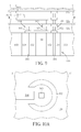
- FIG. 10A , FIG. 10B and FIG. 10C illustrate the top views of different layers in the multi-layer metal structure 160 .
- FIG. 10A illustrates the top view of the A-A′ plane as illustrated in FIG. 9 .
- FIG. 10B illustrates the top view of the B-B′ plane as illustrated in FIG. 9 .
- FIG. 10C illustrates the top view of the C-C′ plane as illustrated in FIG. 9 .
- the shapes of the third conductive structure 163 and the second conductive structure 162 are not limited to the above examples. Any shape will do as long as the shape has an effective electrical connection and shielding effect.
- the first conductive structure 161 , the second conductive structure 162 and the third conductive structure 163 in the multi-layer metal structure 160 may respectively include multiple layers.
- the first conductive structure 161 may at most include 1 to m ⁇ 1 th layer
- the third conductive structure 163 may at least include 1 to m+1 th layer.
- the conductive layer extension part 165 may have a curved structure 167 , such as a serpent-like or zigzag structure to transport the signal to the topmost layer.
- the wafer 103 includes a substrate 103 , a first side 101 and a second side 102 .
- the through via 115 is disposed in the wafer 103 to connect the first side 101 and the second side 102 .
- the through-silicon via structure 100 of the present invention is characterized in the composite annular structure 110 .
- the composite annular structure 110 includes at least a core conductive material 150 , a through via dielectric ring 112 , a first substrate ring 113 or a first conductive ring 151 , and a first dielectric ring 114 .
- the first conductive ring 151 includes a first conductive material 151 .
- the composite annular structure 110 is usually a concentric structure.
- the core conductive layer 150 usually includes a low-resistant material, such as copper.
- the core conductive layer 150 of the through-silicon via structure 100 fills up the through via 115 and may be in a form of a column with a diameter of 5 ⁇ m-20 ⁇ m. A smaller column facilitates increasing the element density of the entire wafer.
- the through via dielectric ring 112 may include a dielectric material, such as silicon oxide, and surrounds and directly contacts the core substrate column 111 .
- the first substrate ring 113 or the first conductive ring 151 is located outside of the through via dielectric ring 112 so it surrounds and directly contacts the through via dielectric ring 112 .
- the first dielectric ring 114 may include a dielectric material, such as silicon oxide, and is located outside of the first substrate ring 113 or the first conductive ring 151 so it surrounds and directly contacts the first substrate ring 113 or the first conductive ring 151 and it is at the same time surrounded by the semiconductor substrate 103 in the wafer.
- the core conductive layer 150 and first conductive material 151 may be the same or different from each other.
- the ring thickness of the through via dielectric ring 112 and the first dielectric ring 114 in the composite annular structure 110 may be 2 ⁇ m-3 ⁇ m.
- At least a set of concentric conductive ring and dielectric ring may be formed outside of the first dielectric ring 114 .
- a second conductive ring 152 and a second dielectric ring 117 are formed.
- the second conductive ring 152 surrounds and directly contacts the first dielectric ring 114 .
- the second dielectric ring 117 surrounds and directly contacts the second conductive ring 152 , and is surrounded by the wafer 103 .
- the semiconductor element 120 may include a gate 123 , and a source 121 and a drain 122 disposed adjacent to the gate 123 .
- the interconnection structure 125 penetrates the interlayer dielectric layer 124 and is electrically connected to the corresponding source 121 , the drain 122 and the gate 123 on the first side 101 through some contact plugs 126 .
- the interconnection structure 125 may be a multi-layer metal structure 160 .
- the multi-layer metal structure 160 may be disposed on the first side 101 and includes a first conductive structure 161 , a second conductive structure 162 and a third conductive structure 163 .
- the second conductive structure 162 and the third conductive structure 163 may respectively have a void.
- the third conductive structure 163 may be a ring with a void which allows the second conductive structure 162 to pass through.
- the second conductive structure 162 may be a round with a void which allows the first conductive structure 161 to pass through. In such a way, the needed multi-layer metal structure 160 is constructed.
- the first conductive material 151 may form the first conductive ring first extension part 164 with the first conductive structure 161 so the first conductive ring first extension part 164 is formed from the first conductive structure 161 .
- the first conductive material 151 may form the first conductive ring third extension part 166 with the third conductive structure 163 so the first conductive ring third extension part 166 is formed from the third conductive structure 163 .
- the second conductive structure 162 in the multi-layer metal structure 160 forms a conductive layer second extension part 165 . In such a way, the first conductive ring first extension part 164 and the first conductive ring third extension part 166 together sandwich the conductive layer second extension part 165 to shield the adverse interaction between the wafer 103 and the conductive layer second extension part 165 .
- the first conductive structure 161 , the second conductive structure 162 and the third conductive structure 163 in the multi-layer metal structure 160 may respectively include multiple layers.
- the layers of the second conductive structure 162 are more than that of the first conductive structure 161 , but less than these of the third conductive structure 163 .
- the conductive layer extension part 165 may have a curved structure 167 , such as a serpent-like or zigzag structure so that the conductive layer extension part 165 always extends upwards to transport the signal to the topmost layer.
- FIG. 10A , FIG. 10B and FIG. 10C illustrate the top views of different layers in the multi-layer metal structure 160 .
- FIG. 10A illustrates the top view of the A-A′ plane as illustrated in FIG. 9 .
- FIG. 10B illustrates the top view of the B-B′ plane as illustrated in FIG. 9 .
- FIG. 10C illustrates the top view of the C-C′ plane as illustrated in FIG. 9 .
- the shapes of the third conductive structure 163 and the second conductive structure 162 are not limited to the above examples. Any shape will do as long as the shape has an effective electrical connection and shielding effect.
- the core conductive material 150 and the first substrate ring 113 or the first conductive ring 151 may be respectively electrically connected to a suitable voltage by the interconnection structure.
- the first substrate ring 113 and the first conductive ring 151 is useful in shielding the adverse electrical coupling effect between the conductive substrate 101 in the wafer and the core conductive material 150 in the through-silicon via structure 100 .
- the core conductive material 150 is electrically connected to a core voltage, namely Vc
- the first substrate ring 113 or the first conductive ring 151 may be electrically connected to a first voltage, namely Vf.
- Vc and Vf may be the same or close to each other. Or, Vc and Vf may be different. For example, Vf may be half of Vc. Suitable values of Vc and Vf are in accordance with the practice of the present invention.
- the interconnection structure which connects the first conductive ring 151 or the first substrate ring 113 to a suitable voltage may be an annular structure which surrounds the core conductive material 150 without in direct contact with it.
- the core column in the composite annular structure 110 is not necessarily a conductive material.
- the core column may also be an insulting dielectric material column 112 .
- the insulting dielectric material column 112 is surrounded by a first substrate ring 113 or a conductive ring.
- the first substrate ring 113 or a conductive ring is surrounded by a first dielectric ring 114 .
- the first dielectric ring 114 is surrounded by another substrate ring or a second conductive ring 152 .
- the second conductive ring 152 or a conductive ring is surrounded by a second dielectric ring 117 and the second dielectric ring 117 is surrounded by the substrate in the wafer 103 .
Landscapes
- Internal Circuitry In Semiconductor Integrated Circuit Devices (AREA)
Abstract
Description
Claims (21)
Priority Applications (1)
| Application Number | Priority Date | Filing Date | Title |
|---|---|---|---|
| US13/085,488 US8519515B2 (en) | 2011-04-13 | 2011-04-13 | TSV structure and method for forming the same |
Applications Claiming Priority (1)
| Application Number | Priority Date | Filing Date | Title |
|---|---|---|---|
| US13/085,488 US8519515B2 (en) | 2011-04-13 | 2011-04-13 | TSV structure and method for forming the same |
Publications (2)
| Publication Number | Publication Date |
|---|---|
| US20120261826A1 US20120261826A1 (en) | 2012-10-18 |
| US8519515B2 true US8519515B2 (en) | 2013-08-27 |
Family
ID=47005836
Family Applications (1)
| Application Number | Title | Priority Date | Filing Date |
|---|---|---|---|
| US13/085,488 Active 2031-07-21 US8519515B2 (en) | 2011-04-13 | 2011-04-13 | TSV structure and method for forming the same |
Country Status (1)
| Country | Link |
|---|---|
| US (1) | US8519515B2 (en) |
Cited By (9)
| Publication number | Priority date | Publication date | Assignee | Title |
|---|---|---|---|---|
| US20120049322A1 (en) * | 2010-09-01 | 2012-03-01 | Taiwan Semiconductor Manufacturing Company, Ltd. | Cylindrical Embedded Capacitors |
| US20140087548A1 (en) * | 2011-07-29 | 2014-03-27 | Taiwan Semiconductor Manufacturing Company, Ltd. | Method of shielding through silicon vias in a passive interposer |
| US8772946B2 (en) * | 2012-06-08 | 2014-07-08 | Invensas Corporation | Reduced stress TSV and interposer structures |
| US8916979B2 (en) * | 2012-12-28 | 2014-12-23 | Taiwan Semiconductor Manufacturing Company, Ltd. | Through-vias and methods of forming the same |
| US9378778B1 (en) | 2015-06-14 | 2016-06-28 | Darryl G. Walker | Package including a plurality of stacked semiconductor devices including a capacitance enhanced through via and method of manufacture |
| US20170250112A1 (en) * | 2016-02-26 | 2017-08-31 | Infineon Technologies Ag | Semiconductor device and a method for forming a semiconductor device |
| US9911689B2 (en) * | 2013-12-23 | 2018-03-06 | Intel Corporation | Through-body-via isolated coaxial capacitor and techniques for forming same |
| US20230275012A1 (en) * | 2022-02-28 | 2023-08-31 | Taiwan Semiconductor Manufacturing Company, Ltd. | Dielectric anchors for anchoring a conductive pillar |
| US20240063099A1 (en) * | 2022-08-16 | 2024-02-22 | Taiwan Semiconductor Manufacturing Company, Ltd. | Reduction of cracks in redistribution structure |
Families Citing this family (19)
| Publication number | Priority date | Publication date | Assignee | Title |
|---|---|---|---|---|
| KR101374338B1 (en) * | 2007-11-14 | 2014-03-14 | 삼성전자주식회사 | semicondoctor device having through-via and method of forming the same |
| US20130015504A1 (en) * | 2011-07-11 | 2013-01-17 | Chien-Li Kuo | Tsv structure and method for forming the same |
| US8541883B2 (en) * | 2011-11-29 | 2013-09-24 | Advanced Semiconductor Engineering, Inc. | Semiconductor device having shielded conductive vias |
| JP2013115382A (en) * | 2011-11-30 | 2013-06-10 | Elpida Memory Inc | Semiconductor device and manufacturing method thereof |
| US8546953B2 (en) * | 2011-12-13 | 2013-10-01 | Taiwan Semiconductor Manufacturing Co., Ltd. | Through silicon via (TSV) isolation structures for noise reduction in 3D integrated circuit |
| US9275933B2 (en) | 2012-06-19 | 2016-03-01 | United Microelectronics Corp. | Semiconductor device |
| KR101965906B1 (en) * | 2012-07-12 | 2019-04-04 | 에스케이하이닉스 주식회사 | Semiconductor device |
| US9105701B2 (en) * | 2013-06-10 | 2015-08-11 | Micron Technology, Inc. | Semiconductor devices having compact footprints |
| US20160225694A1 (en) * | 2013-06-27 | 2016-08-04 | Hans-Joachim Barth | High conductivity high frequency via for electronic systems |
| US20150028482A1 (en) * | 2013-07-23 | 2015-01-29 | Globalfoundries Inc. | Device layout for reducing through-silicon-via stress |
| US9252077B2 (en) * | 2013-09-25 | 2016-02-02 | Intel Corporation | Package vias for radio frequency antenna connections |
| US9793204B2 (en) * | 2015-11-17 | 2017-10-17 | Taiwan Semiconductor Manufacturing Company Limited | Method of manufacturing semiconductor structure comprising plurality of through holes using metal hard mask |
| US10607885B2 (en) * | 2016-03-30 | 2020-03-31 | Intel Corporation | Shell structure for insulation of a through-substrate interconnect |
| DE102016219275B3 (en) * | 2016-10-05 | 2017-08-10 | Ihp Gmbh - Innovations For High Performance Microelectronics / Leibniz-Institut Für Innovative Mikroelektronik | Technological method for the prevention of vertical / lateral inhomogeneities in the etching of silicon vias by means of buried etch stop layers |
| US9974201B1 (en) * | 2016-10-28 | 2018-05-15 | General Electric Company | High power feedthrough for use with a high frequency power converter |
| US11495559B2 (en) * | 2020-04-27 | 2022-11-08 | Taiwan Semiconductor Manufacturing Company, Ltd. | Integrated circuits |
| US11990390B2 (en) * | 2020-07-06 | 2024-05-21 | Changxin Memory Technologies, Inc. | Semiconductor structure |
| CN112397444A (en) * | 2020-11-16 | 2021-02-23 | 西安电子科技大学 | Low-crosstalk silicon through hole structure and manufacturing method thereof |
| CN114566478B (en) * | 2022-04-28 | 2022-08-05 | 武汉大学 | Coaxial double-ring TSV structure with low thermal stress and high electrical property and preparation method |
Citations (32)
| Publication number | Priority date | Publication date | Assignee | Title |
|---|---|---|---|---|
| US5229647A (en) | 1991-03-27 | 1993-07-20 | Micron Technology, Inc. | High density data storage using stacked wafers |
| US5399898A (en) | 1992-07-17 | 1995-03-21 | Lsi Logic Corporation | Multi-chip semiconductor arrangements using flip chip dies |
| US5463246A (en) | 1988-12-29 | 1995-10-31 | Sharp Kabushiki Kaisha | Large scale high density semiconductor apparatus |
| US5484073A (en) | 1994-03-28 | 1996-01-16 | I/O Sensors, Inc. | Method for fabricating suspension members for micromachined sensors |
| US20020017399A1 (en) * | 2000-08-11 | 2002-02-14 | Huey-Ru Chang | Coaxial via hole and process of fabricating the same |
| US6407002B1 (en) | 2000-08-10 | 2002-06-18 | Taiwan Semiconductor Manufacturing Company | Partial resist free approach in contact etch to improve W-filling |
| US6548891B2 (en) | 2000-10-24 | 2003-04-15 | Shinko Electric Industries Co., Ltd. | Semiconductor device and production process thereof |
| US6627985B2 (en) | 2001-12-05 | 2003-09-30 | Arbor Company Llp | Reconfigurable processor module comprising hybrid stacked integrated circuit die elements |
| US20040080041A1 (en) | 2002-10-21 | 2004-04-29 | Nec Electronics Corporation | Semiconductor device with improved heatsink structure |
| US6800930B2 (en) | 2002-07-31 | 2004-10-05 | Micron Technology, Inc. | Semiconductor dice having back side redistribution layer accessed using through-silicon vias, and assemblies |
| US6924551B2 (en) | 2003-05-28 | 2005-08-02 | Intel Corporation | Through silicon via, folded flex microelectronic package |
| US7034401B2 (en) | 2003-12-17 | 2006-04-25 | Tru-Si Technologies, Inc. | Packaging substrates for integrated circuits and soldering methods |
| US7033934B2 (en) * | 2001-11-07 | 2006-04-25 | Shinko Electric Industries Co., Ltd. | Method of production of semiconductor package |
| US20070126085A1 (en) | 2005-12-02 | 2007-06-07 | Nec Electronics Corporation | Semiconductor device and method of manufacturing the same |
| US20070161235A1 (en) * | 2005-06-14 | 2007-07-12 | John Trezza | Back-to-front via process |
| US20070190692A1 (en) | 2006-01-13 | 2007-08-16 | Mete Erturk | Low resistance and inductance backside through vias and methods of fabricating same |
| US7282951B2 (en) | 2001-12-05 | 2007-10-16 | Arbor Company Llp | Reconfigurable processor module comprising hybrid stacked integrated circuit die elements |
| US20080073747A1 (en) | 2006-09-22 | 2008-03-27 | Clinton Chao | Electromagnetic shielding using through-silicon vias |
| US20080079131A1 (en) * | 2006-09-30 | 2008-04-03 | Sung Min Kim | Stack package and method for manufacturing the same |
| US7432592B2 (en) | 2005-10-13 | 2008-10-07 | Intel Corporation | Integrated micro-channels for 3D through silicon architectures |
| US7531415B2 (en) | 2000-11-30 | 2009-05-12 | Texas Instruments Incorporated | Multilayered CMP stop for flat planarization |
| US20090134498A1 (en) | 2007-11-20 | 2009-05-28 | Elpida Memory, Inc. | Semiconductor apparatus |
| US20090189256A1 (en) * | 2008-01-29 | 2009-07-30 | Yasuhiro Yoshimura | Manufacturing process of semiconductor device and semiconductor device |
| US20100072579A1 (en) * | 2008-09-23 | 2010-03-25 | Andreas Thies | Through Substrate Conductors |
| US20100140749A1 (en) | 2008-12-08 | 2010-06-10 | Chien-Li Kuo | Semiconductor device |
| US20100224965A1 (en) * | 2009-03-09 | 2010-09-09 | Chien-Li Kuo | Through-silicon via structure and method for making the same |
| US7932584B2 (en) * | 2005-06-14 | 2011-04-26 | Cufer Asset Ltd. L.L.C. | Stacked chip-based system and method |
| US7964972B2 (en) * | 2004-06-30 | 2011-06-21 | Renesas Electronics Corporation | Semiconductor device providing a first electrical conductor and a second electrical conductor in one through hole and method for manufacturing the same |
| US20110171829A1 (en) * | 2007-12-04 | 2011-07-14 | Advanced Semiconductor Engineering, Inc. | Method for Forming a Via in a Substrate and Substrate with a Via |
| US8148824B2 (en) * | 2010-04-16 | 2012-04-03 | Nanya Technology Corp. | Semiconductor device with through substrate via |
| US20120112324A1 (en) * | 2005-05-18 | 2012-05-10 | Kolo Technologies, Inc. | Through-wafer interconnection |
| US8384207B2 (en) * | 2005-08-26 | 2013-02-26 | Honda Motor Co., Ltd. | Semiconductor integrated circuit device having insulated through wires |
-
2011
- 2011-04-13 US US13/085,488 patent/US8519515B2/en active Active
Patent Citations (36)
| Publication number | Priority date | Publication date | Assignee | Title |
|---|---|---|---|---|
| US5463246A (en) | 1988-12-29 | 1995-10-31 | Sharp Kabushiki Kaisha | Large scale high density semiconductor apparatus |
| US5229647A (en) | 1991-03-27 | 1993-07-20 | Micron Technology, Inc. | High density data storage using stacked wafers |
| US5399898A (en) | 1992-07-17 | 1995-03-21 | Lsi Logic Corporation | Multi-chip semiconductor arrangements using flip chip dies |
| US5484073A (en) | 1994-03-28 | 1996-01-16 | I/O Sensors, Inc. | Method for fabricating suspension members for micromachined sensors |
| US6407002B1 (en) | 2000-08-10 | 2002-06-18 | Taiwan Semiconductor Manufacturing Company | Partial resist free approach in contact etch to improve W-filling |
| US20020017399A1 (en) * | 2000-08-11 | 2002-02-14 | Huey-Ru Chang | Coaxial via hole and process of fabricating the same |
| US6548891B2 (en) | 2000-10-24 | 2003-04-15 | Shinko Electric Industries Co., Ltd. | Semiconductor device and production process thereof |
| US7531415B2 (en) | 2000-11-30 | 2009-05-12 | Texas Instruments Incorporated | Multilayered CMP stop for flat planarization |
| US7033934B2 (en) * | 2001-11-07 | 2006-04-25 | Shinko Electric Industries Co., Ltd. | Method of production of semiconductor package |
| US7282951B2 (en) | 2001-12-05 | 2007-10-16 | Arbor Company Llp | Reconfigurable processor module comprising hybrid stacked integrated circuit die elements |
| US6627985B2 (en) | 2001-12-05 | 2003-09-30 | Arbor Company Llp | Reconfigurable processor module comprising hybrid stacked integrated circuit die elements |
| US6800930B2 (en) | 2002-07-31 | 2004-10-05 | Micron Technology, Inc. | Semiconductor dice having back side redistribution layer accessed using through-silicon vias, and assemblies |
| US20040080041A1 (en) | 2002-10-21 | 2004-04-29 | Nec Electronics Corporation | Semiconductor device with improved heatsink structure |
| US6924551B2 (en) | 2003-05-28 | 2005-08-02 | Intel Corporation | Through silicon via, folded flex microelectronic package |
| US7034401B2 (en) | 2003-12-17 | 2006-04-25 | Tru-Si Technologies, Inc. | Packaging substrates for integrated circuits and soldering methods |
| US20110210426A1 (en) * | 2004-06-30 | 2011-09-01 | Renesas Electronics Corporation | Semiconductor device providing a first electrical conductor and a second electrical conductor in one through hole and method for manufacturing the same |
| US7964972B2 (en) * | 2004-06-30 | 2011-06-21 | Renesas Electronics Corporation | Semiconductor device providing a first electrical conductor and a second electrical conductor in one through hole and method for manufacturing the same |
| US20120112324A1 (en) * | 2005-05-18 | 2012-05-10 | Kolo Technologies, Inc. | Through-wafer interconnection |
| US7932584B2 (en) * | 2005-06-14 | 2011-04-26 | Cufer Asset Ltd. L.L.C. | Stacked chip-based system and method |
| US20070161235A1 (en) * | 2005-06-14 | 2007-07-12 | John Trezza | Back-to-front via process |
| US8384207B2 (en) * | 2005-08-26 | 2013-02-26 | Honda Motor Co., Ltd. | Semiconductor integrated circuit device having insulated through wires |
| US7432592B2 (en) | 2005-10-13 | 2008-10-07 | Intel Corporation | Integrated micro-channels for 3D through silicon architectures |
| US20070126085A1 (en) | 2005-12-02 | 2007-06-07 | Nec Electronics Corporation | Semiconductor device and method of manufacturing the same |
| US20070190692A1 (en) | 2006-01-13 | 2007-08-16 | Mete Erturk | Low resistance and inductance backside through vias and methods of fabricating same |
| US20080073747A1 (en) | 2006-09-22 | 2008-03-27 | Clinton Chao | Electromagnetic shielding using through-silicon vias |
| US7525186B2 (en) * | 2006-09-30 | 2009-04-28 | Hynix Semiconductor Inc. | Stack package having guard ring which insulates through-via interconnection plug and method for manufacturing the same |
| US20080079131A1 (en) * | 2006-09-30 | 2008-04-03 | Sung Min Kim | Stack package and method for manufacturing the same |
| US20090134498A1 (en) | 2007-11-20 | 2009-05-28 | Elpida Memory, Inc. | Semiconductor apparatus |
| US20110171829A1 (en) * | 2007-12-04 | 2011-07-14 | Advanced Semiconductor Engineering, Inc. | Method for Forming a Via in a Substrate and Substrate with a Via |
| US20090189256A1 (en) * | 2008-01-29 | 2009-07-30 | Yasuhiro Yoshimura | Manufacturing process of semiconductor device and semiconductor device |
| US20100072579A1 (en) * | 2008-09-23 | 2010-03-25 | Andreas Thies | Through Substrate Conductors |
| US20100140749A1 (en) | 2008-12-08 | 2010-06-10 | Chien-Li Kuo | Semiconductor device |
| US20100224965A1 (en) * | 2009-03-09 | 2010-09-09 | Chien-Li Kuo | Through-silicon via structure and method for making the same |
| US8168533B2 (en) * | 2009-03-09 | 2012-05-01 | United Microelectronics Corp. | Through-silicon via structure and method for making the same |
| US8148824B2 (en) * | 2010-04-16 | 2012-04-03 | Nanya Technology Corp. | Semiconductor device with through substrate via |
| US8202801B1 (en) * | 2010-04-16 | 2012-06-19 | Nanya Technology Corp. | Method of fabricating a semiconductor device with through substrate via |
Cited By (21)
| Publication number | Priority date | Publication date | Assignee | Title |
|---|---|---|---|---|
| US20120049322A1 (en) * | 2010-09-01 | 2012-03-01 | Taiwan Semiconductor Manufacturing Company, Ltd. | Cylindrical Embedded Capacitors |
| US8693163B2 (en) * | 2010-09-01 | 2014-04-08 | Taiwan Semiconductor Manufacturing Company, Ltd. | Cylindrical embedded capacitors |
| US9691840B2 (en) | 2010-09-01 | 2017-06-27 | Taiwan Semiconductor Manufacturing Company, Ltd. | Cylindrical embedded capacitors |
| US20140087548A1 (en) * | 2011-07-29 | 2014-03-27 | Taiwan Semiconductor Manufacturing Company, Ltd. | Method of shielding through silicon vias in a passive interposer |
| US9159564B2 (en) * | 2011-07-29 | 2015-10-13 | Taiwan Semiconductor Manufacturing Company, Ltd. | Method of shielding through silicon vias in a passive interposer |
| US9000600B2 (en) | 2012-06-08 | 2015-04-07 | Invensas Corporation | Reduced stress TSV and interposer structures |
| US9349669B2 (en) | 2012-06-08 | 2016-05-24 | Invensas Corporation | Reduced stress TSV and interposer structures |
| US8772946B2 (en) * | 2012-06-08 | 2014-07-08 | Invensas Corporation | Reduced stress TSV and interposer structures |
| US11682583B2 (en) | 2012-12-28 | 2023-06-20 | Taiwan Semiconductor Manufacturing Company, Ltd. | Through-vias and methods of forming the same |
| US8916979B2 (en) * | 2012-12-28 | 2014-12-23 | Taiwan Semiconductor Manufacturing Company, Ltd. | Through-vias and methods of forming the same |
| US10157791B2 (en) | 2012-12-28 | 2018-12-18 | Taiwan Semiconductor Manufacturing Company, Ltd. | Through-vias and methods of forming the same |
| US9911689B2 (en) * | 2013-12-23 | 2018-03-06 | Intel Corporation | Through-body-via isolated coaxial capacitor and techniques for forming same |
| TWI662685B (en) * | 2013-12-23 | 2019-06-11 | Intel Corporation | Through-body-via isolated coaxial capacitor and techniques for forming same |
| US9455189B1 (en) * | 2015-06-14 | 2016-09-27 | Darryl G. Walker | Package including a plurality of stacked semiconductor devices including a capacitance enhanced through via and method of manufacture |
| US9378778B1 (en) | 2015-06-14 | 2016-06-28 | Darryl G. Walker | Package including a plurality of stacked semiconductor devices including a capacitance enhanced through via and method of manufacture |
| US9875934B2 (en) * | 2016-02-26 | 2018-01-23 | Infineon Technologies Ag | Semiconductor device and a method for forming a semiconductor device |
| US20170250112A1 (en) * | 2016-02-26 | 2017-08-31 | Infineon Technologies Ag | Semiconductor device and a method for forming a semiconductor device |
| US20230275012A1 (en) * | 2022-02-28 | 2023-08-31 | Taiwan Semiconductor Manufacturing Company, Ltd. | Dielectric anchors for anchoring a conductive pillar |
| US12170243B2 (en) * | 2022-02-28 | 2024-12-17 | Taiwan Semiconductor Manufacturing Company, Ltd. | Dielectric anchors for anchoring a conductive pillar |
| US20240063099A1 (en) * | 2022-08-16 | 2024-02-22 | Taiwan Semiconductor Manufacturing Company, Ltd. | Reduction of cracks in redistribution structure |
| US12476178B2 (en) * | 2022-08-16 | 2025-11-18 | Taiwan Semiconductor Manufacturing Company, Ltd. | Reduction of cracks in redistribution structure |
Also Published As
| Publication number | Publication date |
|---|---|
| US20120261826A1 (en) | 2012-10-18 |
Similar Documents
| Publication | Publication Date | Title |
|---|---|---|
| US8519515B2 (en) | TSV structure and method for forming the same | |
| US8168533B2 (en) | Through-silicon via structure and method for making the same | |
| US10431546B2 (en) | Manufacturing method for semiconductor device and semiconductor device | |
| TWI503981B (en) | Semiconductor device | |
| US8202766B2 (en) | Method for fabricating through-silicon via structure | |
| US20130015504A1 (en) | Tsv structure and method for forming the same | |
| US8809188B2 (en) | Method for fabricating through substrate vias | |
| TWI525776B (en) | Optimized ring-shaped copper through-substrate perforation | |
| US8421238B2 (en) | Stacked semiconductor device with through via | |
| US8481425B2 (en) | Method for fabricating through-silicon via structure | |
| CN102301465B (en) | Through-substrate vias | |
| TWI732269B (en) | Pad structure for enhanced bondability and method of forming the same | |
| CN102468284B (en) | Stacked semiconductor device and method of manufacturing the same | |
| CN103137566B (en) | Method for forming integrated circuit | |
| CN103515302B (en) | Semiconductor device and method of manufacture | |
| CN102760710B (en) | Through-silicon via structure and method for forming the same | |
| US8822336B2 (en) | Through-silicon via forming method | |
| CN104733381A (en) | Wafer through silicon via interconnection process | |
| TWI546866B (en) | Semiconductor device and fabricating method thereof | |
| CN111916392A (en) | Manufacturing method of semiconductor device | |
| CN112530899B (en) | Semiconductor device and method for manufacturing the same | |
| TWI518861B (en) | Tsv structure and method for forming the same | |
| US9287173B2 (en) | Through silicon via and process thereof |
Legal Events
| Date | Code | Title | Description |
|---|---|---|---|
| AS | Assignment |
Owner name: UNITED MICROELECTRONICS CORP., TAIWAN Free format text: ASSIGNMENT OF ASSIGNORS INTEREST;ASSIGNORS:KUO, CHIEN-LI;LIN, CHIA-FANG;REEL/FRAME:026112/0425 Effective date: 20110401 |
|
| STCF | Information on status: patent grant |
Free format text: PATENTED CASE |
|
| CC | Certificate of correction | ||
| FPAY | Fee payment |
Year of fee payment: 4 |
|
| MAFP | Maintenance fee payment |
Free format text: PAYMENT OF MAINTENANCE FEE, 8TH YEAR, LARGE ENTITY (ORIGINAL EVENT CODE: M1552); ENTITY STATUS OF PATENT OWNER: LARGE ENTITY Year of fee payment: 8 |
|
| AS | Assignment |
Owner name: MARLIN SEMICONDUCTOR LIMITED, IRELAND Free format text: ASSIGNMENT OF ASSIGNORS INTEREST;ASSIGNOR:UNITED MICROELECTRONICS CORPORATION;REEL/FRAME:056991/0292 Effective date: 20210618 Owner name: MARLIN SEMICONDUCTOR LIMITED, IRELAND Free format text: ASSIGNMENT OF ASSIGNOR'S INTEREST;ASSIGNOR:UNITED MICROELECTRONICS CORPORATION;REEL/FRAME:056991/0292 Effective date: 20210618 |
|
| MAFP | Maintenance fee payment |
Free format text: PAYMENT OF MAINTENANCE FEE, 12TH YEAR, LARGE ENTITY (ORIGINAL EVENT CODE: M1553); ENTITY STATUS OF PATENT OWNER: LARGE ENTITY Year of fee payment: 12 |