US8476923B2 - Impedance control circuit and integrated circuit chip including the same - Google Patents
Impedance control circuit and integrated circuit chip including the same Download PDFInfo
- Publication number
- US8476923B2 US8476923B2 US13/334,022 US201113334022A US8476923B2 US 8476923 B2 US8476923 B2 US 8476923B2 US 201113334022 A US201113334022 A US 201113334022A US 8476923 B2 US8476923 B2 US 8476923B2
- Authority
- US
- United States
- Prior art keywords
- impedance
- unit
- code
- voltage
- value
- Prior art date
- Legal status (The legal status is an assumption and is not a legal conclusion. Google has not performed a legal analysis and makes no representation as to the accuracy of the status listed.)
- Active
Links
Images
Classifications
-
- H—ELECTRICITY
- H03—ELECTRONIC CIRCUITRY
- H03K—PULSE TECHNIQUE
- H03K19/00—Logic circuits, i.e. having at least two inputs acting on one output; Inverting circuits
- H03K19/0005—Modifications of input or output impedance
-
- G—PHYSICS
- G11—INFORMATION STORAGE
- G11C—STATIC STORES
- G11C7/00—Arrangements for writing information into, or reading information out from, a digital store
- G11C7/10—Input/output [I/O] data interface arrangements, e.g. I/O data control circuits, I/O data buffers
Definitions
- Exemplary embodiments of the present invention relate to an impedance control circuit.
- the swing width of signals interfaced between semiconductor devices decrease gradually to minimize the delay time taken for signals to transfer.
- signal reflection originating from impedance mismatch at an interface node may affect the interfaced signal.
- the impedance mismatch is caused by external noise, variation of power source voltage, a change in operation temperature, a change in a fabrication process, and the like. Data may not be transferred at a fast rate due to the impedance mismatch.
- the impedance mismatch may distort data outputted from a data output end of a semiconductor device. Therefore, setup/hold failure and input-voltage level indecision may be frequently caused when the semiconductor device receives a distorted output signal through the semiconductor device input.
- a semiconductor device featuring a fast operation speed adopts an impedance matching circuit, which is referred to as an on-die termination, around a pad in an integrated circuit chip to address some of the above described issues in signal transfer.
- an on-die termination scheme a source termination is performed in an output circuit of a transferring part, and a parallel termination is performed in a termination circuit that is coupled in parallel to the reception circuit coupled with the input pad.
- ZQ calibration refers to a process for generating an impedance code that is used to maintain an impedance value at a target value although there is a change in the conditions of process, voltage and temperature (PVT).
- a termination impedance value is controlled based on the impedance code that is generated as a result of the ZQ calibration.
- a pad coupled with a reference resistor which becomes a reference of a calibration operation, is referred to as a ZQ pad.
- the reference resistor is commonly called an external resistor because it is coupled outside of a chip.
- the impedance control circuit for generating an impedance code is described.
- the impedance control circuit is also referred to as a calibration circuit.
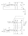
- FIG. 1 is a schematic view of a conventional impedance control circuit.
- the impedance control circuit includes a pull-up impedance unit 110 , a dummy impedance unit 120 , a pull-down impedance unit 130 , comparators 102 and 103 , and counters 104 and 105 .
- the comparator 102 compares the voltage of a calibration node ZQ with a reference voltage VREF and generates an up signal UP or a down signal DN based on the comparison result.
- the voltage of the calibration node ZQ is generated from voltage distribution of the pull-up impedance unit 110 and the external resistor 101 coupled with a calibration pad.
- the reference voltage VREF is usually set to VDD/2.
- the external resistor 101 is assumed to be of approximately 240 ⁇ .
- the counter 104 generates a pull-up impedance code PCODE ⁇ 0:N> in response to the up/down signal UP/DN.
- the pull-up impedance code PCODE ⁇ 0:N> adjusts the impedance value of the pull-up impedance unit 110 by turning on or off the parallel resistors inside of the pull-up impedance unit 110 .
- the parallel resistors are designed to have impedance values according to binary weight.
- the adjusted impedance value of the pull-up impedance unit 110 affects the voltage of the calibration node ZQ, and the above-described operation is repeated.
- the calibration operation repeats until the overall impedance value of the pull-up impedance unit 110 becomes the same as the impedance value of the external resistor 101 . This is referred to as pull-up calibration.
- the pull-up impedance code PCODE ⁇ 0:N> is inputted to the dummy impedance unit 120 to decide the impedance value of the dummy impedance unit 120 . From this point, a pull-down calibration operation begins. Just as the pull-up calibration operation, a calibration operation is performed using the comparator 103 and the counter 105 until the voltage of a node A becomes the same as the reference voltage VREF. This is referred to as pull-down calibration.
- the pull-up impedance code PCODE ⁇ 0:N> which makes the external resistor 101 and the pull-up impedance unit 110 have the same impedance value
- a pull-down impedance code NCODE ⁇ 0:N> which makes the dummy impedance unit 120 and the pull-down impedance unit 130 have the same impedance value
- the pull-up impedance code PCODE ⁇ 0:N> and the pull-down impedance code NCODE ⁇ 0:N> that are generated in the impedance control circuit are transferred to a termination circuit.
- the termination circuit terminates an interface code to adjust the impedance value of the termination circuit.
- the impedance value of the external resistor 101 is approximately 240 ⁇ , and the target impedance values of the pull-up impedance unit 110 and the pull-down impedance unit 130 are approximately 240 ⁇ too.
- the impedance value of the external resistor 101 and the target impedance values of the pull-up impedance unit 110 and the pull-down impedance unit 130 are the same.
- the calibration node ZQ may be coupled with an external resistor 101 having a different impedance value from the target impedance values of the pull-up impedance unit 110 and the pull-down impedance unit 130 .
- the target impedance values of the pull-up impedance unit 110 and the pull-down impedance unit 130 are approximately 240 ⁇ , but the calibration node ZQ may be coupled with an external resistor 101 having a resistance of approximately 960 ⁇ .
- An embodiment of the present invention is directed to an impedance control circuit that may generate accurate impedance codes even through the impedance value of an external resistor coupled with the impedance control circuit is different from the target impedance values of a pull-up impedance unit and a pull-down impedance unit.
- an impedance control circuit includes: a first impedance unit having an impedance value based on a first impedance code and configured to drive a first node coupled with an resistor outside of the integrated circuit chip with a first voltage; a first code generation unit configured to generate the first impedance code so that an impedance value of the first impedance unit and an impedance value of the resistor outside of the integrated circuit chip are at a ratio of X:Y, where X and Y are different numbers; a plurality of dummy impedance units that receive the first impedance code and drive a second node with the first voltage level; a second impedance unit having an impedance value based on a second impedance code and configured to drive the second node with a second voltage; and a second code generation unit configured to generate the second impedance code so that an overall impedance value of the dummy impedance units and an impedance value of the second impedance unit are at a ratio
- the ratio of X:Y may be a ratio of a target impedance value of the first impedance unit to an impedance value of the resistor outside of the integrated circuit chip.
- the number of the dummy impedance units may be Y/X.
- an integrated circuit chip includes: a first impedance unit having an impedance value based on a first impedance code and configured to drive a first node coupled with an resistor outside of the integrated circuit chip with a first voltage; a first code generation unit configured to generate the first impedance code so that an impedance value of the first impedance unit and an impedance value of the resistor outside of the integrated circuit chip are at a ratio of X:Y, where X and Y are different numbers; a plurality of dummy impedance units that receive the first impedance code and drive a second node with the first voltage; a second impedance unit having an impedance value based on a second impedance code and configured to drive the second node with a second voltage; a second code generation unit configured to generate the second impedance code so that an overall impedance value of the dummy impedance units and an impedance value of the second impedance unit are at a ratio of X:
- the ratio of X:Y may be a ratio of a target impedance value of the first impedance unit to an impedance value of the resistor outside of the integrated circuit chip.
- the number of the dummy impedance units may be Y/X.
- an impedance control circuit includes: a first impedance unit having an impedance value based on a first impedance code and configured to drive a first node coupled with an resistor outside of the integrated circuit chip with a first voltage; a first code generation unit configured to generate the first impedance code so that an impedance value of the first impedance unit and an impedance value of the resistor outside of the integrated circuit chip are at a ratio of X:Y, where X and Y are different numbers; a dummy impedance unit having an impedance value based on the first impedance code, where the impedance value is ⁇ (impedance value of the first impedance unit)*(X/Y) ⁇ and configured to drive a second node with the first voltage; a second impedance unit having an impedance value based on a second impedance code and configured to drive the second node with a second voltage; and a second code generation unit configured to generate the second impedance
- the first impedance unit may include: a plurality of first transistors that are turned on/off based on respective signals constituting the first impedance code; and a plurality of first resistors respectively coupled with the first transistors
- the dummy impedance unit may include: a plurality of second transistors that are turned on/off based on respective signals constituting the first impedance code; and a plurality of second resistors respectively coupled with the second transistors, the impedance value of the first resistors and the impedance value of the second resistors being at a ratio of X:Y.
- FIG. 1 is a schematic view of a conventional impedance control circuit.
- FIG. 2 is a schematic view of an impedance control circuit in accordance with an embodiment of the present invention.
- FIG. 3 illustrates a termination circuit for terminating an interface node based on impedance codes PCODE ⁇ 0:N> and NCODE ⁇ 0:N> that are generated in the impedance control circuit shown in FIG. 2 .
- FIG. 4 is a schematic view of an impedance control circuit in accordance with another embodiment of the present invention.
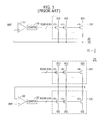
- FIG. 2 is a schematic view of an impedance control circuit in accordance with an embodiment of the present invention.
- the impedance control circuit includes a first impedance unit 210 , a first code generation unit 220 , a plurality of dummy impedance units 230 _ 0 to 230 _ 3 , a second impedance unit 240 , and a second code generation unit 250 .
- the technology of the present invention is directed to generating accurate impedance codes PCODE ⁇ 0:N> and NCODE ⁇ 0:N> when the target impedance values of the first impedance unit 210 and the second impedance unit 240 are different from the impedance value of an external resistor 201 .
- the target impedance values of the first impedance unit 210 and the second impedance unit 240 are approximately 240 ⁇ , and the impedance value of the external resistor 201 is approximately 960 ⁇ .
- a first voltage level is the voltage level of a power source voltage VDD
- a second voltage level is the voltage level of a ground voltage VSS.
- the first impedance unit 210 has an impedance value based on a first impedance code PCODE ⁇ 0:N>, and the first impedance unit 210 drives a first node ZQ coupled with the external resistor 201 with the first voltage level VDD.
- the first impedance unit 210 may include a plurality of transistors that are turned on or off based on the signals constituting the first impedance code PCODE ⁇ 0:N>, respectively.
- the first impedance unit 210 also includes a plurality of resistors that are respectively coupled with the transistors.
- the first code generation unit 220 generates the first impedance code PCODE ⁇ 0:N>.
- the first impedance code PCODE ⁇ 0:N> is generated to turn on an amount of the transistors in the first impedance unit 210 so that the impedance value of the first impedance unit 210 and the impedance value of the external resistor 201 are at a ratio of X:Y.
- the ratio of X:Y denotes the ratio of a target impedance value of the first impedance unit 210 to an impedance value of the external resistor 201 .
- the ratio of X:Y is exemplified as 1:4.
- the first code generation unit 220 includes a comparator 221 and a counter 222 .
- the comparator 221 compares the voltage level of the first node ZQ with the voltage level of a reference voltage VREF.
- the counter 222 generates the first impedance code PCODE ⁇ 0:N> in response to the comparison result of the comparator 221 .
- the reference voltage VREF is set to be VDD* ⁇ Y/(X+Y) ⁇ because the ratio of the impedance value of the first impedance unit 210 to the impedance value of the external resistor 201 is X:Y. In this embodiment of the present invention, the reference voltage is VDD*0.8.
- Each of the dummy impedance units 230 _ 0 to 230 _ 3 has a similar structure as the first impedance unit 210 . However, a second node A is driven with the first voltage level VDD instead of the first node ZQ.
- the number of the dummy impedance units 230 _ 0 to 230 _ 3 is Y/X, which is 4 in this embodiment of the present invention. The reason that the number of dummy impedance units is Y/X is because the ratio of the overall impedance value of the dummy impedance units 230 _ 0 to 230 _ 3 to the impedance value of the second impedance unit 240 is X:Y.
- the second impedance unit 240 has an impedance value based on a second impedance code NCODE ⁇ 0:N>, and the second impedance unit 240 drives the second node A with a second voltage level VSS.
- the second impedance unit 240 may include a plurality of transistors that are turned on or off based on the signals constituting the second impedance code NCODE ⁇ 0:N>, respectively.
- the second impedance unit may further include a plurality of resistors that are respectively coupled with the transistors.
- the second code generation unit 250 generates the second impedance code NCODE ⁇ 0:N>.
- the second impedance code NCODE ⁇ 0:N> is generated to turn on an amount of the transistors in the second impedance unit 240 so that the overall impedance value of the dummy impedance units 230 _ 0 to 230 _ 3 and the impedance value of the second impedance unit 240 are at the ratio of X:Y.
- the second code generation unit 250 includes a comparator 251 and a counter 252 .
- the comparator 251 compares the voltage level of the second node A with the voltage level of a reference voltage VREF.
- the counter 252 generates the second impedance code NCODE ⁇ 0:N> in response to the comparison result of the comparator 251 .
- the first code generation unit 220 generates the first impedance code PCODE ⁇ 0:N> in such a manner that the voltage level of the first node ZQ becomes the same as the voltage level of the reference voltage VREF. Therefore, the first impedance unit 210 receiving the first impedance code PCODE ⁇ 0:N> has an impedance value of approximately 240 ⁇ .
- the first impedance code PCODE ⁇ 0:N> is inputted to the dummy impedance units 230 _ 0 to 230 _ 3 , and therefore, each of the dummy impedance units 230 _ 0 to 230 _ 3 has an impedance value of approximately 240 ⁇ . Since the four dummy impedance units 230 _ 0 to 230 _ 3 are coupled in parallel to each other, the total impedance value of the dummy impedance units 230 _ 0 to 230 _ 3 results to approximately 60 ⁇ .
- the second code generation unit 250 generates the second impedance code NCODE ⁇ 0:N> in such a manner that the voltage level of the second node A becomes the same as the voltage level of the reference voltage VREF.
- the second impedance unit 240 comes to have an impedance value of approximately 240 ⁇ .
- the first impedance code PCODE ⁇ 0:N> and the second impedance code NCODE ⁇ 0:N> are generated in such a manner that the first impedance unit 210 and the second impedance unit 240 have the target impedance value of approximately 240 ⁇ .
- accurate impedance codes PCODE ⁇ 0:N> and NCODE ⁇ 0:N> may be generated by controlling the voltage level of the reference voltage VREF and the number of the dummy impedance units 230 _ 0 to 230 _ 3 .
- the embodiment of FIG. 2 exemplifies an impedance control circuit where the first voltage level is the voltage level of a power source voltage VDD while the second voltage level is the voltage level of a ground voltage VSS, and the first impedance code is a pull-up impedance code PCODE ⁇ 0:N> while the second impedance code is a pull-down impedance code NCODE ⁇ 0:N>.
- the first voltage level may be the voltage level of the ground voltage VSS while the second voltage level is the voltage level of the power source voltage VDD, and the first impedance code is a pull-down impedance code NCODE ⁇ 0:N> while the second impedance code is a pull-up impedance code PCODE ⁇ 0:N>.
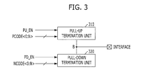
- FIG. 3 illustrates a termination circuit for terminating an interface node based on impedance codes PCODE ⁇ 0:N> and NCODE ⁇ 0:N> that are generated in the impedance control circuit shown in FIG. 2 .
- the interface node B is a node coupled with an interface pad INTERFACE through which data or signals are inputted/outputted.
- a ZQ pad includes the impedance control circuit (refer to FIG. 2 ) and an interface pad includes the termination circuit (refer to FIG. 3 ).
- the termination circuit includes a first termination unit 310 and a second termination unit 320 .
- the first termination unit 310 receives a first impedance code PCODE ⁇ 0:N> and has an impedance value based on the first impedance code PCODE ⁇ 0:N>.
- a PU_EN signal is inputted to the first termination unit 310 .
- the PU_EN signal is a signal for enabling the first termination unit 310 . In short, whether the first termination unit 310 is enabled or not is decided based on the PU_EN signal.
- the first termination unit 310 has an impedance value based on the first impedance code PCODE ⁇ 0:N>.
- the second termination unit 320 receives a second impedance code NCODE ⁇ 0:N> and has an impedance value based on the second impedance code NCODE ⁇ 0:N>.
- a PD_EN signal is inputted to the second termination unit 320 .
- the PD_EN signal is a signal for enabling the second termination unit 320 . In short, whether the second termination unit 320 is enabled or not is decided based on the PD_EN signal. When the second termination unit 320 is enabled, the second termination unit 320 has an impedance value based on the second impedance code NCODE ⁇ 0:N>.
- the termination circuit may include a plurality of first termination units 310 and a plurality of second termination units 320 according to the impedance value required for impedance matching. For example, if a pull-up impedance value and a pull-down impedance value have to be approximately 120 ⁇ , individually, two first termination units 310 having an impedance value of approximately 240 ⁇ are coupled with the interface node in parallel, and two second termination units 320 having an impedance value of approximately 240 ⁇ are coupled with the interface node in parallel.
- the first termination unit 310 and the second termination unit 320 have an internal structure similar to that of the first impedance unit 210 and the second impedance unit 240 , and the first termination unit 310 and the second termination unit 320 have almost the same impedance value as the first impedance unit 210 and the second impedance unit 240 .
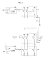
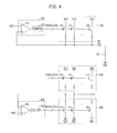
- FIG. 4 is a schematic view of an impedance control circuit in accordance with another embodiment of the present invention.
- the impedance control circuit includes a first impedance unit 410 , a first code generation unit 420 , a dummy impedance unit 430 , a second impedance unit 440 , and a second code generation unit 450 .
- the first impedance unit 410 has an impedance value based on a first impedance code PCODE ⁇ 0:N> and drives a first node ZQ coupled with an external resistor 401 with a first voltage level VDD.
- the first code generation unit 420 generates the first impedance code PCODE ⁇ 0:N>.
- the first impedance code PCODE ⁇ 0:N> is generated to turn on an amount of the transistors in the first impedance unit 410 so that an impedance value of the first impedance unit 410 and an impedance value of the external resistor 401 are at a ratio of X:Y, where X and Y are different numbers.
- the dummy impedance unit 430 has an impedance value based on the first impedance code PCODE ⁇ 0:N> where the impedance value is ⁇ (impedance value of the first impedance unit 410 )*(X/Y) ⁇ at the same code, and drives a second node A with the first voltage level VDD.
- the second impedance unit 440 has an impedance value based on a second impedance code NCODE ⁇ 0:N> and drives a second node A with the second voltage level VSS.
- the second code generation unit 450 generates the second impedance code NCODE ⁇ 0:N>.
- the second impedance code NCODE ⁇ 0:N> is generated to turn on an amount of the transistors in the second impedance unit 440 so that an impedance value of the dummy impedance unit 430 and an impedance value of the second impedance unit 440 are at a ratio of X:Ys.
- the dummy impedance unit 430 has the same structure as the first impedance unit 410 but has a different resistance value.
- the dummy impedance unit 430 has an impedance value of ⁇ (impedance value of the first impedance unit 410 )*(X/Y) ⁇ .
- X:Y is 1:4
- the dummy impedance unit 430 has an impedance value of (impedance value of the first impedance unit 410 )*1 ⁇ 4.
- the internal resistors of the dummy impedance unit 430 have 1 ⁇ 4 of the resistance value of the internal resistors of the first impedance unit 410 .
- the internal resistors of the dummy impedance unit 430 have 1 ⁇ 4 of the resistance value of the internal resistors of the first impedance unit 410 .
- four dummy impedance units 230 _ 0 to 230 _ 3 are provided to make the overall impedance value of the dummy impedance units 230 _ 0 to 230 _ 3 become (the impedance value of the first impedance unit 210 )*1 ⁇ 4, whereas the internal resistors of the dummy impedance unit 430 have lower resistance values than the internal resistors of the first and second impedance units 410 and 440 so that the impedance value of the dummy impedance unit 430 becomes (the impedance value of the first impedance unit 410 )*1 ⁇ 4 in the embodiment of FIG. 4 .
- an impedance control circuit may generate accurate impedance codes, even though the impedance value of an external resistor coupled with the impedance control circuit is different than the target impedance values of a pull-up impedance unit and a pull-down impedance unit.
Landscapes
- Physics & Mathematics (AREA)
- Engineering & Computer Science (AREA)
- Computer Hardware Design (AREA)
- Computing Systems (AREA)
- General Engineering & Computer Science (AREA)
- Mathematical Physics (AREA)
- Logic Circuits (AREA)
- Semiconductor Integrated Circuits (AREA)
- Dc Digital Transmission (AREA)
Applications Claiming Priority (2)
| Application Number | Priority Date | Filing Date | Title |
|---|---|---|---|
| KR1020110017666A KR101175245B1 (ko) | 2011-02-28 | 2011-02-28 | 임피던스 조절회로 및 이를 포함하는 집적회로 칩 |
| KR10-2011-0017666 | 2011-02-28 |
Publications (2)
| Publication Number | Publication Date |
|---|---|
| US20120217991A1 US20120217991A1 (en) | 2012-08-30 |
| US8476923B2 true US8476923B2 (en) | 2013-07-02 |
Family
ID=46718553
Family Applications (1)
| Application Number | Title | Priority Date | Filing Date |
|---|---|---|---|
| US13/334,022 Active US8476923B2 (en) | 2011-02-28 | 2011-12-21 | Impedance control circuit and integrated circuit chip including the same |
Country Status (2)
| Country | Link |
|---|---|
| US (1) | US8476923B2 (ko) |
| KR (1) | KR101175245B1 (ko) |
Cited By (2)
| Publication number | Priority date | Publication date | Assignee | Title |
|---|---|---|---|---|
| US20150109041A1 (en) * | 2012-08-30 | 2015-04-23 | SK Hynix Inc. | Method for reducing output data noise of semiconductor apparatus and semiconductor apparatus implementing the same |
| US11190185B2 (en) * | 2019-12-18 | 2021-11-30 | SK Hynix Inc. | Impedance calibration circuit and semiconductor apparatus including the same |
Families Citing this family (1)
| Publication number | Priority date | Publication date | Assignee | Title |
|---|---|---|---|---|
| US8415979B2 (en) * | 2010-11-04 | 2013-04-09 | Mediatek Inc. | Differential driver with calibration circuit and related calibration method |
Citations (3)
| Publication number | Priority date | Publication date | Assignee | Title |
|---|---|---|---|---|
| KR20090022043A (ko) | 2007-08-29 | 2009-03-04 | 주식회사 하이닉스반도체 | 온 다이 터미네이션 장치의 캘리브래이션 회로 |
| KR20100109143A (ko) | 2009-03-31 | 2010-10-08 | 주식회사 하이닉스반도체 | 빠른 동작을 하는 캘리브래이션 회로 |
| US7961001B1 (en) * | 2009-11-30 | 2011-06-14 | Hynix Semiconductor Inc. | Impedance adjusting device |
-
2011
- 2011-02-28 KR KR1020110017666A patent/KR101175245B1/ko active IP Right Grant
- 2011-12-21 US US13/334,022 patent/US8476923B2/en active Active
Patent Citations (3)
| Publication number | Priority date | Publication date | Assignee | Title |
|---|---|---|---|---|
| KR20090022043A (ko) | 2007-08-29 | 2009-03-04 | 주식회사 하이닉스반도체 | 온 다이 터미네이션 장치의 캘리브래이션 회로 |
| KR20100109143A (ko) | 2009-03-31 | 2010-10-08 | 주식회사 하이닉스반도체 | 빠른 동작을 하는 캘리브래이션 회로 |
| US7961001B1 (en) * | 2009-11-30 | 2011-06-14 | Hynix Semiconductor Inc. | Impedance adjusting device |
Non-Patent Citations (1)
| Title |
|---|
| Notice of Allowance issued by the Korean Intellectual Property Office on Jul. 29, 2012. |
Cited By (3)
| Publication number | Priority date | Publication date | Assignee | Title |
|---|---|---|---|---|
| US20150109041A1 (en) * | 2012-08-30 | 2015-04-23 | SK Hynix Inc. | Method for reducing output data noise of semiconductor apparatus and semiconductor apparatus implementing the same |
| US9124252B2 (en) * | 2012-08-30 | 2015-09-01 | SK Hynix Inc. | Method for reducing output data noise of semiconductor apparatus and semiconductor apparatus implementing the same |
| US11190185B2 (en) * | 2019-12-18 | 2021-11-30 | SK Hynix Inc. | Impedance calibration circuit and semiconductor apparatus including the same |
Also Published As
| Publication number | Publication date |
|---|---|
| US20120217991A1 (en) | 2012-08-30 |
| KR101175245B1 (ko) | 2012-08-21 |
Similar Documents
| Publication | Publication Date | Title |
|---|---|---|
| US7843211B2 (en) | Impedance adjusting circuit and semiconductor memory device having the same | |
| US9077332B2 (en) | Impedance control circuit and semiconductor device including the same | |
| US7961001B1 (en) | Impedance adjusting device | |
| US7893710B2 (en) | Termination circuit and impedance matching device including the same | |
| US7986161B2 (en) | Termination resistance circuit | |
| US7782078B2 (en) | On die termination circuit and method for calibrating the same | |
| US8120381B2 (en) | Impedance adjusting device | |
| KR100904482B1 (ko) | 온 다이 터미네이션 장치의 캘리브래이션 회로 | |
| KR100886644B1 (ko) | 온 다이 터미네이션 장치의 캘리브래이션 회로 | |
| US8319519B2 (en) | Impedance code generation circuit and integrated circuit including the same | |
| KR100863535B1 (ko) | 온 다이 터미네이션 장치 및 이를 포함하는 반도체메모리장치 | |
| US20100164540A1 (en) | Semiconductor Memory Device | |
| US20130162286A1 (en) | Impedance code generation circuit and semiconductor memory device including the same | |
| US8476923B2 (en) | Impedance control circuit and integrated circuit chip including the same | |
| KR100976414B1 (ko) | 캘리브래이션 회로, 온 다이 터미네이션 장치 및 반도체 메모리 장치 | |
| KR20090022043A (ko) | 온 다이 터미네이션 장치의 캘리브래이션 회로 | |
| US7772878B2 (en) | Parallel resistor circuit, on-die termination device having the same, and semiconductor memory device having the on-die termination device | |
| KR20120099908A (ko) | 임피던스 조절회로 | |
| KR20100109143A (ko) | 빠른 동작을 하는 캘리브래이션 회로 | |
| KR20090023833A (ko) | 온 다이 터미네이션 장치 |
Legal Events
| Date | Code | Title | Description |
|---|---|---|---|
| AS | Assignment |
Owner name: HYNIX SEMICONDUCTOR INC., KOREA, REPUBLIC OF Free format text: ASSIGNMENT OF ASSIGNORS INTEREST;ASSIGNORS:JANG, DONG-WOOK;KIM, YONG-MI;REEL/FRAME:027430/0297 Effective date: 20111006 |
|
| STCF | Information on status: patent grant |
Free format text: PATENTED CASE |
|
| FEPP | Fee payment procedure |
Free format text: PAYOR NUMBER ASSIGNED (ORIGINAL EVENT CODE: ASPN); ENTITY STATUS OF PATENT OWNER: LARGE ENTITY |
|
| FPAY | Fee payment |
Year of fee payment: 4 |
|
| MAFP | Maintenance fee payment |
Free format text: PAYMENT OF MAINTENANCE FEE, 8TH YEAR, LARGE ENTITY (ORIGINAL EVENT CODE: M1552); ENTITY STATUS OF PATENT OWNER: LARGE ENTITY Year of fee payment: 8 |