US8462608B2 - Read-only optical recording medium - Google Patents
Read-only optical recording medium Download PDFInfo
- Publication number
- US8462608B2 US8462608B2 US13/319,796 US201013319796A US8462608B2 US 8462608 B2 US8462608 B2 US 8462608B2 US 201013319796 A US201013319796 A US 201013319796A US 8462608 B2 US8462608 B2 US 8462608B2
- Authority
- US
- United States
- Prior art keywords
- data
- sub
- reflective film
- recording
- metal reflective
- Prior art date
- Legal status (The legal status is an assumption and is not a legal conclusion. Google has not performed a legal analysis and makes no representation as to the accuracy of the status listed.)
- Expired - Fee Related
Links
Images


Classifications
-
- G—PHYSICS
- G11—INFORMATION STORAGE
- G11B—INFORMATION STORAGE BASED ON RELATIVE MOVEMENT BETWEEN RECORD CARRIER AND TRANSDUCER
- G11B7/00—Recording or reproducing by optical means, e.g. recording using a thermal beam of optical radiation by modifying optical properties or the physical structure, reproducing using an optical beam at lower power by sensing optical properties; Record carriers therefor
- G11B7/007—Arrangement of the information on the record carrier, e.g. form of tracks, actual track shape, e.g. wobbled, or cross-section, e.g. v-shaped; Sequential information structures, e.g. sectoring or header formats within a track
- G11B7/00736—Auxiliary data, e.g. lead-in, lead-out, Power Calibration Area [PCA], Burst Cutting Area [BCA], control information
-
- G—PHYSICS
- G11—INFORMATION STORAGE
- G11B—INFORMATION STORAGE BASED ON RELATIVE MOVEMENT BETWEEN RECORD CARRIER AND TRANSDUCER
- G11B7/00—Recording or reproducing by optical means, e.g. recording using a thermal beam of optical radiation by modifying optical properties or the physical structure, reproducing using an optical beam at lower power by sensing optical properties; Record carriers therefor
- G11B7/24—Record carriers characterised by shape, structure or physical properties, or by the selection of the material
- G11B7/241—Record carriers characterised by shape, structure or physical properties, or by the selection of the material characterised by the selection of the material
- G11B7/252—Record carriers characterised by shape, structure or physical properties, or by the selection of the material characterised by the selection of the material of layers other than recording layers
- G11B7/258—Record carriers characterised by shape, structure or physical properties, or by the selection of the material characterised by the selection of the material of layers other than recording layers of reflective layers
- G11B7/2585—Record carriers characterised by shape, structure or physical properties, or by the selection of the material characterised by the selection of the material of layers other than recording layers of reflective layers based on aluminium
-
- Y—GENERAL TAGGING OF NEW TECHNOLOGICAL DEVELOPMENTS; GENERAL TAGGING OF CROSS-SECTIONAL TECHNOLOGIES SPANNING OVER SEVERAL SECTIONS OF THE IPC; TECHNICAL SUBJECTS COVERED BY FORMER USPC CROSS-REFERENCE ART COLLECTIONS [XRACs] AND DIGESTS
- Y10—TECHNICAL SUBJECTS COVERED BY FORMER USPC
- Y10T—TECHNICAL SUBJECTS COVERED BY FORMER US CLASSIFICATION
- Y10T428/00—Stock material or miscellaneous articles
- Y10T428/24—Structurally defined web or sheet [e.g., overall dimension, etc.]
- Y10T428/24479—Structurally defined web or sheet [e.g., overall dimension, etc.] including variation in thickness
- Y10T428/24521—Structurally defined web or sheet [e.g., overall dimension, etc.] including variation in thickness with component conforming to contour of nonplanar surface
- Y10T428/24545—Containing metal or metal compound
Definitions
- the present invention relates to a read-only optical recording medium including a metal reflective film.
- optical recording medium particularly a read-only ROM (Read Only Memory) disc
- ROM Read Only Memory
- optical recording media are widely used as package media.
- a method of adding identification information that differs for each disc is being considered.
- the method of adding identification information there is proposed a method of, for example, recording sub-data onto a metal reflective film (e.g., see Patent Document 1).
- an Ag (silver) alloy is used as the metal reflective film.
- the metal reflective film formed of an Ag alloy can be used not only in a read-only optical recording medium of Patent Document 1 that records sub-data, but also in a general read-only optical recording medium.
- Al or an Al alloy is used as a metal reflective film in an optical recording medium that records/reproduces information using light having wavelengths of 650 nm and 780 nm (see, for example, Patent Document 2).
- reflectance with respect to light having a wavelength of 405 nm is lowered by a temporal change.
- reproduction signal outputs vary due to the temporal change.
- a durable read-only optical recording medium having less variances in characteristics of a metal reflective film due to a temporal change is provided.
- a read-only optical recording medium including: a substrate; an information recording surface that is structured by combining pits and lands formed on the substrate and onto which information is recorded; and a metal reflective film that is provided in contact with the information recording surface and represented by Al 100-x-z X x Z z , where x and z each represent an atomic %, X is constituted of an element including at least Ti, Z is constituted of an element including at least Fe, x is 1.0 to 3.0, and z is 0.05 to 1.0.
- the metal reflective film is represented by Al 100-x-z X x Z z , where x and z each represent an atomic %, a content of the X component including at least Ti is 1.0 to 3.0, and a content of the Z component including at least Fe is 0.05 to 1.0.
- the metal reflective film can be formed of an inexpensive material.
- a durable read-only optical recording medium having less variances in characteristics of a metal reflective film due to a temporal change can be realized at low costs.
- FIG. 1 A schematic structural diagram (cross-sectional diagram) of a read-only optical recording medium according to a first embodiment of the present invention.
- FIG. 2 A Ti—Al-base phase diagram.
- FIG. 3 A diagram for explaining an embodiment of a production method for a read-only optical recording medium according to a second embodiment of the present invention.
- FIG. 4 A structural diagram showing an embodiment of a recording apparatus for sub-data that is used with respect to the read-only optical recording medium according to the second embodiment of the present invention.
- FIG. 5 An explanatory diagram for recording sub-data onto the read-only optical recording medium according to the second embodiment of the present invention.
- FIG. 6 A structural diagram showing an embodiment of a reproducing apparatus for sub-data that is used with respect to the read-only optical recording medium according to the second embodiment of the present invention.
- FIG. 7 An explanatory diagram for reproducing sub-data from the read-only optical recording medium according to the second embodiment of the present invention.
- FIGS. 8A and 8B are diagrams showing changes in reflectance before and after an acceleration test of the read-only optical recording medium according to Examples 1 and 2.
- FIGS. 9A and 9B are diagrams showing changes in the reflectance before and after the acceleration test of the read-only optical recording medium according to Comparative examples 1 and 2.
- FIG. 10 A diagram showing an initial recording sensitivity of the read-only optical recording medium according to Examples 3 to 7.
- FIG. 11 A diagram showing the initial recording sensitivity of the read-only optical recording medium according to Examples 8 to 12.
- FIG. 12 A diagram showing the initial recording sensitivity of the read-only optical recording medium according to Examples 13 to 17.
- FIG. 13 A diagram showing changes in a sub-data reproduction signal output before and after an acceleration test of the read-only optical recording medium according to Examples 3 to 7.
- FIG. 14 A diagram showing changes in the sub-data reproduction signal output before and after the acceleration test of the read-only optical recording medium according to Examples 8 to 12.
- FIG. 15 A diagram showing changes in the sub-data reproduction signal output before and after the acceleration test of the read-only optical recording medium according to Examples 13 to 17.
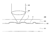
- FIG. 1 shows a schematic structural diagram (cross-sectional diagram) of a read-only optical recording medium according to a first embodiment of the present invention.
- An optical disc 100 has a multilayer structure in which a metal reflective film 102 and a cover layer 103 are laminated on a substrate 101 .
- a plastic substrate formed of, for example, polycarbonate can be used as the substrate 101 .
- a surface of the substrate 101 that comes into contact with the metal reflective film 102 has a concavo-convex cross-sectional shape.
- the concave cross-sectional portions correspond to pits P
- the convex cross-sectional portions correspond to lands L.
- the convex cross-sectional portions onto which laser light 105 is irradiated from the cover layer 103 and that protrude toward a light-incident side of the laser light 105 are the lands L.
- Information is recorded using a combination of the pits P and lands L, more specifically, lengths of the pits P and lands L.
- the metal reflective film 102 is laminated on the concavo-convex surface of the substrate 101 on which the pits P and lands L are formed. Then, the cover layer 103 is laminated on the metal reflective film 102 .
- a polycarbonate resin film or a film obtained by irradiating ultraviolet rays onto an ultraviolet-curable resin spin-coated to a predetermined thickness and solidifying it can be used, for example.
- the metal reflective film 102 has a concavo-convex cross-sectional shape corresponding to the pits P and lands L by being laminated on the substrate 101 .
- the laser light 105 collected by an objective lens 104 is irradiated via the cover layer 103 as shown in FIG. 1 .
- reflective light corresponding to the concavo-convex shape is obtained.
- the metal reflective film 102 is formed of an Al alloy represented by Al 100-x-z X x Z z (x and z are each atomic %).
- X includes Ti (titanium), and Z includes Fe (iron).
- X may include W, Ta, V, Mo, Nb, and Zr in addition to Ti as a main component.
- Z may include Co and Ni in addition to Fe as a main component.
- FIG. 2 shows an Al—Ti-base phase diagram
- a concentration at which Ti becomes fully solute in Al is up to Al 98.5%-Ti 1.5% (numerals are each atomic %). However, even when the Ti concentration is higher than 1.5%, by uniformly dispersing an intermetallic compound of TiAl3, it is possible to make it act like an alloy.
- an upper limit of a range in which the metal reflective film 102 can be made sufficiently uniform is considered to be Al 97%-Ti 3% (numerals are each atomic %).
- An Al alloy of the metal reflective film 102 can be formed by, for example, a vapor deposition method or a sputtering method.
- a target having the same composition as the alloy may be used.
- targets having a plurality of different compositions each including an alloy component may be used in combination at the same time.
- the optical disc 100 of this embodiment can be favorably applied to an optical disc that uses light having a wavelength of 405 nm (e.g., blue laser) to read out information recorded onto the substrate 101 using a combination of pits and lands.
- a wavelength of 405 nm e.g., blue laser
- the metal reflective film 102 is an Al alloy represented by Al 100-x-z X x Z z , where X includes Ti, Z includes Fe, a content x of X (atomic %) is 1.0 to 3.0, and a content z of Z (atomic %) is 0.05 to 1.0. Accordingly, variances in characteristics of the metal reflective film 102 (e.g., reflectance with respect to light having relatively-short wavelength such as light having wavelength of 405 nm) due to a temporal change can be suppressed.
- the metal reflective film 102 can be formed of an Al alloy that is an inexpensive material.
- a durable optical disc 100 having less variances in characteristics of the metal reflective film 102 due to a temporal change can be realized at low costs.
- a cross-sectional structure of the read-only optical recording medium is the same as that of the optical disc 100 of the first embodiment shown in FIG. 1 .
- the metal reflective film 102 is formed of an Al alloy represented by Al 100-x-z X x Z z (x and z each represent atomic %) as in the first embodiment.
- X includes Ti
- Z includes Fe
- a content x of X (atomic %) is 1.0 to 3.0
- a content z of Z (atomic %) is 0.05 to 1.0.
- the metal reflective film 102 of the optical disc 100 shown in FIG. 1 has a structure as a recordable metal reflective film in which sub-data different from main data recorded by pits and lands is recorded.
- the production method for an optical disc 100 differs from that of normal optical recording media that are not recorded with sub-data.
- a user data formatting step S 11 is executed first.
- the formatting step S 11 is carried out using, for example, a computer.
- step S 11 content data (user data) that is to be recorded onto the optical disc 100 is subjected to a conversion operation so that a format data string conforming to a predetermined standard is obtained. Moreover, in actuality, processing of adding an error detection code and an error correction code to the user data, interleave processing, and the like are carried out.
- variable length modulation step S 12 is carried out.
- variable length modulation processing is carried out on the data string generated in the formatting step S 11 .
- Patterns of “0” and “1” in the data string obtained by the variable length modulation step S 12 become patterns of the pits P and lands L that are actually formed on the optical disc 100 .
- main data data obtained by subjecting user data to the formatting and variable length modulation processing.
- a master production step S 13 is carried out.
- the master production step S 13 is carried out using a well-known mastering apparatus.
- a photoresist is formed on a glass master. Then, the glass master on which a photoresist is formed is irradiated with laser light that has been modulated according to main data generated by the variable length modulation step S 12 while being driven rotationally and subjected to development processing. As a result, concavo-convex patterns are formed along recording tracks. In other words, pits P and lands L are formed.
- a disc forming step S 15 is carried out using the metal master D 14 produced as described above.
- a stamper is first formed based on the metal master D 14 . Then, after placing the stamper in a molding die, a substrate 101 is formed by a transparent resin such as polycarbonate and acryl using an injection molding machine. On the substrate 101 , patterns of pits and lands corresponding to the main data generated by the variable length modulation step S 12 are formed along the recording tracks.
- the metal reflective film 102 is formed by vapor deposition, sputtering, and the like with respect to the substrate 101 .
- the cover layer 103 is laminated on the metal reflective film 102 .
- optical disc (main data recording disc) D 16 on which only the main data is recorded is formed.
- a sub-data recording step S 17 is carried out.
- sub-data is recorded in addition to the main data recorded by the pits P and lands L described above.
- a sub-data recording apparatus 50 details of which will be described later, is used.
- sub-data as production of real data to be a data content portion thereof, information unique to each optical disc D 16 on which main data is recorded, such as serial number information, is recorded.
- unique identification information identification number
- identification number is added to each optical disc 100 in the sub-data recording step S 17 .
- an error correction code is added in addition to the identification information as real data, for example. By adding such an error correction code, error correction processing can be carried out on the identification information during reproduction.
- the sub-data is recorded by forming marks generated by irradiating laser light having recording power onto the metal reflective film 102 at a certain position in a certain section of main data formed by the pits P and lands L.
- sub-data includes identification information and an error correction code in this case, other data may be added instead.
- FIG. 4 shows a structural diagram (block diagram) showing the embodiment of the sub-data recording apparatus.
- the sub-data recording apparatus 50 Since identification information unique to each optical disc 100 is recorded as a data content of sub-data as described above, the sub-data recording apparatus 50 records sub-data formed by patterns different for each optical disc 100 (D 16 ) to be mounted.
- sections for recording the sub-data are determined in advance on the optical disc D 16 , and positions at which marks are inserted are also determined in advance within those sections.
- the sub-data recording apparatus 50 is structured to be capable of recording a mark at a certain position that is determined in advance as described above.
- the optical disc D 16 is driven rotationally by a spindle motor 51 according to a predetermined rotary drive system while being mounted on a turn table (not shown).
- An optical pickup OP reads out a recording signal (main data) from the optical disc D 16 that is driven rotationally as described above.
- the optical pickup OP is equipped with a laser diode LD as a laser light source, an objective lens 52 for collecting and irradiating laser light on/onto the recording surface of the optical disc 100 , a photodetector PD that detects reflective light as laser light reflected from the optical disc D 16 , and the like.
- Reflective light information detected by the photodetector PD of the optical pickup OP is converted into an electric signal by an I-V conversion circuit 53 and supplied to a matrix circuit 54 after that.
- the matrix circuit 54 generates, based on the reflective light information from the I-V conversion circuit 53 , a reproduction signal RF, a tracking error signal TE, and a focus error signal FE.
- a servo circuit 55 controls, based on the tracking error signal TE and the focus error signal FE from the matrix circuit 54 , a tracking drive signal TD and a focus drive signal FD that are output from a biaxial drive circuit 56 .
- the tracking drive signal TD and the focus drive signal FD are supplied to a biaxial mechanism (not shown) that holds the objective lens 52 in the optical pickup OP. Then, based on those signals, the objective lens 52 is driven in a tracking direction and a focus direction.
- the servo circuit 55 performs control based on the tracking error signal TE and the focus error signal FE. Accordingly, the servo circuit 55 controls a beams spot of laser light irradiated onto the optical disc D 16 to trace a pit string (recording track) formed on the optical disc D 16 and controls an appropriate focus state to be maintained.
- the reproduction signal RF generated by the matrix circuit 54 is supplied to a binary circuit 57 to be converted into binary data of “0” and “1” therein.
- the binary data is supplied to a synchronization detection circuit 58 and a PLL (Phase Locked Loop) circuit 59 .
- PLL Phase Locked Loop
- the PLL circuit 59 generates clocks CLK synchronized with the supplied binary data and supplies them as operation clocks of requisite portions.
- the clocks CLK are also supplied as operations clocks of the binary circuit 57 , the synchronization detection circuit 58 , an address detection circuit 60 , and a sub-data generation circuit 61 .
- the synchronization detection circuit 58 detects a sync pattern inserted into each frame from the supplied binary data. Specifically, a 9T section as the sync pattern in this case is detected to thus detect a frame synchronization.
- a frame synchronization signal is supplied to the requisite portions such as the address detection circuit 60 .
- the address detection circuit 60 detects address information based on the binary data supplied as the frame synchronization signal.
- the detected address information is supplied to a controller (not shown) that performs overall control of the sub-data recording apparatus 50 and used in a seek operation and the like.
- the address information is also supplied to a recording pulse generation circuit 63 in the sub-data generation circuit 61 .
- the sub-data generation circuit 61 includes the recording pulse generation circuit 63 and a RAM (Random Access Memory) 62 as shown in the figure. Based on the input sub-data, the address information supplied from the address detection circuit 60 , and the clocks CLK supplied from the PLL circuit 59 , the sub-data generation circuit 61 generates a recording pulse signal Wrp for recording sub-data to be recorded.
- a recording pulse signal Wrp for recording sub-data to be recorded.
- a laser power controller 64 controls laser power of the laser diode LD in the optical pickup OP based on the recording pulse signal Wrp output from the sub-data generation circuit 61 . Specifically, the laser power controller 64 performs control such that a laser output of reproduction power can be obtained when the recording pulse signal Wrp is at an L (low) level, and performs control such that recording power can be obtained when the recording pulse signal Wrp is at an H (high) level.
- a mark is formed on the metal reflective film 102 at the laser irradiation portion.
- sub-data is recorded onto the optical disc D 16 .
- FIG. 5 is an explanatory diagram for sub-data recording carried out by an operation of the sub-data generation circuit 61 shown in FIG. 4 .
- FIG. 5 shows an example of cases where “0” and “1” are recorded as 1-bit codes constituting sub-data.
- an odd-number land and an even-number land adjacent to each other are considered one set. Then, for each set of adjacent odd- and even-number lands having a predetermined length, “0” is recorded when a mark is recorded onto the odd-number land and “1” is recorded when a mark is recorded onto the even-number land.
- FIG. 5 shows an example where marks are recorded onto 5T lands as the lands having the predetermined length. It should be noted that although the example where marks are formed on the lands having the predetermined length is explained, marks may also be formed on pits having a predetermined length.
- 1 address unit as a unit corresponding to one address is allocated as a section allocated to recoding of 1-bit codes constituting sub-data.
- marks are recorded in a form that expresses the same code for each set of odd- and even-number lands having a predetermined length that are adjacent to each other within 1 address unit. Specifically, when recording the code “0”, marks are recorded on only the odd-number lands having the predetermined length within 1 address unit. Moreover, when recording the code “1”, marks are recorded on only the even-number lands having the predetermined length within 1 address unit.
- sampling is performed on the reproduction signal RF for each set of odd- and even-number lands having a predetermined length within 1 address unit, and a value of the reproduction signal RF sampled at the even number is subtracted from a value of the reproduction signal RF sampled at the odd number.
- an “odd-even” operation is carried out.
- the “odd-even” value calculated for each set of adjacent lands having the predetermined length is ideally a negative value. Therefore, by integrating the value, a negative value can be positively obtained and detected.
- the reproduction signal level may be changed to be low.
- the allocation of odd/even numbers of recording marks or the operation order only needs to be changed so that a desired code is obtained as a result of the operation described above.
- marks are recorded by the same method as that described above.
- the sub-data is recorded across the same number of address units as the codes constituting the sub-data.
- the section for recording sub-data (hereinafter, also referred to as sub-data recording target section) as described above is determined between the sub-data recording apparatus 50 and the reproducing apparatus in advance. Therefore, the sub-data recording apparatus 50 is structured to execute the mark recording described above across the plurality of address units as the sub-data recording target section that has been determined in advance as described above.
- the recording pulse generation circuit 63 of the sub-data generation circuit 61 shown in FIG. 4 generates a recording pulse signal Wrp at timings as shown in FIG. 5 .
- a recording pulse signal Wrp with which the H level is obtained only at the center portions of odd-number lands having a predetermined length is generated with respect to the code “0”.
- a recording pulse signal Wrp with which the H level is obtained only at the center portions of even-number lands having the predetermined length is generated with respect to the code “1”.
- FIG. 6 is a block diagram showing a structure of the reproducing apparatus 1 .
- FIG. 6 only portions that are mainly related to reproduction of sub-data are extracted, and an illustration of a structure of a main data reproduction system, particularly a demodulation system subsequent to the binarization processing, is omitted. Moreover, descriptions on an inversion circuit 15 and a judgment circuit 16 are also omitted.
- the optical disc 100 is driven rotationally by a spindle motor 2 according to a predetermined rotary drive system while being mounted on a turn table (not shown).
- An optical pickup OP in the figure reads out a recording signal (main data) from the optical disc 100 that is driven rotationally also in this case.
- the optical pickup OP in this case is also equipped with a laser diode as a laser light source and an objective lens that collects/irradiates laser light on/onto the recording surface of the optical disc 100 .
- a biaxial mechanism that holds the objective lens such that it can be moved in the tracking and focus directions, a photodetector that detects reflective light based on the laser light irradiation from the optical disc 100 , and the like are provided.
- laser light that is irradiated onto the optical disc 100 is based on reproduction power.
- Reflective light information detected by the photodetector in the optical pickup OP is converted into an electric signal by an I-V conversion circuit 3 and supplied to a matrix circuit 4 after that.
- the matrix circuit 4 generates a reproduction signal RF based on the reflective light information from the I-V conversion circuit 3 .
- the signal generated by the matrix circuit 4 there are also a tracking error signal TE and a focus error signal FE. Those signals are supplied to a servo circuit (not shown) to be used in a tracking servo control operation and a focus servo control operation.
- the reproduction signal RF generated by the matrix circuit 4 is supplied to an A/D converter 11 to be described later as well as a binary circuit 5 .
- the binary circuit 5 converts the supplied reproduction signal RF into binary data of “0” and “1”.
- the binary data is supplied to a PLL circuit 8 , a synchronization detection circuit 9 , and an address detection circuit 10 .
- the binary data is also supplied to a detection pulse generation circuit 12 a of a detection pulse generation portion 12 to be described later.
- the PLL circuit 8 generates clocks CLK synchronized with the supplied binary data and supplies them as operation clocks of requisite portions.
- the clocks CLK in this case are also supplied to the detection pulse generation circuit 12 a though not shown.
- the synchronization detection circuit 9 detects a sync portion inserted into each frame from the supplied binary data. Specifically, a 9T section as the sync pattern in this case is detected to thus detect a frame synchronization.
- a frame synchronization signal is supplied to the requisite portions such as the address detection circuit 10 .
- the address detection circuit 10 detects address information from the supplied binary data based on the frame synchronization signal.
- the detected address information is supplied to a controller (not shown) that performs overall control of the reproducing apparatus 1 and used in a seek operation and the like.
- the address information is also supplied to the detection pulse generation circuit 12 a of the detection pulse generation portion 12 .
- optical pickup OP the I-V conversion circuit 3 , the matrix circuit 4 , the binary circuit 5 , the PLL circuit 8 , the synchronization detection circuit 9 , and the address detection circuit 10 described heretofore are portions that are also used during reproduction of main data recorded onto the optical disc 100 .
- those portions are portions that share the main data reproduction system in reproducing sub-data.
- the detection pulse generation portion 12 generates, in reproducing identification information as sub-data, a detection pulse signal Dp that indicates a detection point corresponding to a mark recording method that is shared with the sub-data recording apparatus 50 .
- the detection pulse generation portion 12 is equipped with the detection pulse generation circuit 12 a and a RAM 12 b .
- the detection pulse generation circuit 12 a generates the detection pulse signal Dp based on information stored in the RAM 12 b . Then, the generated detection pulse signal Dp is supplied to the A/D converter 11 .
- a reproduction signal RF from the matrix circuit 4 is supplied.
- the A/D converter 11 samples the supplied reproduction signal RF at a timing instructed by the detection pulse signal Dp and supplies a value of the signal to a sub-data detection circuit 13 .
- the sub-data detection circuit 13 performs a predetermined operation on the value supplied from the A/D converter 11 and detects values of the sub-data. In other words, in this case, for example, the values of the sub-data are detected as a result of performing an operation corresponding to the “odd-even” operation described above.
- the values of the sub-data detected by the sub-data detection circuit 13 are supplied to an ECC (Error Correcting Code) circuit 14 .
- ECC Error Correcting Code
- the sub-data in this case includes identification information and an error correction code.
- identification information is reproduced by carrying out error correction processing based on the error correction code in the sub-data.
- the reproduced identification information is supplied to a host computer 6 shown in the figure.
- the host computer 6 instructs various operations by transmitting commands to a controller (not shown) that performs overall control of the reproducing apparatus 1 .
- a command that instructs to reproduce main data recorded onto the optical disc 100 is transmitted.
- the main data reproduced from the optical disc 100 is binarized by the binary circuit 5 and subjected to demodulation (RLL1-7PP demodulation) in a demodulation system (not shown), error correction processing, and the like after that to thus be supplied to the host computer 6 .
- the host computer 6 is equipped with a network interface 7 for performing data communication via a required network. Accordingly, the host computer 6 is capable of performing data communication with an external apparatus, particularly a management server 70 shown in the figure, via a predetermined network such as the Internet.
- FIG. 7 shows mark recording states in cases where “0” and “1” are allocated to a 1 address unit on the optical disc 100 as a 1-bit value of sub-data. It should be noted that FIG. 7 shows a case where pits and lands as main data are formed in the same pattern.
- 1-bit information is allocated to and recorded on each address unit in a predetermined sub-data recording target section on the optical disc 100 .
- portions at which marks are recorded become portions at which reflectance minutely increases, for example. Accordingly, as a waveform of the reproduction signal RF, a level of the signal increases at the portions at which marks are recorded as shown in the figure.
- an operation of judging values is carried out based on such a minute increase of the reflectance at the mark recording portions.
- the value of the reproduction signal RF minutely increases only at the odd-number lands having the predetermined length.
- the value of the reproduction signal RF minutely increases only at the even-number lands having the predetermined length.
- the increase of the value of the reproduction signal RF at the mark recording portions can be detected by, for example, calculating a difference from the value of the reproduction signal RF at the mark-unrecorded portions.
- the reproduction operation for sub-data a value of “odd-even” calculated for each set of adjacent odd- and even-number lands as described above is integrated, and a 1-bit value allocated to the address unit is judged based on the integral value.
- the integral value can be handled as a value proportional to the reproduction signal output of sub-data and is sometimes expressed as “Amp value”. Thus, the sub-data value can be detected more positively.
- the detection pulse generation portion 12 shown in FIG. 6 generates the detection pulse signal Dp shown in the figure.
- a relevant timing only needs to be generated based on a content of main data recorded in the sub-data recording target section on the optical disc 100 as in generating the recording pulse signal Wrp in the sub-data recording apparatus 50 .
- the reproducing apparatus 1 is not used on an optical disc production side unlike the sub-data recording apparatus 50 , a content recorded onto the optical disc 100 cannot be stored in advance inside the apparatus.
- the reproducing apparatus 1 reads out main data of the sub-data recording target section from the mounted optical disc 100 and stores the main data inside the apparatus to use it for generating the detection pulse signal Dp.
- the RAM 12 b of the detection pulse generation portion 12 shown in FIG. 6 is provided in the reproducing apparatus 1 .
- the detection pulse generation circuit 12 a based on a content of main data in the recording target section stored in the RAM 12 b , a data string in which the code becomes “1” at relevant timings and the code becomes “0” at all the other timings is generated as in the case of generating the recording pulse signal Wrp. Then, the detection pulse signal Dp that is based on the thus-generated data string is generated and supplied to the A/D converter 11 . By the A/D converter 11 sampling the value of the reproduction signal RF at timings instructed by the detection pulse signal Dp, the values of the reproduction signal RF can be sampled at appropriate timings as shown in FIG. 7 .
- the optical disc 100 of this embodiment can be favorably applied to an optical disc that uses light having a wavelength of 405 nm (e.g., blue laser) for recording sub-data onto the metal reflective film 102 and reading out recorded main data and sub-data.
- a wavelength of 405 nm e.g., blue laser
- composition of the metal reflective film 102 is specified to be within the same range as that in the first embodiment, variances in characteristics of the metal reflective film 102 (e.g. reflectance with respect to light having relatively-short wavelength such as light having wavelength of 405 nm) due to a temporal change can be suppressed.
- the metal reflective film 102 can be formed of an inexpensive material such as an Al alloy.
- a durable optical disc 100 having less variances in the characteristics of the metal reflective film 102 due to a temporal change can be realized at low costs.
- sub-data is recorded onto the metal reflective film 102 in this embodiment
- the composition of the metal reflective film 102 is specified to be within the same range as that in the first embodiment, lowering of characteristics of sub-data due to a temporal change can also be suppressed. For example, lowering of the reproduction signal output of sub-data due to a temporal change can be suppressed.
- sub-data can be recorded with relatively-small power. Therefore, operational effects of, for example, shortening a time required for recording sub-data, suppressing variances of the substrate 101 and the cover layer 103 by suppressing heat generated at a time sub-data is recorded, simplifying the structure of the sub-data recording apparatus, and reducing power consumption can be expected.
- the Al alloy has high reflectance with respect to light having a relatively-short wavelength such as light having a wavelength of 405 nm even when the thickness is smaller than an Ag alloy.
- the thickness for realizing the same reflectance becomes smaller than that of the Ag alloy, it becomes possible to shorten a deposition time and reduce material costs.
- the present invention is also applicable to a read-only optical recording medium in which two or more information recording surfaces are provided and a metal reflective film is provided with respect to each of the information recording surfaces.
- a method of producing a read-only optical recording medium including two or more information recording surfaces there is a method of forming a spacer layer between the information recording surfaces using an ultraviolet-curable resin.
- a direction of irradiating ultraviolet rays may vary depending on the production method.
- UV transmittance of the metal reflective film is required to be of a certain level or more.
- UV transmittance of a certain level or more can be realized with a composition in which an additive amount of an element (Ti and Fe) to be added is relatively small.
- the present invention is also applicable to a case where two or more information recording surfaces are provided.
- the read-only optical recording medium of the present invention can take other shapes such as a card shape and a stick shape in addition to the normal disc-like read-only optical recording medium as long as it includes an information recording surface and a metal reflective film that comes into contact with the information recording surface.
- the read-only optical recording medium according to the present invention was actually produced to check characteristics thereof.
- a metal reflective film 102 in which Al includes 2% of Ti and 0.5% of Fe (numerals are each atomic %) was formed by a sputtering method. Conditions for the sputtering method were 3.5 kW and a deposition time of 1.2 sec.
- the optical disc 100 was produced as described above and used as a sample of Example 1.
- An optical disc 100 was produced by the same method as Example 1 except that the conditions for the sputtering method for forming the metal reflective film 102 were set to 5.0 kW and a deposition time of 1.2 sec and was thus used as a sample of Example 2. By setting the condition for the sputtering method to be 5.0 kW, the metal reflective film 102 was slightly thicker than the sample of Example 1.
- An optical disc 100 was produced by the same method as Example 1 except that an Al alloy film that is the same as that used in a commercially-available digital versatile disc (DVD) was used as the metal reflective film 102 , and was thus used as a sample of Comparative Example 1.
- an Al alloy film that is the same as that used in a commercially-available digital versatile disc (DVD) was used as the metal reflective film 102 , and was thus used as a sample of Comparative Example 1.
- An optical disc 100 was produced by the same method as Example 2 except that an Al alloy film that is the same as that used in a commercially-available digital versatile disc (DVD) was used as the metal reflective film 102 , and was thus used as a sample of Comparative Example 2.
- DVD digital versatile disc
- Reflectance of the metal reflective film 102 was measured for the optical discs 100 as the samples of Examples 1 and 2 and Comparative Examples 1 and 2.
- reflectance of the metal reflective film 102 with respect to light having a wavelength of 405 nm was measured. For each of 5 areas whose distances from the center of the optical disc 100 differ, the reflectance was measured at several points within the same area.
- an acceleration test for checking a temporal change was carried out on the optical discs 100 as the samples.
- the acceleration test was carried out for 240 hours under the conditions of a temperature: 80° C. and a humidity: 85% RH.
- the reflectance of the metal reflective film 102 was measured by the same method as that before the acceleration test.
- FIGS. 8 and 9 Changes in the reflectance of the samples before and after the acceleration test are shown in FIGS. 8 and 9 as measurement results.
- FIG. 8A shows a result of the sample of Example 1
- FIG. 8B shows a result of the sample of Example 2
- FIG. 9A shows a result of the sample of Comparative Example 1
- FIG. 9B shows a result of the sample of Comparative Example 2.
- the abscissa axis represents a distance from a radius, that is, the center of the optical disc 100 (mm)
- the ordinate axis represents the reflectance.
- the reflectance obtained after the acceleration test decreased about 10% from the reflectance of about 45% obtained before the acceleration test.
- the reflectance obtained after the acceleration test decreased about 10% from the reflectance of about 57% obtained before the acceleration test.
- an optical disc 100 was produced by the same method as Example 1 except that a metal reflective film 102 in which Al includes 1.5% of Ti and 0.5% of Fe was formed, and was thus used as a sample of Example 3.
- An optical disc 100 was produced by the same method as Example 3 except that the condition for the sputtering method was set to be 4.5 kW, and was thus used as a sample of Example 4.
- An optical disc 100 was produced by the same method as Example 3 except that the condition for the sputtering method was set to be 5.0 kW, and was thus used as a sample of Example 5.
- An optical disc 100 was produced by the same method as Example 3 except that the condition for the sputtering method was set to be 5.5 kW, and was thus used as a sample of Example 6.
- An optical disc 100 was produced by the same method as Example 3 except that the condition for the sputtering method was set to be 6.0 kW, and was thus used as a sample of Example 7.
- An optical disc 100 was produced by the same method as Example 1 except that the condition for the sputtering method was set to be 4.0 kW and a metal reflective film 102 in which Al includes 2.0% of Ti and 0.5% of Fe was formed, and was thus used as a sample of Example 8.
- An optical disc 100 was produced by the same method as Example 8 except that the condition for the sputtering method was set to be 4.5 kW, and was thus used as a sample of Example 9.
- An optical disc 100 was produced by the same method as Example 8 except that the condition for the sputtering method was set to be 5.0 kW, and was thus used as a sample of Example 10.
- An optical disc 100 was produced by the same method as Example 8 except that the condition for the sputtering method was set to be 5.5 kW, and was thus used as a sample of Example 11.
- An optical disc 100 was produced by the same method as Example 8 except that the condition for the sputtering method was set to be 6.0 kW, and was thus used as a sample of Example 12.
- An optical disc 100 was produced by the same method as Example 1 except that the condition for the sputtering method was set to be 4.0 kW and a metal reflective film 102 in which Al includes 3.0% of Ti and 0.5% of Fe was formed, and was thus used as a sample of Example 13.
- An optical disc 100 was produced by the same method as Example 13 except that the condition for the sputtering method was set to be 4.5 kW, and was thus used as a sample of Example 14.
- An optical disc 100 was produced by the same method as Example 13 except that the condition for the sputtering method was set to be 5.0 kW, and was thus used as a sample of Example 15.
- An optical disc 100 was produced by the same method as Example 13 except that the condition for the sputtering method was set to be 5.5 kW, and was thus used as a sample of Example 16.
- An optical disc 100 was produced by the same method as Example 13 except that the condition for the sputtering method was set to be 6.0 kW, and was thus used as a sample of Example 17.
- a recording sensitivity of a sub-data signal was measured for each of the samples of Examples 3 to 17.
- a mark of sub-data was recorded onto the metal reflective film 102 .
- power of laser light was changed to 20, 22, 24, 26, 28, 30, and 32 (unit is mW), and marks of sub-data were recorded at different positions on same the optical disc 100 as the sample.
- Reproduction signal outputs were checked by reproducing (reading out) the sub-data for the optical disc 100 onto which the sub-data has been recorded.
- the abscissa axis represents power of laser light (unit is mW), and the ordinate axis represents an Amp value (relative value).
- the Amp (Amplitude) value indicates, as the value of the reproduction signal RF as described above, an integral value of a value obtained by subtracting the mark-unrecorded portions from the mark recording portions. In other words, as this value increases, the value of the reproduction signal output at the mark recording portions increases.
- FIGS. 10 to 12 are diagrams showing Amp values, that is, sub-data reproduction signal outputs with respect to sub-data recording power of the samples of Examples 3 to 17, the diagrams showing recording sensitivities before the acceleration test.
- FIGS. 13 to 15 are diagrams showing Amp values, that is, sub-data reproduction signal outputs before and after the acceleration test in accordance with sub-data recorded onto each of the samples of Examples 3 to 17.
- the present invention is not limited to the above embodiments and examples and may be modified without departing from the gist of the present invention.
Landscapes
- Optical Recording Or Reproduction (AREA)
- Optical Record Carriers And Manufacture Thereof (AREA)
Abstract
Description
- Patent Document 1: Japanese Patent Application Laid-open No. 2007-335003
- Patent Document 2: Japanese Patent Application Laid-open No. 2003-317318
- 1 reproducing apparatus
- 2 spindle motor
- 3 I-V conversion circuit
- 4 matrix circuit
- 5 binary circuit
- 6 host computer
- 7 network interface
- 8 PLL circuit
- 9 synchronization detection circuit
- 10 address detection circuit
- 11 A/D converter
- 12 detection pulse generation portion
- 13 sub-data detection circuit
- 14 ECC circuit
- 15 inversion circuit
- 50 sub-data recording apparatus
- 61 sub-data generation circuit
- 70 management server
- 100 optical disc
- 101 substrate
- 102 metal reflective film
- 103 cover layer
- 104 objective lens
- 105 laser light
Claims (4)
Applications Claiming Priority (3)
| Application Number | Priority Date | Filing Date | Title |
|---|---|---|---|
| JP2009131286A JP5396160B2 (en) | 2009-05-29 | 2009-05-29 | Optical recording medium |
| JP2009-131286 | 2009-05-29 | ||
| PCT/JP2010/003313 WO2010137251A1 (en) | 2009-05-29 | 2010-05-17 | Prerecorded optical recording medium |
Publications (2)
| Publication Number | Publication Date |
|---|---|
| US20120113789A1 US20120113789A1 (en) | 2012-05-10 |
| US8462608B2 true US8462608B2 (en) | 2013-06-11 |
Family
ID=43222381
Family Applications (1)
| Application Number | Title | Priority Date | Filing Date |
|---|---|---|---|
| US13/319,796 Expired - Fee Related US8462608B2 (en) | 2009-05-29 | 2010-05-17 | Read-only optical recording medium |
Country Status (9)
| Country | Link |
|---|---|
| US (1) | US8462608B2 (en) |
| EP (1) | EP2437261A1 (en) |
| JP (1) | JP5396160B2 (en) |
| KR (1) | KR20120030363A (en) |
| CN (1) | CN102439663A (en) |
| BR (1) | BRPI1012806A2 (en) |
| RU (1) | RU2011147218A (en) |
| TW (1) | TW201106350A (en) |
| WO (1) | WO2010137251A1 (en) |
Families Citing this family (1)
| Publication number | Priority date | Publication date | Assignee | Title |
|---|---|---|---|---|
| KR20220033650A (en) * | 2020-09-09 | 2022-03-17 | 삼성디스플레이 주식회사 | Reflective electrode and display device having the same |
Citations (7)
| Publication number | Priority date | Publication date | Assignee | Title |
|---|---|---|---|---|
| JP2003317318A (en) | 2002-04-22 | 2003-11-07 | Sony Corp | Optical recording medium and manufacturing method thereof, optical recording method, optical reproducing method, optical recording device, optical reproducing device, and optical recording / reproducing device |
| US20050112019A1 (en) | 2003-10-30 | 2005-05-26 | Kabushiki Kaisha Kobe Seiko Sho(Kobe Steel, Ltd.) | Aluminum-alloy reflection film for optical information-recording, optical information-recording medium, and aluminum-alloy sputtering target for formation of the aluminum-alloy reflection film for optical information-recording |
| JP2005158236A (en) | 2003-10-30 | 2005-06-16 | Kobe Steel Ltd | Al alloy reflective film for optical information recording, optical information recording medium, and Al alloy sputtering target for forming Al alloy reflective film for optical information recording |
| JP2007092153A (en) | 2005-09-30 | 2007-04-12 | Univ Tohoku | Al alloy reflective film, optical information recording medium, and sputtering target for Al alloy reflective film formation |
| JP2007335003A (en) | 2006-06-15 | 2007-12-27 | Sony Corp | Optical recording medium having a metal reflective film capable of additional recording |
| JP2008010080A (en) | 2006-06-29 | 2008-01-17 | Sony Corp | Optical disc and optical disc manufacturing method |
| JP2009076129A (en) | 2007-09-19 | 2009-04-09 | Kobe Steel Ltd | Read-only optical information recording medium |
Family Cites Families (3)
| Publication number | Priority date | Publication date | Assignee | Title |
|---|---|---|---|---|
| JP3503767B2 (en) * | 1994-10-21 | 2004-03-08 | 日本ビクター株式会社 | Optical recording medium |
| CN1202521C (en) * | 1999-07-22 | 2005-05-18 | 索尼株式会社 | Optical recording medium, optical recording and reproducing method, optical recording and reproducing device |
| JP2006066003A (en) * | 2004-08-30 | 2006-03-09 | Tdk Corp | Rom type optical recording medium |
-
2009
- 2009-05-29 JP JP2009131286A patent/JP5396160B2/en not_active Expired - Fee Related
-
2010
- 2010-05-17 EP EP10780212A patent/EP2437261A1/en not_active Withdrawn
- 2010-05-17 BR BRPI1012806A patent/BRPI1012806A2/en not_active IP Right Cessation
- 2010-05-17 CN CN2010800222971A patent/CN102439663A/en active Pending
- 2010-05-17 KR KR1020117027053A patent/KR20120030363A/en not_active Withdrawn
- 2010-05-17 US US13/319,796 patent/US8462608B2/en not_active Expired - Fee Related
- 2010-05-17 RU RU2011147218/28A patent/RU2011147218A/en not_active Application Discontinuation
- 2010-05-17 WO PCT/JP2010/003313 patent/WO2010137251A1/en not_active Ceased
- 2010-05-19 TW TW099115953A patent/TW201106350A/en unknown
Patent Citations (10)
| Publication number | Priority date | Publication date | Assignee | Title |
|---|---|---|---|---|
| JP2003317318A (en) | 2002-04-22 | 2003-11-07 | Sony Corp | Optical recording medium and manufacturing method thereof, optical recording method, optical reproducing method, optical recording device, optical reproducing device, and optical recording / reproducing device |
| US7177264B2 (en) | 2002-04-22 | 2007-02-13 | Sony Corporation | Optical recording medium, manufacturing method thereof, optical recording method, optical reproduction method, optical recording device, optical reproduction device and optical recording/reproduction device |
| US20050112019A1 (en) | 2003-10-30 | 2005-05-26 | Kabushiki Kaisha Kobe Seiko Sho(Kobe Steel, Ltd.) | Aluminum-alloy reflection film for optical information-recording, optical information-recording medium, and aluminum-alloy sputtering target for formation of the aluminum-alloy reflection film for optical information-recording |
| JP2005158236A (en) | 2003-10-30 | 2005-06-16 | Kobe Steel Ltd | Al alloy reflective film for optical information recording, optical information recording medium, and Al alloy sputtering target for forming Al alloy reflective film for optical information recording |
| JP2007092153A (en) | 2005-09-30 | 2007-04-12 | Univ Tohoku | Al alloy reflective film, optical information recording medium, and sputtering target for Al alloy reflective film formation |
| JP2007335003A (en) | 2006-06-15 | 2007-12-27 | Sony Corp | Optical recording medium having a metal reflective film capable of additional recording |
| US20090252914A1 (en) | 2006-06-15 | 2009-10-08 | Sony Corporation | Optical recording medium having write once metal reflective film |
| JP2008010080A (en) | 2006-06-29 | 2008-01-17 | Sony Corp | Optical disc and optical disc manufacturing method |
| US20080253271A1 (en) | 2006-06-29 | 2008-10-16 | Sony Corporation | Optical disk and method or producing optical disk |
| JP2009076129A (en) | 2007-09-19 | 2009-04-09 | Kobe Steel Ltd | Read-only optical information recording medium |
Non-Patent Citations (1)
| Title |
|---|
| International Search Report Dated Aug. 10, 2010. |
Also Published As
| Publication number | Publication date |
|---|---|
| CN102439663A (en) | 2012-05-02 |
| JP2010277665A (en) | 2010-12-09 |
| EP2437261A1 (en) | 2012-04-04 |
| RU2011147218A (en) | 2013-05-27 |
| BRPI1012806A2 (en) | 2016-03-29 |
| US20120113789A1 (en) | 2012-05-10 |
| JP5396160B2 (en) | 2014-01-22 |
| WO2010137251A1 (en) | 2010-12-02 |
| KR20120030363A (en) | 2012-03-28 |
| TW201106350A (en) | 2011-02-16 |
Similar Documents
| Publication | Publication Date | Title |
|---|---|---|
| EP2028656B1 (en) | Optical recording medium having write once metal reflection film | |
| US7803444B2 (en) | Optical disk and method or producing optical disk | |
| US8462608B2 (en) | Read-only optical recording medium | |
| US7972673B2 (en) | Optical recording medium | |
| KR100913749B1 (en) | Optical information record device and method and media | |
| AU2006211660B2 (en) | Optical disc recording medium, reproduction device and method and recording device and method for the recording medium | |
| JP4453567B2 (en) | Recording apparatus, recording method, and disc manufacturing method | |
| CN101151664B (en) | Optical disc recording medium, reproducing apparatus and method for the recording medium, and recording apparatus and method | |
| EP2131361A1 (en) | Method for providing an optical recording medium with an identification mark | |
| JP2007323778A (en) | Optical information recording and reproducing device, optical information recording processing method, optical information recording medium, program, and processor | |
| HK1110986A (en) | Optical disc recording medium, reproduction device and method and recording device and method for the recording medium | |
| JP2005243180A (en) | Method and apparatus for controlling recording on optical recording medium, and apparatus for testing |
Legal Events
| Date | Code | Title | Description |
|---|---|---|---|
| AS | Assignment |
Owner name: SONY CORPORATION, JAPAN Free format text: ASSIGNMENT OF ASSIGNORS INTEREST;ASSIGNORS:SAKAMOTO, TETSUHIRO;NAKANO, JUN;OKAWA, NAOKI;SIGNING DATES FROM 20111114 TO 20111129;REEL/FRAME:027339/0503 Owner name: SONY DADC CORPORATION, JAPAN Free format text: ASSIGNMENT OF ASSIGNORS INTEREST;ASSIGNORS:SAKAMOTO, TETSUHIRO;NAKANO, JUN;OKAWA, NAOKI;SIGNING DATES FROM 20111114 TO 20111129;REEL/FRAME:027339/0503 Owner name: SONY DADC CORPORATION, JAPAN Free format text: ASSIGNMENT OF ASSIGNORS INTEREST;ASSIGNOR:ENDO, TAKEHIDE;REEL/FRAME:027344/0633 Effective date: 20111129 Owner name: SONY CORPORATION, JAPAN Free format text: ASSIGNMENT OF ASSIGNORS INTEREST;ASSIGNOR:ENDO, TAKEHIDE;REEL/FRAME:027344/0633 Effective date: 20111129 |
|
| FEPP | Fee payment procedure |
Free format text: PAYOR NUMBER ASSIGNED (ORIGINAL EVENT CODE: ASPN); ENTITY STATUS OF PATENT OWNER: LARGE ENTITY |
|
| STCF | Information on status: patent grant |
Free format text: PATENTED CASE |
|
| FPAY | Fee payment |
Year of fee payment: 4 |
|
| MAFP | Maintenance fee payment |
Free format text: PAYMENT OF MAINTENANCE FEE, 8TH YEAR, LARGE ENTITY (ORIGINAL EVENT CODE: M1552); ENTITY STATUS OF PATENT OWNER: LARGE ENTITY Year of fee payment: 8 |
|
| FEPP | Fee payment procedure |
Free format text: MAINTENANCE FEE REMINDER MAILED (ORIGINAL EVENT CODE: REM.); ENTITY STATUS OF PATENT OWNER: LARGE ENTITY |
|
| LAPS | Lapse for failure to pay maintenance fees |
Free format text: PATENT EXPIRED FOR FAILURE TO PAY MAINTENANCE FEES (ORIGINAL EVENT CODE: EXP.); ENTITY STATUS OF PATENT OWNER: LARGE ENTITY |
|
| STCH | Information on status: patent discontinuation |
Free format text: PATENT EXPIRED DUE TO NONPAYMENT OF MAINTENANCE FEES UNDER 37 CFR 1.362 |
|
| FP | Lapsed due to failure to pay maintenance fee |
Effective date: 20250611 |