US8437714B1 - Advanced load-switch circuit with zero phase rotation - Google Patents
Advanced load-switch circuit with zero phase rotation Download PDFInfo
- Publication number
- US8437714B1 US8437714B1 US12/835,793 US83579310A US8437714B1 US 8437714 B1 US8437714 B1 US 8437714B1 US 83579310 A US83579310 A US 83579310A US 8437714 B1 US8437714 B1 US 8437714B1
- Authority
- US
- United States
- Prior art keywords
- switch
- impedance matching
- matching network
- radio frequency
- frequency signal
- Prior art date
- Legal status (The legal status is an assumption and is not a legal conclusion. Google has not performed a legal analysis and makes no representation as to the accuracy of the status listed.)
- Active, expires
Links
Images


Classifications
-
- H—ELECTRICITY
- H03—ELECTRONIC CIRCUITRY
- H03H—IMPEDANCE NETWORKS, e.g. RESONANT CIRCUITS; RESONATORS
- H03H7/00—Multiple-port networks comprising only passive electrical elements as network components
- H03H7/38—Impedance-matching networks
- H03H7/40—Automatic matching of load impedance to source impedance
Definitions
- the present disclosure relates to the efficient transmission of voice and data signals using mobile terminals, and in particular to optimizing the power added efficiency (PAE) of a power amplifier (PA) by controlling the PA's load impedance over a range of radio frequency (RF) output power levels.
- PA power added efficiency
- EICTA European Information and Communications Industry Association
- ECTEL European Telecommunications and Professional Electronics Industry
- EUROBIT European Association of Manufacturers of Business Machines and Information Technology
- the ECTEL standards include talk time and standby time for Global System for Mobile Communications (GSM) mobile terminals.
- GSM mobile terminals operating in the 900 MHz band have defined power levels.
- FIG. 1 is a table showing GSM power level (PWL) numbers with corresponding power output levels delivered to a GSM mobile terminal's antenna.
- PWL GSM power level
- ECTEL talk time is measured at power level 7 (PWL 7 ) which is defined as 29 dBm of output power delivered to a mobile terminal's antenna.
- PWL 7 power level 7
- the output power of a PA is preferably increased to 29.3 dBm.
- a GSM mobile terminal operating in the extended E-GSM-900 band that spans 880-915 MHz within the European Union (EU) includes a low band (LB) power amplifier (PA) that needs to provide at least 32.5 dBm of output power at the mobile terminal's antenna.
- the PA is typically designed for 34.2 dBm because of an antenna trace loss and a preferred production margin. Power losses such as the antenna trace loss affect a figure of merit for PAs known as power added efficiency (PAE).
- PAE power added efficiency
- PAE power added efficiency
- P o output power
- P MAX maximum output power
- FIG. 2 illustrates the relationship between PAE and P o .
- a PA design specification requires the PA to be able to deliver P MAX .
- the PA is most often operated at a lower power than P MAX .
- PAE is reduced to undesirable percentages when the PA is operated at lower levels such as PWL 7 , 8 , etc.
- FIG. 3 is a schematic diagram of a prior art mobile terminal output stage 10 that includes a PA 12 with a load switch 14 for switching in and out impedance elements of an impedance matching network 16 that is coupled to PA 12 .
- the impedance matching network 16 is selectively in communication with an antenna 18 through a transmit and receive (T/R) switch 20 and a filter 22 .
- T/R transmit and receive
- the prior art load switch and impedance matching network of FIG. 3 is commonly used to improve PAE when the PA 12 is operated at lower power levels than P MAX .
- a goal of the load switch concept illustrated in FIG. 3 is to design an output impedance matching network that includes two impedance matching states.
- a first impedance matching state is for PWL 5 and PWL 6 , in which the PA 12 may provide a maximum power of 34.2 dBm.
- a second impedance matching state is for PWL 7 as well as lower power levels and provides a lower output power, but yields an improved PAE.
- FIG. 4 depicts the improvement in PAE by activation of the load switch 14 .
- the PA 12 may deliver power at the PWL 5 and PWL 6 power levels through the impedance matching network 16 at the first impedance matching state.
- the load switch 16 when the load switch 16 is activated, the PA 12 may deliver power at the PWL 7 power level and below through the impedance matching network 16 at the second impedance matching state.
- activating the load switch 14 improves the PAE of the PA 12 from about 26% to about 40% for PWL 7 . Consequently, the talk time of a mobile terminal incorporating the load switch 14 and impedance matching network 16 is significantly increased for PWL 7 and below.
- V o is the maximum output power in Watts plus the impedance matching loss
- V cc is the battery supply voltage
- V knee is a transistor parameter for the transistor 24 .
- the values calculated from the above equation may need to be adjusted for a practical PA, because the above equation assumes a pure sinusoidal collector voltage, which is usually an incorrect assumption for modern PA circuitry. Nevertheless, the equation serves the purpose of showing that the optimum load impedance as seen from the collector is dependent upon the desired output power. Generally, a lower collector load impedance is required for a given higher output power.
- the design of a load switch circuit may be redefined as designing an impedance matching network that will present a collector of a PA output transistor with a relatively low impedance of around two and one-half Ohms for PWL 5 , and a relatively higher impedance of around seven Ohms to seven and one-half Ohms for PWL 7 .
- the PAE of a PA typically depends on three criteria.
- FIG. 6A a series of load-pull contours depicting power consumption for a typical PA is shown overlaying a Smith Chart. Notice that the load-pull contours depicting power consumption are more or less centered around fifty Ohms, which is at the center of the Smith Chart.
- FIG. 6B provides an example in which a PA's output current is significantly lower in the upper right quadrant of a series of PA output current contours shown overlaying a Smith chart.
- a load impedance which in this case is an antenna impedance, is represented by a load impedance arrow that extends from the center of the Smith Chart.
- the mobile terminal circuit board designer will attempt to rotate the load impedance arrow to an angle that yields minimum PA current draw.
- the angle of minimum PA current draw is referred to as a sweetspot in RF engineering vernacular.
- the sweetspot of an impedance match is the load impedance such as an antenna impedance (Z ant ) that is presented to the PA for a given VSWR such that the electrical current draw of the PA is minimized.
- the location of the sweetspot primarily depends upon an output impedance matching network in communication with the PA.
- an antenna designer is not able to design an antenna for a mobile terminal with fifty Ohms of impedance. Instead, the antenna impedance is typically located within a 3:1 Voltage Standing Wave Ratio (VSWR) circle.
- VSWR Voltage Standing Wave Ratio
- a mobile terminal circuit board designer typically attempts to rotate the load impedance arrow for the best compromise between power and current consumption for the PA.
- FIGS. 7A and 7B illustrate a problem of not having properly aligned sweetspots.
- Rotating the load impedance arrow for PWL 5 to the upper left quadrant of a series of PA output current contours shown overlaying a Smith chart in FIG. 7A results in a poor antenna impedance rotation for PWL 7 having a series of PA output current contours shown overlaying a Smith chart in FIG. 7B . Consequently, the benefit of the load switch is jeopardized.
- FIG. 8 is a schematic diagram of a typical PA having a transistor 28 and output impedance matching network 30 that was designed in accordance with the classical power amplifier textbook theory.
- the traditional approach of implementing a load switch is to switch in an extra capacitor in the matching network either at C 1 , C 2 , or C 3 by way of switches S 3 , S 4 and S 5 , respectively. In general, it is most cost efficient to implement just one of the switches S 3 , S 4 and S 5 .
- Other implementations of load switch circuits have been proposed in the prior art. Some examples include: “Efficiency Enhancement Method for High-Power Amplifiers using a Dynamic Load Adaptation Technique,” by H. T.
- the present disclosure provides a load switch circuit having aligned sweetspots for operation at various power levels.
- switches in the load switch circuit are dual function in that the switches serve as impedance matching network selectors as well as transmit and receive switches. Therefore, no additional energy loss is introduced by the use of the switches.
- the present disclosure describes a load switch circuit having a power amplifier for amplifying a radio frequency signal to provide an amplified radio frequency signal having a first power level and a second power level.
- a first impedance matching network section is in electrical communication with the power amplifier to receive the amplified radio frequency signal.
- a second impedance matching network section is in electrical communication with the first impedance matching network section to receive the amplified radio frequency signal and includes an output for the amplified radio frequency signal.
- the output of the second impedance matching network section is selectively placed in electrical communication with a load network by way of a first switch during transmission of the amplified radio frequency signal at the first power level.
- a third impedance matching network section is also in electrical communication with the first impedance matching network section to receive the amplified radio frequency signal.
- the third impedance matching network section has an output for the amplified radio frequency signal that is selectively placed in electrical communication with the load network by way of a second switch during transmissions of the amplified radio frequency signal at the second power level.
- a switch control system is coupled to the first switch and the second switch and is adapted to selectively place the second impedance matching network section in electrical communication with the load network during transmission of the amplified radio signal at the first power level by opening the second switch and closing the first switch.
- the switch control system is also adapted to selectively place the third impedance matching network section in electrical communication with the load network during transmission of the amplified radio signal at the second power level by opening the first switch and closing the second switch.
- FIG. 1 is a table showing power level (PWL) numbers for the GSM 900 MHz band with corresponding power output levels delivered to a GSM mobile terminal's antenna.
- PWL power level
- FIG. 2 is a graph that illustrates the relationship between PAE and P o .
- FIG. 3 is a schematic diagram of a prior art mobile terminal output stage.
- FIG. 4 is a graph that depicts an improvement in PAE by activation of a load switch.
- FIG. 5 is a schematic diagram of a typical PA that was designed in accordance with the classical power amplifier textbook theory.
- FIG. 6A is a Smith Chart with a series of overlaying load-pull contours depicting power consumption for a typical PA.
- FIG. 6B is a Smith Chart with a series of overlaying load-pull contours depicting output current contours having a sweetspot denoted by a load impedance arrow.
- FIG. 7A is a Smith Chart with a series of overlaying load-pull contours for the output current of a PA operating at PWL 5 .
- FIG. 7B is a Smith Chart with a series of overlaying load-pull contours for the output current of a PA operating at PWL 7 .
- FIG. 8 is a schematic diagram of a typical prior art PA having an output impedance matching network with a plurality of load switches.
- FIG. 9 is a schematic representation of a mobile terminal configured to an embodiment of the present disclosure.
- FIG. 10A is a general schematic representation of a load switch circuit according to the present disclosure.
- FIG. 10B is a general schematic representation of the load switch circuit of FIG. 10A wherein the switches are depicted as electronic switches.
- FIG. 11 is a detailed schematic representation of an embodiment of a load switch circuit according to the present disclosure.
- FIG. 12 is a schematic representing the operation of the load switch circuit at ECTEL power level PWL 7 .
- FIG. 13 is a schematic representing the operation of the load switch circuit at ECTEL power level PWL 5 .
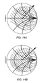
- FIG. 14A depicts load-pull contours for a PA operating at PWL 5 in a module that implements a load switch circuit according to the present disclosure.
- FIG. 14B depicts load-pull contours for a PA operating at PWL 7 in a module that implements a load switch circuit according to the present disclosure.
- a preferred embodiment of the present disclosure is incorporated in a mobile terminal 32 , such as a mobile telephone, a personal digital assistant, or the like.
- the basic architecture of the mobile terminal 32 and may include a receiver front end 34 , a radio frequency transmitter section 36 , an antenna 38 , a duplexer or switch 40 , a baseband processor 42 , a control system 44 , a frequency synthesizer 46 , and an interface 48 .
- the receiver front end 36 receives information bearing radio frequency signals from one or more remote transmitters provided by a base station.
- a low noise amplifier 50 amplifies the signal.
- a filter circuit 52 minimizes broadband interference in the received signal, while downconversion and digitization circuitry 54 downconverts the filtered, received signal to an intermediate or baseband frequency signal, which is then digitized into one or more digital streams.
- the receiver front end 34 typically uses one or more mixing frequencies generated by the frequency synthesizer 46 .
- the baseband processor 42 processes the digitized received signal to extract the information or data bits conveyed in the received signal. This processing typically comprises demodulation, decoding, and error correction operations. As such, the baseband processor 42 is generally implemented in one or more digital signal processors (DSPs).
- DSPs digital signal processors
- the baseband processor 42 receives digitized data, which may represent voice, data, or control information, from the control system 44 , which it encodes for transmission.
- the encoded data is output to the radio frequency transmitter 36 , where it is used by a modulator 56 to modulate a carrier signal that is at a desired transmit frequency.
- Power amplifier (PA) circuitry 58 amplifies the modulated carrier signal to a level appropriate for transmission from the antenna 38 .
- the amplified signal is sent to the switch 40 and antenna 38 through a switchable impedance network 60 , which is configured to set the overall load impedance for the PA circuitry 58 to optimize values based on the power level being transmitted.
- the switch 40 and antenna 38 provide a relatively constant load impedance, which is combined with the impedance of the switchable impedance network 60 to establish an overall load impedance for the PA circuitry 58 .
- a load switch control signal 62 is provided by the control system 44 to select an impedance matching network section, which will vary depending on the power level being transmitted.
- the structure and operation of impedance matching network sections comprising the switchable impedance network 60 is provided in greater detail below.
- a user may interact with the mobile terminal 32 via the interface 48 , which may include interface circuitry 64 associated with a microphone 66 , a speaker 68 , a keypad 70 , and a display 72 .
- the interface circuitry 64 typically includes analog-to-digital converters, digital-to-analog converters, amplifiers, and the like. Additionally, it may include a voice encoder/decoder, in which case it may communicate directly with the baseband processor 42 .
- the microphone 66 will typically convert audio input, such as the user's voice, into an electrical signal, which is then digitized and passed directly or indirectly to the baseband processor 42 . Audio information encoded in the received signal is recovered by the baseband processor 42 , and converted into an analog signal suitable for driving speaker 68 by the I/O and interface circuitry 64 .
- the keypad 70 and the display 72 enable the user to interact with the mobile terminal 32 , input numbers to be dialed, address book information, or the like, as well as monitor call progress information.
- FIG. 10A is a general schematic representation of a load switch circuit 74 according to the present disclosure.
- Load switch circuit 74 includes a power amplifier 76 for amplifying a radio frequency signal to provide an amplified radio frequency signal having a first power level and at least a second power level.
- a first impedance matching network section 78 is in electrical communication with the power amplifier 76 to receive the amplified radio frequency signal.
- a second impedance matching network section 80 is in electrical communication with the first impedance matching network section 78 to receive the amplified radio frequency signal, wherein the second impedance matching 80 network has an output 82 for the amplified radio frequency signal that is selectively placed in electrical communication with a load network 84 via a switch S 1 during transmission of the amplified radio frequency signal at the first power level.
- the load network 84 typically includes a harmonic filter 86 and an antenna 88 .
- a third impedance matching network section 90 is in electrical communication with the first impedance matching network section 78 to receive the amplified radio frequency signal, wherein the third impedance matching network section 90 has an output 92 for the amplified radio frequency signal that is selectively placed in electrical communication with the load network 84 via a switch S 2 during transmissions of the amplified radio frequency signal at the second power level.
- Additional impedance matching network sections such as an Nth impedance matching network section 94 is in electrical communication with the first impedance matching network section 78 , wherein the Nth impedance matching network section 94 has an output 96 that is selectively placed in electrical communication with the load network 84 via a switch SN during transmissions of the amplified radio frequency signal at an Nth power level.
- any one of the switches S 1 , S 2 and SN creates a series path for the amplified radio frequency signal through the first impedance network section 78 , and the corresponding one of the impedance matching network sections 80 , 90 , or 94 .
- the switches S 1 , S 2 and SN not only function as impedance matching network selectors, but also function as transmit and receive switches. Due to their dual function, the switches S 1 , S 2 and SN do not introduce addition energy losses relative to conventional switching circuitry used to switch impedance matching elements in conventional load switch circuits.
- the control system 44 provides the load switch control signal 62 ( FIG. 9 ) for opening and closing the switches S 1 , S 2 , S 3 and SN. In a receive mode, the control system 44 opens the switches S 1 , S 2 , and SN before closing switch S 3 . While the switch S 3 is closed, RF signals received by antenna 88 are conducted to the receiver front end 34 .
- FIG. 10B is a general schematic representation of the load switch circuit of FIG. 10A wherein the switches S 1 , S 2 , S 3 and SN are depicted as electronic switches SE 1 , SE 2 , SE 3 and SEN.
- the electronic switches SE 1 , SE 2 , SE 3 and SEN may be implemented as transistor switches as depicted in FIG. 10B .
- the transistor switches may each be a field effect transistor (FET) or other transistor type that is useable to switch radio frequency signals.
- FET field effect transistor
- the gates of the FET transistors making up switches SE 1 , SE 2 , SE 3 and SEN are each driven by the switch control signal 62 that is provided by the control system 44 .
- the switch control signal 62 turns the FET transistors either on or off.
- the FET making up the switch SE 1 when the FET making up the switch SE 1 is turned on, the output 82 of the second impedance matching network section 80 is connected to the input of the harmonic filter 86 .
- the FET making up the switch SE 1 When the FET making up the switch SE 1 is turned off, the FET will provide a high impedance or open-circuit condition that disconnects the second impedance matching network section 80 from the input of the harmonic filter 86 .
- the FETs making up SE 2 and SEN work in a similar fashion.
- the FET making up switch SE 3 will provide a high impedance or open circuit condition when the switch SE 3 is turned off. In this way, an amplified RF signal meant for transmission from the antenna 88 will be impeded from being received by the receiver front end 34 .
- the switch SE 3 when the switch SE 3 is turned on a low impedance path for RF signals received by the antenna 88 is provided between the receiver front end 34 and the receiver front end 34 .
- FIG. 11 is a detailed schematic of an embodiment of a load switch circuit 98 according to the present disclosure.
- Load switch circuit 98 is useable to increase the PAE of a power amplifier (PA) 100 that is operable at ECTEL power levels PWL 5 and PWL 7 .
- a first impedance matching network section 102 comprises a traditional L-C-L-C-L circuit with inductive components L 1 , L 2 and L 3 , and capacitive components C 1 and C 2 .
- a first terminal of L 1 is coupled to an output 104 of the PA 100 in order to receive an amplified radio frequency signal from the PA 100 .
- a second terminal of L 1 is coupled to a first terminal of L 2 and a first terminal of C 1 at a common node 106 .
- a second terminal of C 1 is coupled to a ground node 108 .
- a second terminal of L 2 is coupled to a first terminal of L 3 and a first terminal of C 2 at a common node 110 .
- a second terminal of C 2 is coupled to the ground node 108 .
- a second terminal of L 3 is an output node 112 for the first impedance matching network section 102 .
- a second impedance matching network section 114 has an inductor L 4 , and capacitors C 4 and C 5 .
- a first terminal of L 4 is coupled to the second terminal of L 3 at the output node 112 .
- a second terminal L 4 is coupled to a first terminal of C 4 and a first terminal of C 5 at a common node 116 .
- a second terminal of C 4 is coupled to the ground node 108 .
- a second terminal of C 5 is an output node 118 for the second impedance matching network section 114 .
- a third impedance network section 120 has capacitors C 3 and C 6 , and an inductor L 5 .
- a first terminal of C 3 is coupled to the second terminal of L 3 , and the first terminal of L 4 at the output node 112 .
- a second terminal of C 3 is coupled to a first terminal of C 6 and a first terminal of L 5 at a common node 122 .
- a second terminal of C 6 is coupled to the ground node 108 .
- a second terminal of L 5 is an output node 124 for the third impedance network section 120 .
- An load network 126 is comprised of a harmonic filter 128 and an antenna 130 .
- An output terminal of the harmonic filter 128 is coupled to an input of the antenna 130 .
- a switch S 1 for selectively coupling the second impedance matching network section 114 has a first terminal that is coupled to the output node 118 .
- a second terminal of switch S 1 is coupled to an input terminal of the harmonic filter 128 at a common node 132 .
- a switch S 2 for selectively coupling the third impedance matching network section 120 has a first terminal that is coupled to the output node 124 .
- a second terminal of switch S 2 is coupled to the input terminal of the harmonic filter 128 at the common node 132 .
- FIG. 12 is a schematic representing the operation of the load switch circuit 98 at ECTEL power level PWL 7 . While operating at the PWL 7 power level, the switch S 1 is closed and the switch S 2 is left open. As a result of the switch S 2 being open, the inductor L 5 does not present an impedance matching effect. Thus, L 5 is not shown as part of an equivalent circuit section 134 . However, as shown in the equivalent circuit section 134 , the capacitors C 3 and C 5 are placed in series.
- Capacitors C 3 and C 6 function as a total capacitive reactance incorporated in the matching network.
- FIG. 13 is a schematic representing the operation of the load switch circuit 98 at ECTEL power level PWL 5 .
- the switch S 2 is closed and the switch S 1 is left open.
- the capacitor C 5 does not present an impedance matching effect.
- C 5 is not shown as part of an equivalent circuit section 136 , which places inductor L 4 in series with capacitor C 4 .
- the inductor L 4 and the capacitor C 4 may be selected such that a resonant frequency for the equivalent circuit section 136 is above the carrier frequency of a radio frequency being amplified by PA 100 . In this way, the equivalent circuit section 136 behaves as a capacitive reactance at the carrier frequency of radio frequency being passed to the load network 126 .
- component values for the inductors L 1 -L 5 , and C 1 -C 6 be selected such that a collector impedance of PA 100 in the approximate range of 7-7.5 Ohms is matched by the first and second impedance matching networks sections 102 and 114 for PWL 7 operation.
- component values for the inductors L 1 -L 5 , and C 1 -C 6 be selected such that a collector impedance of approximately 2.5 Ohms is matched by the first and third impedance network sections 102 and 120 for PWL 5 operation.
- a sweetspot for operating the PA 100 at the PWL 5 power level may be rotated on a Smith Chart to an optimum angle via C 5 and L 5 without affecting an optimum impedance match for the PWL 7 power level. Therefore, an advantage of the load switch circuit 98 is that the alignment of the sweetspots for operation at both the PWL 5 and PWL 7 power levels is realizable.
- FIGS. 14A and 14B depict load-pull contours for a PA in a module that implements the load switch circuit 98 ( FIGS. 12 , 13 and 14 ).
- the load-pull contours of FIG. 14A are for PA 100 operated at the PWL 5 power level.
- the load-pull contours of FIG. 14B are for PA 100 operated at the PWL 7 power level. Notice that the sweetspots for both the PWL 5 and PWL 7 power levels are in the upper right quadrants of a series of PA output current contours shown overlaying a Smith chart for both FIGS. 14A and 14B .
- a load impedance for load network 84 is represented by load impedance arrows that extend from the centers of the Smith Charts. As a result, of the method and system of the present disclosure, the load impedance arrows are rotated and aligned into the regions where the PA 100 has minimum current draw in both power levels PWL 5 and PWL 7 .
- the electronic switches SE 1 , SE 2 , SE 3 , and SEN in FIG. 10B may also be implemented using a diode with a diode switching network.
- the diode may be of the positive-intrinsic-negative (PIN) diode type or other type that is useable to switch radio frequency signals. All such improvements and modifications are considered within the scope of the concepts disclosed herein and the claims that follow.
Landscapes
- Transmitters (AREA)
- Amplifiers (AREA)
Abstract
Description
-
- The impedance presented to the collector of the PA's output transistor. This impedance needs to be designed such that the PA can provide a desired output power, but no more than the desired output power.
- The minimization of energy losses due to the output impedance matching network.
- The harmonic termination seen from the collector of the PA's output transistor, which is to a large degree associated with the class of the PA (i.e., class AB, F, E, and so on).
A well designed load switch circuit with an output impedance matching network ensures that all three criteria are met. Unfortunately, designing a load switch circuit with an output impedance matching network needed to provide a desired output power, but no more than the desired output power while minimizing energy losses due to the output impedance matching network is a particularly difficult challenge.
-
- The output impedance matching network must be able to present optimized antenna impedance to the PA's collector for both
power levels PWL 5 andPWL 7. - The energy loss due to the output impedance matching network must be low for both power levels whether the output impedance matching network is designed for a fifty Ohm antenna load or other antenna impedances located within a VSWR circle. Therefore, it is preferred that the load impedance arrow representing antenna impedance be rotated to the sweetspot for electrical current contours on the Smith Chart.
- The harmonics must be properly terminated in
power levels PWL 5 andPWL 7. - The sweetspot must be aligned such that the load impedance arrow may be rotated into the region where the PA has minimum current draw in
power levels PWL 5 andPWL 7.
- The output impedance matching network must be able to present optimized antenna impedance to the PA's collector for both
-
- The component that is switched into the output matching network exhibits a poor quality factor (Q-factor) because of the loss coming from the switch. A poor Q-factor may be avoided by using Micro-electromechanical Systems (MEMS) devices. However, MEMS devices are expensive and often require additional circuitry. The poor Q-factor of a component switched into an impedance matching network results in a high energy loss for the impedance matching network, which results in a degraded PAE.
- Since the sweetspots of the
PWL 5 andPWL 7 match are not well aligned, it is not possible to rotate the load impedance arrow to an optimum angle for both power levels. However, this deficiency can be solved by using more than a single load switch such that multiple components are switched at a time. In general, having multiple load switches in an output impedance matching network is not a desirable solution because any additional switches will increase the energy loss, which reduces PAE. Further still, multiple load switches and associated components add financial cost to manufacturing a mobile terminal circuit board.
Claims (23)
Priority Applications (1)
| Application Number | Priority Date | Filing Date | Title |
|---|---|---|---|
| US12/835,793 US8437714B1 (en) | 2009-07-14 | 2010-07-14 | Advanced load-switch circuit with zero phase rotation |
Applications Claiming Priority (4)
| Application Number | Priority Date | Filing Date | Title |
|---|---|---|---|
| US22544109P | 2009-07-14 | 2009-07-14 | |
| US24338709P | 2009-09-17 | 2009-09-17 | |
| US30178910P | 2010-02-05 | 2010-02-05 | |
| US12/835,793 US8437714B1 (en) | 2009-07-14 | 2010-07-14 | Advanced load-switch circuit with zero phase rotation |
Publications (1)
| Publication Number | Publication Date |
|---|---|
| US8437714B1 true US8437714B1 (en) | 2013-05-07 |
Family
ID=48183310
Family Applications (1)
| Application Number | Title | Priority Date | Filing Date |
|---|---|---|---|
| US12/835,793 Active 2031-07-25 US8437714B1 (en) | 2009-07-14 | 2010-07-14 | Advanced load-switch circuit with zero phase rotation |
Country Status (1)
| Country | Link |
|---|---|
| US (1) | US8437714B1 (en) |
Citations (2)
| Publication number | Priority date | Publication date | Assignee | Title |
|---|---|---|---|---|
| US20090174496A1 (en) * | 2006-07-12 | 2009-07-09 | Adrianus Van Bezooijen | Load-Line Adaptation |
| US20100056089A1 (en) * | 2008-08-29 | 2010-03-04 | Shahram Tadayon | Mechanical tuning of a radio |
-
2010
- 2010-07-14 US US12/835,793 patent/US8437714B1/en active Active
Patent Citations (2)
| Publication number | Priority date | Publication date | Assignee | Title |
|---|---|---|---|---|
| US20090174496A1 (en) * | 2006-07-12 | 2009-07-09 | Adrianus Van Bezooijen | Load-Line Adaptation |
| US20100056089A1 (en) * | 2008-08-29 | 2010-03-04 | Shahram Tadayon | Mechanical tuning of a radio |
Non-Patent Citations (5)
| Title |
|---|
| "Battery Life Testing Application Notes-rev. 1.1," Racal 6103 Digital Radio Test Set Product Information Sheet, copyright 1998, pp. 1-4, Racal Instruments Limited. |
| De Graauw, A.J.M. et al., "MEMS-Based Reconfigurable Multi-band BiCMOS Power Amplifier," 2006 Bipolar/ BiCMOS Circuits and Technology Meeting, Oct. 8-10, 2006, pp. 1-4, IEEE. |
| Jeong, Hyeong Tae et al., "Efficiency enhancement method for high-power amplifiers using a dynamic load adaptation technique," 2005 IEEE MTT-S International Microwave Symposium Digest, Jun. 12-17, 2005, pp. 2059-2062, IEEE. |
| Larcher, L. et al., "A MEMS reconfigurable quad-band Class-E Power Amplifier for GSM standard," 2009 Design, Automation & Test in Europe Conference & Exhibition, Apr. 20-24, 2009, pp. 364-368, IEEE. |
| Zhang, Chunna et al., "A novel reconfigurable power amplifier structure for multi-band and multi-mode portable wireless applications using a reconfigurable die and a switchable output matching network," 2009 IEEE MTT-S International Microwave Symposium Digest, Jun. 7-12, 2009, pp. 913-916, IEEE. |
Similar Documents
| Publication | Publication Date | Title |
|---|---|---|
| US6384688B1 (en) | High-frequency power amplifier module | |
| US11082008B2 (en) | Multi-mode stacked amplifier | |
| US6819941B2 (en) | Single output stage power amplification for multimode applications | |
| US6515541B2 (en) | Multi-level power amplifier | |
| US7053706B2 (en) | High linearity doherty communication amplifier with bias control | |
| CN104682884B (en) | Device and method for the phase compensation in power amplifier | |
| US6970040B1 (en) | Multi-mode/multi-band power amplifier | |
| EP0687060B1 (en) | Power amplifier | |
| US9203362B2 (en) | Quadrature lattice matching network | |
| US7493094B2 (en) | Multi-mode power amplifier module for wireless communication devices | |
| US20040121745A1 (en) | Method and apparatus for impedance matching in an amplifier using lumped and distributed inductance | |
| US20140327483A1 (en) | Complementary metal oxide semiconductor power amplifier | |
| KR20010053413A (en) | Mobile telephone system | |
| KR100470582B1 (en) | Method and apparatus for multiple band transmission | |
| WO1997013320A1 (en) | Power amplifier and communication device | |
| US6680652B2 (en) | Load switching for transmissions with different peak-to-average power ratios | |
| US6466770B1 (en) | BALUN circuit for combining differential power amplifier outputs | |
| EP0987826A2 (en) | Radio transceiver switching circuit | |
| US6711392B1 (en) | Balanced power amplifier for low power radio communications | |
| CN213879763U (en) | Power amplifying circuit | |
| US8437714B1 (en) | Advanced load-switch circuit with zero phase rotation | |
| JP2002016448A (en) | Radio frequency amplifier circuit and receiving chain circuit | |
| EP1054507A2 (en) | Mobile station employing single ended use of a differential power amplifier for reduced output power | |
| KR100514679B1 (en) | RF terminal module structure of mobile communication terminal | |
| KR101034106B1 (en) | Complex Module Impedance Regulator |
Legal Events
| Date | Code | Title | Description |
|---|---|---|---|
| AS | Assignment |
Owner name: RF MICRO DEVICES, INC., NORTH CAROLINA Free format text: ASSIGNMENT OF ASSIGNORS INTEREST;ASSIGNORS:UBBESEN, LARS SANDAHL;NIELSEN, MICHAEL;SIGNING DATES FROM 20100709 TO 20100712;REEL/FRAME:024680/0327 |
|
| AS | Assignment |
Owner name: BANK OF AMERICA, N.A., AS ADMINISTRATIVE AGENT, TE Free format text: NOTICE OF GRANT OF SECURITY INTEREST IN PATENTS;ASSIGNOR:RF MICRO DEVICES, INC.;REEL/FRAME:030045/0831 Effective date: 20130319 |
|
| STCF | Information on status: patent grant |
Free format text: PATENTED CASE |
|
| AS | Assignment |
Owner name: RF MICRO DEVICES, INC., NORTH CAROLINA Free format text: TERMINATION AND RELEASE OF SECURITY INTEREST IN PATENTS (RECORDED 3/19/13 AT REEL/FRAME 030045/0831);ASSIGNOR:BANK OF AMERICA, N.A., AS ADMINISTRATIVE AGENT;REEL/FRAME:035334/0363 Effective date: 20150326 |
|
| AS | Assignment |
Owner name: QORVO US, INC., NORTH CAROLINA Free format text: MERGER;ASSIGNOR:RF MICRO DEVICES, INC.;REEL/FRAME:039196/0941 Effective date: 20160330 |
|
| REMI | Maintenance fee reminder mailed | ||
| FPAY | Fee payment |
Year of fee payment: 4 |
|
| SULP | Surcharge for late payment | ||
| MAFP | Maintenance fee payment |
Free format text: PAYMENT OF MAINTENANCE FEE, 8TH YEAR, LARGE ENTITY (ORIGINAL EVENT CODE: M1552); ENTITY STATUS OF PATENT OWNER: LARGE ENTITY Year of fee payment: 8 |
|
| MAFP | Maintenance fee payment |
Free format text: PAYMENT OF MAINTENANCE FEE, 12TH YEAR, LARGE ENTITY (ORIGINAL EVENT CODE: M1553); ENTITY STATUS OF PATENT OWNER: LARGE ENTITY Year of fee payment: 12 |