US8427252B2 - Oscillators with low power mode of operation - Google Patents
Oscillators with low power mode of operation Download PDFInfo
- Publication number
- US8427252B2 US8427252B2 US13/149,662 US201113149662A US8427252B2 US 8427252 B2 US8427252 B2 US 8427252B2 US 201113149662 A US201113149662 A US 201113149662A US 8427252 B2 US8427252 B2 US 8427252B2
- Authority
- US
- United States
- Prior art keywords
- oscillator
- signal
- circuit
- low power
- enable signals
- Prior art date
- Legal status (The legal status is an assumption and is not a legal conclusion. Google has not performed a legal analysis and makes no representation as to the accuracy of the status listed.)
- Active, expires
Links
- 238000000034 method Methods 0.000 claims abstract description 11
- 230000001360 synchronised effect Effects 0.000 claims description 27
- 230000004044 response Effects 0.000 claims description 22
- 230000000295 complement effect Effects 0.000 claims description 3
- 238000010586 diagram Methods 0.000 description 33
- 239000000872 buffer Substances 0.000 description 23
- 230000007704 transition Effects 0.000 description 12
- 239000013078 crystal Substances 0.000 description 11
- 230000003111 delayed effect Effects 0.000 description 6
- 230000010355 oscillation Effects 0.000 description 6
- 230000009467 reduction Effects 0.000 description 5
- 230000001934 delay Effects 0.000 description 4
- 239000004065 semiconductor Substances 0.000 description 3
- 230000003213 activating effect Effects 0.000 description 2
- 230000002411 adverse Effects 0.000 description 2
- 238000004891 communication Methods 0.000 description 2
- 238000005516 engineering process Methods 0.000 description 2
- 230000008569 process Effects 0.000 description 2
- 230000000630 rising effect Effects 0.000 description 2
- 101000994667 Homo sapiens Potassium voltage-gated channel subfamily KQT member 2 Proteins 0.000 description 1
- 102100034354 Potassium voltage-gated channel subfamily KQT member 2 Human genes 0.000 description 1
- 101100057245 Saccharomyces cerevisiae (strain ATCC 204508 / S288c) ENA1 gene Proteins 0.000 description 1
- 101100057246 Saccharomyces cerevisiae (strain ATCC 204508 / S288c) ENA2 gene Proteins 0.000 description 1
- 230000008859 change Effects 0.000 description 1
- 230000000694 effects Effects 0.000 description 1
- 230000007246 mechanism Effects 0.000 description 1
- 229910044991 metal oxide Inorganic materials 0.000 description 1
- 150000004706 metal oxides Chemical class 0.000 description 1
- 230000004048 modification Effects 0.000 description 1
- 238000012986 modification Methods 0.000 description 1
Images


Classifications
-
- H—ELECTRICITY
- H03—ELECTRONIC CIRCUITRY
- H03B—GENERATION OF OSCILLATIONS, DIRECTLY OR BY FREQUENCY-CHANGING, BY CIRCUITS EMPLOYING ACTIVE ELEMENTS WHICH OPERATE IN A NON-SWITCHING MANNER; GENERATION OF NOISE BY SUCH CIRCUITS
- H03B5/00—Generation of oscillations using amplifier with regenerative feedback from output to input
- H03B5/30—Generation of oscillations using amplifier with regenerative feedback from output to input with frequency-determining element being electromechanical resonator
-
- H—ELECTRICITY
- H03—ELECTRONIC CIRCUITRY
- H03B—GENERATION OF OSCILLATIONS, DIRECTLY OR BY FREQUENCY-CHANGING, BY CIRCUITS EMPLOYING ACTIVE ELEMENTS WHICH OPERATE IN A NON-SWITCHING MANNER; GENERATION OF NOISE BY SUCH CIRCUITS
- H03B2200/00—Indexing scheme relating to details of oscillators covered by H03B
- H03B2200/006—Functional aspects of oscillators
- H03B2200/0082—Lowering the supply voltage and saving power
Definitions
- the present embodiments relate generally to oscillator circuitry and specifically relate to oscillators with a low power mode of operation.
- Timing of various components of a computer system is synchronized by clock signals generated by oscillator circuits.
- conventional mother boards of personal computers include a real time clock (RTC) and a crystal oscillator circuit to provide the main clock for mother board components such as input/output (I/O) controllers.
- Clock signals are also essential in numerous other electronic systems and devices that process digital signals. Radio communication systems and devices use oscillator circuits as an indispensible part of their modulation and demodulation circuitries to generate sinusoidal signals.
- high-accuracy, high-speed clock signals are required. For example, network devices need to maintain high-accuracy timers even when operating in a low power mode.
- generating high-accuracy oscillators that generate high-speed clock signals can consume significant amounts of power.
- oscillator circuits generating oscillations with precise frequencies use a crystal as an oscillator core to govern their resonating signals.
- a gain element such as a transistor can be used to amplify the resonating signal and feed it back to the oscillator core.
- the conventional crystal oscillator 100 of FIG. 1 uses a transistor M 1 as the gain element.
- the core of oscillator 100 is a crystal 110 connected in parallel with a resistor 120 .
- a current source 130 connected between a power supply Vcc and a drain of the transistor M 1 at an output node 140 , provides a bias current for the transistor M 1 .
- the resistor 120 connected between a gate of the transistor M 1 and an output node 140 of the conventional crystal oscillator 100 , provides a negative feedback between the drain and the gate of the transistor M 1 , which in turn ensures a stable DC operating point of the conventional crystal oscillator 100 .
- a circuit 150 may use a clock signal CLK generated at the output node 140 , for instance, to synchronize timing of its various components.
- the current source 130 of the conventional crystal oscillator 100 is always ON and there is no provision for lowering a power level of the crystal oscillator 100 for time periods that the circuit 150 is fully or partially in an inactive (e.g., sleep) mode. Consequently, the conventional crystal oscillator 100 may be impractical in applications for which lower power consumption is increasingly important.
- a circuit 200 of FIG. 2 illustrates a conventional solution that includes a main oscillator 210 , an LPO 220 , and a multiplexer (MUX) 230 .
- the MUX 230 selectively connects either the main oscillator 210 or the LPO 220 to a circuit CKT 240 in response to the select signal SEL.
- the select signal SEL is driven to a first state that allows the main oscillator 210 to provide clock signals to the circuit CKT 240 , and during a low power mode, the select signal SEL is driven to a second state that allows the LPO 220 to provide clock signals to the circuit CKT 240 .
- FIG. 1 is a schematic diagram of a conventional oscillator circuit
- FIG. 2 is a schematic diagram of a conventional oscillator circuit including a main oscillator and an LPO;
- FIG. 3 is a block diagram of an oscillator circuit in accordance with some embodiments.
- FIG. 4 is a functional diagram of a state machine providing enable signals for the oscillator circuit of FIG. 3 in accordance with some embodiments;
- FIG. 5A depicts a timing diagram of a set of enable signal waveforms generated by the state machine of FIG. 4 in accordance with some embodiments
- FIG. 5B depicts a timing diagram of another set of enable signal waveforms generated by the state machine of FIG. 4 in accordance with some embodiments
- FIG. 6 is a schematic diagram of an exemplary embodiment of the oscillator circuit of FIG. 3 ;
- FIG. 7 is a schematic diagram of an exemplary embodiment of a portion of a gain circuit of the oscillator circuit of FIG. 6 ;
- FIG. 8 is a functional block diagram of an exemplary embodiment of the state machine of FIG. 4 ;
- FIG. 9 is a schematic diagram of an exemplary embodiment of the synchronizer circuit of FIG. 8 ;
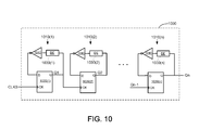
- FIG. 10 is a schematic diagram of an exemplary embodiment of the counter circuit of FIG. 8 ;
- FIG. 11 is a schematic diagram of an exemplary embodiment of the duty cycle control circuit of FIG. 8 ;
- FIG. 12 is a timing diagram of signals generated by the circuits of FIGS. 10 and 11 ;
- FIG. 13 is a schematic diagram of exemplary embodiment of the enable signal control circuit of FIG. 8 ;
- FIG. 14 is a schematic diagram of a glitch reduction circuit for the oscillator circuit of FIG. 6 in accordance with some embodiments.
- FIG. 15 is a timing diagram of exemplary signals generated by the circuit of FIG. 14 ;
- FIG. 16 is a flow chart illustrating a method for reducing the operational power level in oscillator circuits in accordance with some embodiments.
- a method and apparatus for generating clock signals using oscillator circuits having a low power mode of operation are disclosed.
- numerous specific details are set forth such as examples of specific components, circuits, and processes to provide a thorough understanding of the present disclosure.
- specific nomenclature is set forth to provide a thorough understanding of the present embodiments.
- well-known circuits and devices are shown in block diagram form to avoid obscuring the present disclosure.
- the term “coupled” as used herein means connected directly to or connected through one or more intervening components or circuits.
- any of the signals provided over various buses described herein may be time-multiplexed with other signals and provided over one or more common buses.
- the interconnection between circuit elements or software blocks may be shown as buses or as single signal lines.
- Each of the buses may alternatively be a single signal line, and each of the single signal lines may alternatively be buses, and a single line or bus might represent any one or more of myriad physical or logical mechanisms for communication between components.
- the logic levels assigned to various signals in the description below are arbitrary, and therefore may be modified (e.g., reversed polarity) as desired.
- circuits described or depicted as including metal oxide semiconductor (MOS) transistors may alternatively be implemented using bipolar transistors or any other technology in which a signal-controlled current flow may be achieved.
- MOS metal oxide semiconductor
- signals referred to herein as clock signals may alternatively be strobe signals or any other signals that provide timing control. Accordingly, the present embodiments are not to be construed as limited to specific examples described herein but rather includes within its scope all embodiments defined by the appended claims.
- An oscillator circuit in accordance with present embodiments is configured to selectively switch between a low power mode and a normal mode of operation.
- the oscillator circuit includes an oscillator core that includes an oscillation generator in parallel with a gain circuit.
- the oscillator core is configured to generate clock signals.
- One or more elements of the gain circuit can be selectively disabled to reduce the operating power level of the oscillator circuit (e.g., during the low power mode) without adversely affecting accuracy of generated clock signals.
- the oscillator circuit is embedded in an integrated circuit of a semiconductor chip, which may at times enter into a sleep mode.
- the oscillator circuit can be dynamically switched to a low power mode of operation.
- the oscillator circuit can enter into the low power mode of operation even when the chip is not in the sleep mode.
- a low power mode signal may trigger a state machine to generate enable signals that can disable selected portions of the gain circuit to reduce the operational power of the oscillator circuit.
- FIG. 3 is a block diagram of an oscillator circuit 300 in accordance with some embodiments.
- An oscillator core 310 is connected in parallel with a dynamically configurable gain circuit 320 .
- the oscillator core 310 which is well-known, generates electrical oscillations that ultimately produce clock signals at terminals Xin and Xout.
- the dynamically configurable gain circuit 320 includes a plurality of gain elements G 1 -Gn selectively connected in parallel with the oscillator core 310 .
- the gain elements G 1 -Gn are selectively enabled and disabled by respective enable signals EN 1 -ENn. For example, enable signal EN 2 selectively enables and disables gain element G 2 to be operational.
- the gain elements G 1 -Gn When enabled, the gain elements G 1 -Gn provide a gain for the oscillator core 310 . When a gain element is disabled, the gain element does not conduct current between the supply voltage and ground potential, and therefore does not provide a gain for the oscillator core 310 and, perhaps more importantly for present embodiments, consumes minimal (if any) power.
- the enable signals may be generated by any suitable circuit, logic, and/or processor.
- selectively disabling one or more of the gain elements G 1 -Gn advantageously lowers the operational power of the oscillator circuit 300 during the low power mode.
- the gain elements G 1 -Gn may provide a fraction of their normal gain to the oscillator core 310 during the low power mode, for example, by intermittingly pulsing their corresponding enable signals to an asserted state such that the gain elements are enabled only during brief time intervals (e.g., and disabled for longer time intervals).
- the gain circuit 320 can provide a minimal gain to the oscillator core 310 to ensure that the oscillator core 310 is able to continue generating the clock signal during the low power mode, while also significantly reducing power consumption by not drawing current during the longer time intervals during which the gain elements are disabled.
- oscillator circuit 300 may include one or more additional gain elements (not shown in FIG. 3 for simplicity) that remain in continuous operation during the low power mode.
- FIG. 4 is a functional diagram of a state machine 400 providing enable signals EN 1 -ENn for the oscillator circuit 300 of FIG. 3 in accordance with some embodiments.
- the state machine 400 receives a clock signal CLK 0 and a mode select signal MODE_SEL, and generates the enable signals EN 1 -ENn in response thereto.
- the clock signal CLK 0 is derived from an output of the oscillator circuit 300 , and for some embodiments is synchronized with the mode select signal MODE_SEL as described below with respect to FIG. 9 .
- the mode select signal MODE_SEL is used to indicate a mode of operation of the oscillator circuit 300 .
- the mode select signal MODE_SEL is driven to a first state to select a normal mode of operation, and is driven to a second state to select a low power mode of operation. More specifically, when MODE — SEL is driven to the first state to select the normal mode of operation, a number of the enable signals EN 1 -ENn are asserted to enable all corresponding gain elements G 1 -Gn, thereby allowing oscillator circuit 300 to operate in a normal manner (e.g., with enough gain to attain acceptable performance).
- the enable signals EN 1 -ENn are selectively asserted to selectively disable one or more of the corresponding gain elements G 1 -Gn, thereby allowing oscillator circuit 300 maintain its clock generation function while significantly reducing power consumption.
- the present embodiments allow for a significant reduction in power consumption for oscillator circuits (e.g., during low power mode) without employing a separate low-power oscillator circuit.
- FIG. 5A depicts a timing diagram 500 A illustrating an exemplary set of enable signal waveforms 510 ( 1 )- 510 ( n ) generated by the state machine 400 of FIG. 4 during the normal operational mode.
- the enable signal waveforms 510 ( 1 )- 510 ( n ), which correspond to the respective enable signals En 1 -ENn, are continually asserted to enable a number of the gain elements G 1 -Gn to provide continuous gain for the oscillator core 310 during the normal mode of operation.
- FIG. 5B depicts a timing diagram 500 B illustrating an exemplary set of enable signal waveforms 520 ( 1 )- 520 ( n ) generated by the state machine 400 of FIG. 4 during the low power mode.
- the state machine 400 selectively asserts the enable signals EN 1 -ENn for brief intervals or pulses, which in turn temporarily enables corresponding gain elements G 1 -Gn of the dynamically configurable gain circuit of FIG. 3 .
- the corresponding gain elements G 1 -Gn are disabled, and therefore do not provide gain for the oscillator core 310 and, perhaps more importantly, consume little, if any, power.
- enable signals EN 1 -ENn may be sequentially staggered by time delays, for example, as described in more detail below with respect to FIG. 13 .
- the staggered assertion of the enable signals precludes adverse effects on the clocks generated by the oscillator circuit 300 of FIG. 3 resulting from abrupt changes in gain of the gain circuit 320 of the oscillator circuit 300 .
- operation of the oscillator circuit 300 with zero delay times between enable signals EN 1 -ENn may be acceptable.
- FIG. 6 is a schematic diagram of an oscillator 600 that is one embodiment of the oscillator circuit 300 of FIG. 3 .
- the oscillator circuit 600 includes the oscillator core 310 connected in parallel with the gain circuit 320 .
- the oscillator core 310 includes a crystal 620 connected in parallel with a resistor 610 .
- the gain circuit 320 includes a number of selectable gain elements 650 ( 1 )- 650 ( n ), each of which includes a corresponding one of gain elements G 1 -Gn selectively connected between Vcc and ground potential by a corresponding pair of switches SA and SB, respectively, in response to an associated one of the enable signals EN 1 -ENn.
- each of the gain elements G 1 -Gn can be selectively enabled and disabled by activating the respective pairs of switches SA 1 -SAn and SB 1 -SBn in response to corresponding enable signals EN 1 -ENn, as depicted in FIG. 6 .
- switches SA 2 and SB 2 selectively connect gain element G 2 between Vcc and ground potential in response to enable signal EN 2 .
- each enable signal EN is formed by a pair of complemented enable signals (e.g., ENA and ENB) that are provided to control terminals of the corresponding pair of switches SA and SB, for example, as described in more detail below with respect to FIG. 7 .
- gain circuit 320 is shown to include an additional gain element G 0 connected directly between Vcc and ground potential without any switches. In this manner, gain element G 0 is continuously enabled to provide an uninterrupted gain that sustains oscillations of the oscillator core 310 .
- any number of gain elements may be connected between Vcc and ground potential without switches.
- the gain elements G 0 -Gn and the corresponding switches SA and SB can be implemented in various ways, for example, by using CMOS technology.
- FIG. 7 is a schematic diagram of a selectable gain element 700 that is one embodiment of the selectable gain element 650 of FIG. 6 .
- the selectable gain element 700 includes a first PMOS transistor MP 1 , a second PMOS transistor MP 2 , a first NMOS transistor MN 1 , and a second NMOS transistor MN 2 .
- PMOS transistor MP 2 and NMOS transistor MN 2 form gain element G of FIG. 6 .
- Gate terminals of the PMOS transistor MP 2 and the NMOS transistor MN 2 are connected together to form an input node (Xin) of the gain element G, and drain terminals of PMOS transistor MP 2 and NMOS transistor MN 2 are connected together to form an output node (Xout) of the gain element G 2 .
- connections to the power supply Vcc and ground potential for PMOS transistor MP 2 and NMOS transistor MN 2 are provided by the PMOS transistor MP 1 and the NMOS transistor MN 1 , which operate as switches S 2 A and S 2 B of FIG. 6 , respectively.
- a source terminal of the PMOS transistor MP 1 is connected to Vcc, while its drain terminal is connected to a source terminal of the PMOS transistor MP 2 .
- Bodies of PMOS transistors MP 1 and MP 2 are jointly connected to the source of PMOS transistor MP 1 .
- a source terminal of NMOS transistor MN 1 is connected to ground potential and its drain terminal is connected to a source terminal of NMOS transistor MN 2 .
- Bodies of the NMOS transistors MN 1 and MN 2 are connected together and to the source of NMOS transistor MN 1 .
- Gate terminals of PMOS transistor MP 1 and NMOS transistor MN 1 operate as activating terminals of the switches SA and SB, respectively, of FIG. 6 .
- Asserting enable signal ENB to logic high turns on NMOS transistor MN 1
- asserting enable signal ENA to logic low turns on PMOS transistor MP 1 , thereby enabling the gain element by connecting the gain element to power sources Vcc and ground potential.
- the enable signals are generated by the state machine 400 of FIG. 4 , an exemplary embodiment of which is described in more detail below with respect to FIG. 8 .
- FIG. 8 is a functional block diagram of a state machine 800 that is one embodiment of the state machine 400 of FIG. 4 .
- the state machine 800 includes a synchronizer circuit 810 , a counter circuit 820 , a duty cycle control circuit 830 , and an enable signal control circuit 840 .
- the state machine 800 receives clock signal CLK 0 and mode select signal MODE_SEL, and in response thereto generates the enable signals EN 1 -ENn.
- the clock signal CLK 0 which is derived from the output Xout of the oscillator circuit 600 , is synchronized with mode select signal MODE_SEL by the synchronizer circuit 810 to generate a synchronized clock signal CLKS.
- the synchronized clock signal CLKS is used by the counter circuit 820 to provide one cycle of an output count signal Qn per each k (e.g., 8) cycles of the synchronized clock signal CLKS.
- the output count signal Qn is provided to the duty cycle control circuit 830 , which in turn modifies the duty cycle of the output count signal Qn to generate an oscillator control signal OSCN.
- the oscillator control signal OSCN drives the enable signal control circuit 840 , which generates the enable signals EN 1 -ENn for controlling the gain elements G 1 -Gn of the gain circuit 320 of FIG. 6 .
- the state machine 800 is shown in FIG. 8 to include hardware including various circuits, in some embodiments, its functionalities may be performed by software and/or firmware or by a combination of hardware and software and/or firmware.
- FIG. 9 is a schematic diagram of a synchronizer circuit 900 that is one embodiment of the synchronizer circuit 810 of FIG. 8 .
- the synchronizer circuit 900 is shown to include a buffer 910 , a flip-flop 920 , and a NAND gate 930 .
- the buffer 910 is a CMOS inverter, as depicted in FIG. 9 .
- the synchronizer circuit 900 receives the clock signal CLK 0 derived from the output signal at node Xout of the oscillator circuit 600 of FIG. 6 , and synchronizes the clock signal CLK 0 with the mode select signal MODE_SEL to generate the synchronized clock signal CLKS.
- the clock signal CLK 0 is fed through the buffer 910 to a clock input of the flip-flop 920 , which also receives the mode select signal MODE_SEL as its data (D) input.
- the Q output of the flip-flop 920 is coupled to a first input of NAND gate 930 , which includes a second input to receive CLK 0 and includes an output to generate the synchronized clock signal CLKS. In this manner, the NAND gate 930 selectively allows the clock signal CLKS to toggle in response to MODE_SEL.
- the synchronized clock signal CLKS toggles at the same frequency as the clock signal CLK 0 .
- the synchronized clock signal CLKS runs only while MODE_SEL is asserted to a logic high state (e.g., to indicate the normal operational mode).
- MODE_SEL is de-asserted to logic low (e.g., to indicate the low power mode)
- the synchronized clock signal CKLS no longer toggles.
- the functions performed by synchronizer circuit 900 can be performed by other suitable circuitry.
- FIG. 10 is a schematic diagram of a counter circuit 1000 that is one embodiment of the counter circuit 820 of FIG. 8 .
- the counter circuit 1000 which includes n single-bit counter stages 1010 ( 1 )- 1010 ( n ), generates one cycle of the output count signal Qn for each 2 n cycles of input synchronized clock signal CLKS.
- Each counter stage 1010 includes a flip-flop 1020 , a delay element 1030 , and a buffer 1040 .
- the buffers 1040 are CMOS inverters, as depicted in FIG. 10 .
- the Q output of the flip-flop 1020 in each counter stage 1010 is connected to the delay element 1030 in the counter stage 1010 and to a clock input of the flip-flop 1020 in the subsequent counter stage 1010 .
- the output of the delay element 1030 is coupled to the buffer 1040 , which in turn is coupled to the D input of the corresponding flip-flop 1020 .
- the first counter stage 1010 ( 1 ) receives the synchronized clock signal CLKS at its clock input.
- Each of the counter stages 1010 ( 1 )- 1010 ( n ) divides the frequency of the clock signal provided to its clock input by a factor of two. In this manner, the counter circuit 1000 divides the frequency of the synchronized clock signal CLKS by 2 n .
- the counter circuit 1000 generates one pulse in the output count signal Qn for each 2 n cycles of the synchronized clock signal CLKS, as described in more detail below with respect to FIG. 12 . Further, it is noted that the functions performed by the counter circuit 1000 can be performed by other suitable circuitry.
- FIG. 11 is a schematic diagram of a duty cycle control circuit 1100 that is one embodiment of the duty cycle control circuit 830 of FIG. 8 .
- the duty cycle control circuit 1100 modifies the duty cycle of the output count signal Qn of the counter circuit 820 to generate the oscillator control signal OSCN.
- the duty cycle control circuit 1100 includes flip-flops 1101 - 1103 , and also includes a NOR gate 1110 .
- the signal Qn is provided to the D input of flip-flop 1101 and to a negative input of the NOR gate 1110 .
- Clock inputs of the flip-flops 1101 - 1103 are each coupled to receive the synchronized clock signal CLKS.
- the Q output of flip-flop 1101 is connected to the D input of flip-flop 1102 , and the Q output of flip-flop 1102 is connected to a second input of NOR gate 1110 .
- the output of NOR gate 1110 is connected to the D input of the flip-flop 1103 , which includes a Q output to generate the oscillator control signal OSCN.
- the signal Qn is synchronized with the synchronized clock signal CLKS.
- CLKS synchronized clock signal
- the signal at the Q output of flip-flop 1102 remains at logic low, which causes the output of NOR gate 1110 to transition to logic high.
- the Q output of the flip-flop 1103 transitions signal OSCN to logic high.
- the Q output of flip-flop 1102 transitions to logic high, which in turn causes the output of the NOR gate 1110 to transition to logic low, which in turn causes the oscillator control signal OSCN to transition to logic low.
- the duty cycle of the oscillator control signal OSCN can also be increased by providing additional flip-flops after the flip-flop 1102 .
- the duty cycle of the oscillator control signal OSCN will change to m/k.
- the functions performed by the duty cycle control circuit 1100 can be performed by other suitable circuitry.
- FIG. 12 is a timing diagram 1200 illustrating signals generated by the circuits of FIGS. 10 and 11 .
- the timing diagram 1200 depicts an exemplary relationship between signals CLKS, Qn, and OSCN.
- FIG. 13 is a schematic diagram of an enable signal control circuit 1300 that is one embodiment of the enable signal control circuit 840 of FIG. 8 .
- the enable signal control circuit 1300 includes a number n of delay elements 1310 ( 1 )- 1310 ( n ) and a number n of corresponding buffer circuits 1320 ( 1 )- 1320 ( n ).
- the signal OSCN is active (e.g., oscillating), and the delay elements 1310 ( 1 )- 1310 ( n ) provide sequentially staggered time-delayed signals DT 1 -DTn to corresponding buffer circuits 1320 ( 1 )- 1320 ( n ) via associated delay lines DL 1 -DLn.
- the buffer circuits 1320 ( 1 )- 1320 ( n ) sequentially assert the enable signals EN 1 -ENn to selectively enable and disable the respective gain elements G 1 -Gn of FIG. 3 in a staggered manner.
- each buffer circuit 1320 includes an inverting buffer BFA and a non-inverting buffer BFB.
- the inputs of each pair of buffers BFA and BFB are coupled to the associated delay line DL, and the outputs of the pair of buffers BFA and BFB generate respective enable signals ENA and ENB that together form the enable signal EN provided to a corresponding one of the gain elements G 1 -Gn of FIG. 3 .
- signal ENA is the logical complement of signal ENB.
- the pair of complemented enable signals ENA and ENB are provided to the gates of respective transistors MP 1 and MN 1 of the selectable gain element 700 .
- the first delay element 1310 ( 1 ) has an input to receive the signal OSCN and has an output to provide DT 1 to the input of the first buffer circuit 1320 ( 1 ) and to the input of the second delay element 1310 ( 2 ) via the first delay line DL 1 .
- the outputs of the first buffer circuit 1320 ( 1 ) generate the enable signals ENA 1 and ENB 1 that together form the enable signal EN 1 that controls the first gain element G 1 of FIG. 3 .
- the output of the second delay element 1310 ( 2 ) provides DT 2 to the input of the second buffer circuit 1320 ( 2 ) and to the input of the next delay element 1310 ( 3 ) via the second delay line DL 2 .
- the outputs of the second buffer circuit 1320 ( 2 ) generate the enable signals ENA 2 and ENB 2 that together form the enable signal EN 2 that controls the second gain element G 2 of FIG. 3 .
- the input of the last delay element 1310 ( n ) has an output to provide DTn to the input of the last buffer circuit 1320 ( n ) via the last delay line DLn.
- the outputs of the last buffer circuit 1320 ( n ) generate the enable signals ENAn and ENBn that together form the enable signal ENn that controls the last gain element Gn of FIG. 3 .
- the delay line can be implemented as a series of combinational gate delays, and in other embodiments the delay line can be implemented with synchronous flip flops.
- FIG. 14 is a schematic diagram of a glitch reduction circuit 1400 that can be used in conjunction with the oscillator circuit 600 of FIG. 6 in accordance with some embodiments.
- the glitch reduction circuit 1400 reduces added glitches at the output signal Xout of the oscillator circuit 600 , and also provides a clean clock signal CLK 0 .
- the oscillator input signal Xin can be used instead of the oscillator output signal Xout.
- the glitch reduction circuit 1400 is shown to include a buffer circuit 1420 and a hysteresis circuit 1450 .
- the buffer circuit 1420 which may provide a power gain for the output signal Xout, includes a PMOS transistor MP 3 and an NMOS transistor MN 3 connected in series between Vcc and ground potential.
- the gates of transistors MP 3 and MN 3 are connected together and receive the signal Xout.
- the commonly-coupled drain terminals of transistors MP 3 and MN 3 provide clock signal CLK 0 at an output node N 3 .
- the hysteresis circuit 1450 includes a delay element 1452 , a NAND gate 1454 , a NOR gate 1456 , a PMOS transistor MP 4 , and an NMOS transistor MN 4 .
- the delay element 1452 delays CLK 0 by a delay time DT to generate a delayed clock signal DCLK 0 .
- the delayed clock signal DCLK 0 is also provided to negative (e.g., complemented) inputs of NAND gate 1454 and NOR gate 1456 , and clock signal CLK 0 is provided to the other inputs of NAND gate 1454 and NOR gate 1456 .
- the output of the NAND gate 1454 generates a first hysteresis signal Hystp, and the output of the NOR gate 1456 generates a second hysteresis signal Hystn.
- the Hystn signal is briefly asserted immediately after the falling edge of CLK 0 , which causes NMOS transistor MN 4 to briefly turn on and provide an additional path from output node N 3 to ground potential for a possible glitch current of the conducting PMOS transistor MP 3 .
- the Hystp signal is asserted immediately after the falling edge of CLK 0 , which causes PMOS transistor MP 4 to turn on and provide an additional path to Vcc for a possible glitch current of the conducting NMOS transistor MN 3 . It is to be noted that the function performed by circuit 1400 can be performed by other suitable circuitry.
- FIG. 15 is a timing diagram 1500 illustrating signals associated with the circuit of FIG. 14 .
- the signals shown in the timing diagram 1500 include CLK 0 , the delayed clock signal DCLK 0 , and the signals Hystn and Hystp signals.
- the delayed clock signal DCLKS has a delay (equal to delay time DT of the delay element 1452 ) with respect to CLK 0 .
- the Hystn signal first transitions to logic high immediately after the rising edge of the synchronized clock signal CLK 0 , and then transitions back to logic low immediately after the rising edge of the delayed signal DCLK 0 .
- the Hystp signal first transitions to logic low immediately after the falling edge of CLK 0 , and then transitions back to logic high immediately after the falling edge of the delayed clock signal DCLK 0 .
- the Hystn and Hystp signals provide paths to ground potential for possible glitches in the current signals of the buffer circuit 1420 of FIG. 14 .
- FIG. 16 is a flow chart illustrating a method 1600 for reducing the operational power level in the oscillator circuit 300 of FIG. 3 during the low power mode.
- the mode select signal is asserted to indicate the low power mode ( 1602 ).
- the plurality of enable signals are generated in response to the mode select signal ( 1604 ).
- the enable signals are sequentially pulsed to asserted states in a staggered manner ( 1606 ), and each of the gain elements is temporarily enabled in a staggered manner in response to the corresponding enable signals ( 1608 ).
- an additional gain element coupled in parallel with the oscillator core is maintained in a continuously enabled state during both the normal mode and the low power mode ( 1610 ).
Landscapes
- Oscillators With Electromechanical Resonators (AREA)
- Manipulation Of Pulses (AREA)
- Logic Circuits (AREA)
Abstract
Description
Claims (19)
Priority Applications (2)
| Application Number | Priority Date | Filing Date | Title |
|---|---|---|---|
| US13/149,662 US8427252B2 (en) | 2011-05-31 | 2011-05-31 | Oscillators with low power mode of operation |
| PCT/US2011/038859 WO2012166140A1 (en) | 2011-05-31 | 2011-06-02 | Oscillators with low power mode of operation |
Applications Claiming Priority (1)
| Application Number | Priority Date | Filing Date | Title |
|---|---|---|---|
| US13/149,662 US8427252B2 (en) | 2011-05-31 | 2011-05-31 | Oscillators with low power mode of operation |
Publications (2)
| Publication Number | Publication Date |
|---|---|
| US20120306585A1 US20120306585A1 (en) | 2012-12-06 |
| US8427252B2 true US8427252B2 (en) | 2013-04-23 |
Family
ID=47259678
Family Applications (1)
| Application Number | Title | Priority Date | Filing Date |
|---|---|---|---|
| US13/149,662 Active 2031-10-19 US8427252B2 (en) | 2011-05-31 | 2011-05-31 | Oscillators with low power mode of operation |
Country Status (2)
| Country | Link |
|---|---|
| US (1) | US8427252B2 (en) |
| WO (1) | WO2012166140A1 (en) |
Families Citing this family (6)
| Publication number | Priority date | Publication date | Assignee | Title |
|---|---|---|---|---|
| US8941432B2 (en) * | 2012-08-31 | 2015-01-27 | Advanced Micro Devices, Inc. | Transitioning between resonant clocking mode and conventional clocking mode |
| US8836403B2 (en) | 2012-08-31 | 2014-09-16 | Advanced Micro Devices, Inc. | Programmable clock driver |
| US10050585B2 (en) | 2015-06-18 | 2018-08-14 | Microchip Technology Incorporated | Ultra-low power crystal oscillator with adaptive self-start |
| US9647670B2 (en) * | 2015-09-15 | 2017-05-09 | Silicon Laboratories Inc. | Oscillator with dynamic gain control |
| US10749566B2 (en) * | 2018-11-13 | 2020-08-18 | Qualcomm Incorporated | Dynamically adjustable radio-frequency (RF) front-end |
| US10707841B1 (en) | 2019-02-08 | 2020-07-07 | Sequans Communications S.A. | Driving circuit for single crystal RTC and RF clock |
Citations (7)
| Publication number | Priority date | Publication date | Assignee | Title |
|---|---|---|---|---|
| US6329884B1 (en) | 1997-10-30 | 2001-12-11 | Nippon Precision Circuits, Inc. | Oscillator circuit with current limiting devices |
| US6559730B1 (en) | 2000-07-05 | 2003-05-06 | Cts Corporation | Electronic switch with static control voltage for dynamically switching capacitance in a frequency-adjustable crystal oscillator |
| US20050007205A1 (en) | 2003-06-19 | 2005-01-13 | Simon Bridger | Low power crystal oscillator |
| US20090088194A1 (en) | 2007-09-27 | 2009-04-02 | Telefonaktiebolaget Lm Ericsson (Publ) | Single Multi-Mode Clock Source for Wireless Devices |
| US20090121792A1 (en) | 2003-04-02 | 2009-05-14 | Christopher Julian Travis | Method of establishing an oscillator clock signal |
| US20100188157A1 (en) * | 2009-01-28 | 2010-07-29 | Sanyo Electric Co., Ltd. | Electronic circuit |
| US20100321124A1 (en) | 2009-06-17 | 2010-12-23 | Qualcomm Incorporated | Configurable wide tuning range oscillator core |
-
2011
- 2011-05-31 US US13/149,662 patent/US8427252B2/en active Active
- 2011-06-02 WO PCT/US2011/038859 patent/WO2012166140A1/en not_active Ceased
Patent Citations (7)
| Publication number | Priority date | Publication date | Assignee | Title |
|---|---|---|---|---|
| US6329884B1 (en) | 1997-10-30 | 2001-12-11 | Nippon Precision Circuits, Inc. | Oscillator circuit with current limiting devices |
| US6559730B1 (en) | 2000-07-05 | 2003-05-06 | Cts Corporation | Electronic switch with static control voltage for dynamically switching capacitance in a frequency-adjustable crystal oscillator |
| US20090121792A1 (en) | 2003-04-02 | 2009-05-14 | Christopher Julian Travis | Method of establishing an oscillator clock signal |
| US20050007205A1 (en) | 2003-06-19 | 2005-01-13 | Simon Bridger | Low power crystal oscillator |
| US20090088194A1 (en) | 2007-09-27 | 2009-04-02 | Telefonaktiebolaget Lm Ericsson (Publ) | Single Multi-Mode Clock Source for Wireless Devices |
| US20100188157A1 (en) * | 2009-01-28 | 2010-07-29 | Sanyo Electric Co., Ltd. | Electronic circuit |
| US20100321124A1 (en) | 2009-06-17 | 2010-12-23 | Qualcomm Incorporated | Configurable wide tuning range oscillator core |
Non-Patent Citations (1)
| Title |
|---|
| International Search Report and Written Opinion of the International Searching Authority, corresponding International Application PCT/US2011/038859, mailed Sep. 27, 2011. |
Also Published As
| Publication number | Publication date |
|---|---|
| WO2012166140A1 (en) | 2012-12-06 |
| US20120306585A1 (en) | 2012-12-06 |
Similar Documents
| Publication | Publication Date | Title |
|---|---|---|
| US6975145B1 (en) | Glitchless dynamic multiplexer with synchronous and asynchronous controls | |
| US9270270B2 (en) | Clock gating circuit for reducing dynamic power | |
| JP3549751B2 (en) | Semiconductor integrated circuit device | |
| US9714966B2 (en) | Circuit aging sensor | |
| US6563349B2 (en) | Multiplexor generating a glitch free output when selecting from multiple clock signals | |
| US8427252B2 (en) | Oscillators with low power mode of operation | |
| EP2707955B1 (en) | Synchronized output of multiple ring oscillators | |
| US11936394B2 (en) | Method and apparatus for controlling clock cycle time | |
| CN106452394A (en) | Clock switching structure having automatic resetting function | |
| US10469060B1 (en) | Synchronizable ring oscillators | |
| CN111697965B (en) | High speed phase frequency detector | |
| JP2004054350A (en) | Clock switching circuit | |
| US7003683B2 (en) | Glitchless clock selection circuit | |
| TWI875398B (en) | Switching circuit and clock supply circuit | |
| WO2025019091A1 (en) | Clock gating circuit for dual-edge-triggered flip-flops | |
| JP2012141730A (en) | Operating clock generation device and processor | |
| US20070008024A1 (en) | Gate Clock Circuit and Related Method | |
| JP2002517935A (en) | Tunable digital oscillator circuit and method for generating clock signals of different frequencies | |
| CN113504809A (en) | Dynamic switching method, device and system of multi-channel clock | |
| US20070008025A1 (en) | Gate Clock Circuit and Related Method | |
| CN105320211A (en) | Burr-free clock switching management circuit considering oscillation stop situation of clock | |
| CN119847284B (en) | Multi-clock domain burr-free switching method supporting clock dynamic switch | |
| US7405631B2 (en) | Oscillating divider topology | |
| US20080258766A1 (en) | Mixed Signal Integrated Circuit | |
| CN120301361A (en) | Oscillator circuit, chip including the oscillator circuit, and oscillator control method |
Legal Events
| Date | Code | Title | Description |
|---|---|---|---|
| AS | Assignment |
Owner name: ATHEROS COMMUNICATIONS, INC., CALIFORNIA Free format text: ASSIGNMENT OF ASSIGNORS INTEREST;ASSIGNOR:MACK, MICHAEL P.;REEL/FRAME:026365/0221 Effective date: 20110526 |
|
| AS | Assignment |
Owner name: QUALCOMM ATHEROS, INC., CALIFORNIA Free format text: MERGER;ASSIGNOR:ATHEROS COMMUNICATIONS, INC.;REEL/FRAME:026643/0766 Effective date: 20110524 |
|
| AS | Assignment |
Owner name: QUALCOMM INCORPORATED, CALIFORNIA Free format text: ASSIGNMENT OF ASSIGNORS INTEREST;ASSIGNOR:QUALCOMM ATHEROS, INC.;REEL/FRAME:029291/0219 Effective date: 20121022 |
|
| FEPP | Fee payment procedure |
Free format text: PAYOR NUMBER ASSIGNED (ORIGINAL EVENT CODE: ASPN); ENTITY STATUS OF PATENT OWNER: LARGE ENTITY |
|
| STCF | Information on status: patent grant |
Free format text: PATENTED CASE |
|
| FPAY | Fee payment |
Year of fee payment: 4 |
|
| MAFP | Maintenance fee payment |
Free format text: PAYMENT OF MAINTENANCE FEE, 8TH YEAR, LARGE ENTITY (ORIGINAL EVENT CODE: M1552); ENTITY STATUS OF PATENT OWNER: LARGE ENTITY Year of fee payment: 8 |
|
| MAFP | Maintenance fee payment |
Free format text: PAYMENT OF MAINTENANCE FEE, 12TH YEAR, LARGE ENTITY (ORIGINAL EVENT CODE: M1553); ENTITY STATUS OF PATENT OWNER: LARGE ENTITY Year of fee payment: 12 |