US8415975B1 - Programmable logic unit - Google Patents
Programmable logic unit Download PDFInfo
- Publication number
- US8415975B1 US8415975B1 US13/304,287 US201113304287A US8415975B1 US 8415975 B1 US8415975 B1 US 8415975B1 US 201113304287 A US201113304287 A US 201113304287A US 8415975 B1 US8415975 B1 US 8415975B1
- Authority
- US
- United States
- Prior art keywords
- programmable
- logic
- signals
- logic elements
- output
- Prior art date
- Legal status (The legal status is an assumption and is not a legal conclusion. Google has not performed a legal analysis and makes no representation as to the accuracy of the status listed.)
- Active
Links
Images


Classifications
-
- G—PHYSICS
- G06—COMPUTING; CALCULATING OR COUNTING
- G06F—ELECTRIC DIGITAL DATA PROCESSING
- G06F13/00—Interconnection of, or transfer of information or other signals between, memories, input/output devices or central processing units
- G06F13/38—Information transfer, e.g. on bus
- G06F13/42—Bus transfer protocol, e.g. handshake; Synchronisation
- G06F13/4204—Bus transfer protocol, e.g. handshake; Synchronisation on a parallel bus
- G06F13/4221—Bus transfer protocol, e.g. handshake; Synchronisation on a parallel bus being an input/output bus, e.g. ISA bus, EISA bus, PCI bus, SCSI bus
-
- H—ELECTRICITY
- H03—ELECTRONIC CIRCUITRY
- H03K—PULSE TECHNIQUE
- H03K19/00—Logic circuits, i.e. having at least two inputs acting on one output; Inverting circuits
- H03K19/02—Logic circuits, i.e. having at least two inputs acting on one output; Inverting circuits using specified components
- H03K19/173—Logic circuits, i.e. having at least two inputs acting on one output; Inverting circuits using specified components using elementary logic circuits as components
- H03K19/177—Logic circuits, i.e. having at least two inputs acting on one output; Inverting circuits using specified components using elementary logic circuits as components arranged in matrix form
-
- G—PHYSICS
- G06—COMPUTING; CALCULATING OR COUNTING
- G06F—ELECTRIC DIGITAL DATA PROCESSING
- G06F13/00—Interconnection of, or transfer of information or other signals between, memories, input/output devices or central processing units
-
- G—PHYSICS
- G06—COMPUTING; CALCULATING OR COUNTING
- G06F—ELECTRIC DIGITAL DATA PROCESSING
- G06F13/00—Interconnection of, or transfer of information or other signals between, memories, input/output devices or central processing units
- G06F13/38—Information transfer, e.g. on bus
- G06F13/40—Bus structure
-
- H—ELECTRICITY
- H03—ELECTRONIC CIRCUITRY
- H03K—PULSE TECHNIQUE
- H03K19/00—Logic circuits, i.e. having at least two inputs acting on one output; Inverting circuits
- H03K19/02—Logic circuits, i.e. having at least two inputs acting on one output; Inverting circuits using specified components
- H03K19/173—Logic circuits, i.e. having at least two inputs acting on one output; Inverting circuits using specified components using elementary logic circuits as components
- H03K19/177—Logic circuits, i.e. having at least two inputs acting on one output; Inverting circuits using specified components using elementary logic circuits as components arranged in matrix form
- H03K19/17704—Logic circuits, i.e. having at least two inputs acting on one output; Inverting circuits using specified components using elementary logic circuits as components arranged in matrix form the logic functions being realised by the interconnection of rows and columns
-
- H—ELECTRICITY
- H03—ELECTRONIC CIRCUITRY
- H03K—PULSE TECHNIQUE
- H03K19/00—Logic circuits, i.e. having at least two inputs acting on one output; Inverting circuits
- H03K19/02—Logic circuits, i.e. having at least two inputs acting on one output; Inverting circuits using specified components
- H03K19/173—Logic circuits, i.e. having at least two inputs acting on one output; Inverting circuits using specified components using elementary logic circuits as components
- H03K19/177—Logic circuits, i.e. having at least two inputs acting on one output; Inverting circuits using specified components using elementary logic circuits as components arranged in matrix form
- H03K19/17724—Structural details of logic blocks
- H03K19/17728—Reconfigurable logic blocks, e.g. lookup tables
-
- H—ELECTRICITY
- H03—ELECTRONIC CIRCUITRY
- H03K—PULSE TECHNIQUE
- H03K19/00—Logic circuits, i.e. having at least two inputs acting on one output; Inverting circuits
- H03K19/02—Logic circuits, i.e. having at least two inputs acting on one output; Inverting circuits using specified components
- H03K19/173—Logic circuits, i.e. having at least two inputs acting on one output; Inverting circuits using specified components using elementary logic circuits as components
- H03K19/177—Logic circuits, i.e. having at least two inputs acting on one output; Inverting circuits using specified components using elementary logic circuits as components arranged in matrix form
- H03K19/17736—Structural details of routing resources
Definitions
- This patent document relates to programmable logic.
- Logic devices can be classified into two broad categories—fixed and programmable. As the name suggests, the circuits in a fixed logic device are permanent, they perform one function or set of functions—once manufactured, they cannot be changed.
- Programmable logic can be divided into several groups: randomly addressable memories, array logic, complex programmable logic devices (CPLDs), and field-programmable gate arrays (FPGAs).
- CPLDs complex programmable logic devices
- FPGAs field-programmable gate arrays
- randomly addressable memories include programmable read-only memory (PROM), erasable programmable read only memory (EPROM), electrically erasable programmable read-only memory (EEPROM), random access memory (RAM).
- array logic examples include programmable logic devices (PLDs), programmable array logic (PAL), generic array logic (GAL), programmable macro logic (PML), programmable logic module (PLM), field programmable logic array (FPLA), erasable programmable logic device (EPLD), and multiple array PLD.
- PLDs programmable logic devices
- PAL programmable array logic
- GAL generic array logic
- PML programmable macro logic
- PLM programmable logic module
- FPLA field programmable logic array
- EPLD erasable programmable logic device
- programmable logic units can include one or more input interfaces to receive one or more input signals; first logic elements that are individually programmable to be one of a truth table, data register, and a buffer register; second logic elements that are programmable decoders; third logic elements that are individually programmable to be one of a counter, delay element, and a filter; one or more output interfaces to provide one or more output signals; and a programmable interconnect array that selectively forms one or more interconnections within a group including the one or more input interfaces, the one or more output interfaces, and the logic elements.
- the programmable interconnect array can be programmable in routing the one or more input signals to at least a portion of the logic elements, is programmable in routing one or more intermediate signals among at least a portion of the logic elements, and is programmable in routing one or signals from at least a portion of the logic elements to produce the one or more output signals via the output interface.
- the one or more input signals can include two or more clock signals.
- the programmable interconnect array can include a clock selector that is programmable in a selection of the two or more clock signals.
- the programmable interconnect array can be programmed to distribute a selected clock signal to at least one of the logic elements.
- the programmable interconnect array can be programmable to communicatively couple a second logic element of the one or more second logic elements with a first logic element of the one or more first logic elements.
- the second logic element can decode an input provided by the programmable interconnect array using a value stored in the first logic element to produce a decoded output signal as one of the one or more output signals.
- the decoded output signal can include a serial bit-stream.
- the second logic element can encode an input provided by the programmable interconnect array using a value stored in the first logic element to produce an encoded output signal as one of the one or more output signals.
- systems can include a processor unit configured to perform operations and a programmable logic unit that is communicatively coupled with the processor unit.
- Implementations can include a peripheral that is communicatively coupled with the programmable logic unit.
- An integrated circuit can include the processor unit, the programmable logic unit, and the peripheral.
- the processor unit can be configured to program the programmable logic unit to receive at least one of the one or more input signals from the peripheral, provide at least one of the one or more output signal to the peripheral, or both.
- an integrated circuit package includes the processor unit, the programmable logic unit, and the electrical contacts.
- the processor unit can be configured to program the programmable logic unit to receive at least one of the one or more input signals from at least a portion of the electrical contacts, provide at least one of the one or more output signal to at least a portion of the electrical contacts, or both.
- a programmable logic unit can include one or more first logic elements that are individually programmable to be one of a plurality of first functions; one or more second logic elements that are a decoder; one or more third logic elements that are individually programmable to be one of a plurality of second functions; one or more output interfaces to provide one or more output signals; and a programmable interconnect array that selectively forms one or more interconnections within a group including the one or more input interfaces, the one or more output interfaces, and the logic elements.
- the programmable interconnect array is programmable in routing the one or more input signals to at least a portion of the logic elements, is programmable in routing one or more intermediate signals among at least a portion of the logic elements, and is programmable in routing one or signals from at least a portion of the logic elements to produce the one or more output signals via the output interface.
- the one or more input signals can include data from one or more direct memory access operations, where the data are stored in one or more of the one or more first logic elements.
- the programmable interconnect array can be programmable to communicatively couple a second logic element of the one or more second logic elements with a first logic element of the one or more first logic elements.
- the second logic element decodes an input provided by the programmable interconnect array using a value stored in the first logic element to produce a decoded output signal as one of the one or more output signals.
- the decoded output signal can include a serial bit-stream.
- the second logic element encodes an input provided by the programmable interconnect array using a value stored in the first logic element to produce an encoded output signal as one of the one or more output signals.
- the plurality of first functions and the plurality of second functions are different by at least one function.
- the first functions can include a truth table, data register, and a buffer register.
- the second functions can include a counter, delay element, and a filter.
- the one or more input signals can include data from one or more direct memory access operations.
- One or more described technologies can reduce the overall bill of material (BOM) of a product, decreased power consumption, or both.
- One or more described technologies can provide on-the-fly reconfiguration, flexible encoding/decoding capabilities, flexible data length configurations for serial data transfers, or a combination thereof.
- One or more described technologies can provide high speed logic (e.g., logic circuitry operating at 60 or 70 MHz which has been fabricated under a 0.35 ⁇ m process) that is fully programmable, whereas a FPGA may have difficulties operating at high speeds.
- FIG. 1 shows an example of a programmable logic unit (PLU) architecture.
- PLU programmable logic unit
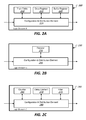
- FIGS. 2A , 2 B, and 2 C show different examples of different types of logic elements.
- FIG. 3A shows an example of a PLU programmed to perform a logic operation.
- FIG. 3B shows an example of a truth table.
- FIG. 4 shows another example of a PLU programmed to perform logical functions.
- FIG. 5 shows an example of a PLU programmed to perform encoding and decoding for a universal synchronous/asynchronous receiver/transmitter (USART).
- USART universal synchronous/asynchronous receiver/transmitter
- FIG. 6 shows an example of a PLU programmed for transferring and encoding data.
- FIG. 7 shows an example of a PLU programmed to be a shift register for a serial communication protocol.
- FIG. 8 shows an example of a PLU programmed for data buffer transmission.
- FIG. 9A shows an example of a PLU programmed to be an edge detector.
- FIG. 9B shows example signal graphs associated with the PLU of FIG. 9A .
- FIG. 10A shows an example of a PLU programmed to be an event counter.
- FIG. 10B shows example signal graphs associated with the PLU of FIG. 10A .
- FIG. 11 shows another example of a PLU architecture.
- FIG. 12 shows an example of a logic element architecture.
- FIG. 13 shows an example of a system on a chip architecture that includes a PLU.
- FIG. 14 shows another example of a logic element architecture.
- Systems can perform various types of activities. For a system that requires serial communication, there is a need to have a specific type of encoding for transmitting a frame.
- a possible approach is to implement in non-reconfigurable hardware a specific coding style such as Manchester encoding. In this case, such hardware cannot be altered to support a different type of coding style such as non-return-to-zero (NRZ). Thus, such hardware doesn't provide flexibility and may have a high cost of material due to the hardware's customization.
- Another possible approach is to implement the coding style in a software program running on a processor unit. The drawback is power consumption, since the processor unit has to be in an active mode to perform the coding style.
- the analog-digital-convertor (ADC) scan mode is such an example.
- the processor unit must be running when a full scan is completed (e.g., after eight conversions).
- a counter which generates an interrupt when the scan is completed.
- Some devices can (1) use a specific counter for this specific need, (2) use an existing system timer, or (3) leave the processor unit in the active state.
- the drawbacks here may include (1) using non-reconfigurable hardware that doesn't provide flexibly, (2) using only a portion of an existing resource (e.g., using an 8-bit count when a 3-bit counter is sufficient, (3) wasting power while the processor unit is in the active state, which has great consequences for systems running on battery power, or a combination thereof.
- a PLU is used to off-load a task, or a portion thereof, from the processor unit.
- a PLU can be programmed to detect the “CTRL+ALT+DEL” key sequence and send a wake-up interrupt to cause a processor unit to return to an active state.
- a PLU in general, can be programmed to perform a variety of functions. These functions can be performed by logic elements that are included in the PLU.
- a PLU includes logic elements of different types.
- a PLU can include logic elements of a first type that are each individually programmable to be one of a first set of functions and logic elements of a second type that are each individually programmable to be one of a second set of functions; the first and second sets of functions can be mutually exclusive or can have one or more functions in common.
- a programmable interconnect array (PIA), included in a PLU can be programmed to distribute one or more input signals to selected ones of the logic elements, distribute intermediate signals among the logic elements, and collect an output signal from a logic element and provide it as an output of the PLU.
- PPA programmable interconnect array
- Systems and devices can include one or more PLUs.
- PLUs can be programmed for a wide range of applications.
- applications suited for a PLU include controlling data transmission via a serial bit-stream, inverting data such as inverting data from a receive pin (R ⁇ D) or data to a transmit pin (T ⁇ D) pin on a universal synchronous/asynchronous receiver/transmitter (USART) bus, performing Manchester encoding/decoding using the USART, inserting dead time between power width modulation (PWM) pulses, or triggering an action only when a pre-determined number of events have been received or when a pre-determined number of pin levels are present at the same time.
- One or more described PLU can be implemented as high speed logic (e.g., logic circuitry operating at 60 or 70 MHz which has been fabricated under a 0.35 ⁇ m process).
- FIG. 1 shows an example of a programmable logic unit architecture.
- a PLU 100 includes a first logic element A 110 , a second logic element A 115 , a first logic element B 120 , a second logic element B 125 , a first logic element C 130 , and a second logic element C 135 . These logic elements are interconnected via a PIA 105 .
- the PIA 105 further is connectable to a clock selector 140 , clock sources 145 , internal peripheral bus 150 , a direct memory access (DMA) bus 160 , event system bus 165 , processor unit interface 170 , and external pin(s) 175 .
- DMA direct memory access
- the PIA 105 Based on a programming operation, the PIA 105 selectively forms one or more interconnections within a group including the one or more input interfaces, the one or more output interfaces, and the logic elements 110 , 115 , 120 , 125 , 130 , 135 .
- the PIA 105 includes the clock selector 140 .
- the one or more input interfaces can receive input signals from the clock selector 140 , clock sources 145 , internal peripheral bus 150 , a DMA bus 160 , event system bus 165 , processor unit interface 170 , external pin(s) 175 , or a combination thereof.
- the one or more output interfaces can provide an output signal(s) to one or more destinations such as an internal peripheral bus 150 , a DMA bus 160 , event system bus 165 , processor unit interface 170 , or external pin(s) 175 .
- the PIA 105 includes a network of multiplexers and demultiplexers. In some implementations, the PIA 105 includes a programmable switching fabric.
- the first logic element A 110 and the second logic element A 115 can be configured via a programming operation as a truth table, data register, or a buffer register. In some implementations, the first logic element A 110 and the second logic element A 115 include an 8-bit register. Other register bit sizes are possible, such as 16-bit or 32-bit.
- the first logic element B 120 and the second logic element B 125 can include a 4-bit decoder. Other decoder bit sizes are possible, such as 8-bit, 16-bit, or 32-bit.
- the first logic element C 130 and the second logic element C 135 can be configured via a programming operation as a counter, delay element, or a filter. In some implementations, the first logic element C 130 and the second logic element C 135 include a 4-bit register. Other register bit sizes are possible, such as 8-bit, 16-bit, or 32-bit.
- the internal peripheral bus 150 can connect the PLU 100 with one or more peripherals, e.g., a module that has a specific function.
- peripherals include a timer, universal synchronous/asynchronous receiver/transmitter (USART), and a serial peripheral interface (SPI).
- the PLU 100 is considered to be a peripheral.
- the event system bus 165 allows direct inter-peripheral communication and signaling.
- the event system bus 165 receives events from a peripheral and routes them to another peripheral.
- the DMA bus 160 can be used to transfer data between a memory (not shown) and the PLU 100 without directly involving a processor unit.
- DMA bus 160 is used to transfer data from one peripheral to another peripheral.
- the clock selector 140 can cause a selection of two or more clock sources 145 for one or more sequential logic operations performed by the PLU 100 .
- Programming the PLU 100 can include sending programming commands from a processor unit to the PLU 100 via the processor unit interface 170 .
- the PLU 100 stores programming settings in a memory such as a non-volatile memory or a volatile memory.
- a processor unit can dynamically reprogram the PLU 100 without requiring a power-cycle.
- components such as the PLU 100 and a processor unit compose a System-on-a-Chip (SoC).
- SoC System-on-a-Chip
- the SoC can be formed as an integrated circuit that is included in an integrated circuit package.
- the integrated circuit package can include electrical contacts, such as external contact pads or external pins, for external electrical connectivity.
- FIG. 2A shows an example of a logic element of a first type.
- a logic element A 200 includes a truth table 210 , data register 215 , buffer register 220 , and configuration & distribution logic 225 .
- the configuration & distribution element 225 can distribute an input signal to one of the truth table 210 , data register 215 , and buffer register 220 .
- the configuration & distribution element 225 can collect an output signal from one of the truth table 210 , data register 215 , and buffer register 220 .
- the configuration & distribution element 225 can provide the collected signal to a programmable interconnect array.
- the truth table 210 , the data register 215 , and the buffer register 220 are replaced by a single memory structure.
- a truth table 210 is used as a look-up table (LUT) for a decoder. Signal routing within the configuration & distribution element 225 can be controlled via a configuration input signal.
- LUT look-up table
- FIG. 2B shows an example of a logic element of a second type.
- a logic element B 230 includes a decoder 235 , and a configuration & distribution element 245 .
- the configuration & distribution element 225 can send signals to and receive signals from the decoder 235 .
- the decoder 235 can be programmed to be an encoder. In some cases, a decoder performs the same function as an encoder (e.g., for the same inputs, both the encoder and decoder produces the same output).
- FIG. 2C shows an example of a logic element of a third type.
- a logic element C 260 includes a counter 265 , delay element 270 , filter 275 , and configuration & distribution element 280 .
- the configuration & distribution element 225 can distribute an input signal to one of the counter 265 , delay element 270 , and filter 275 .
- the configuration & distribution element 225 can collect an output signal from one of the counter 265 , delay element 270 , and filter 275 .
- the configuration & distribution element 225 can provide the collected signal to a programmable interconnect array.
- FIG. 3A shows an example of a PLU programmed to perform a logic operation.
- a PLU 300 includes a logic element A 0 305 programmed to be a truth table and a logic element B 0 310 programmed to be a decoder. Based on three inputs to the logic element B 0 310 , the logic element B 0 310 looks up the corresponding output value via the logic element A 0 305 .
- a PIA (not shown) included in the PLU 300 is programmed to provide the logical connections depicted by FIG. 3A , where the solid arrows denote a programmed logical connection via the PIA. In this example, the PIA has been programmed to route three input signals from three input interfaces into logic element B 0 310 .
- An input interface can include an electrical connection with an electrical contact, e.g., one or more external pins or contact pads, to receive a signal. Further, the PIA has been programmed to route one or more intermediate signals between logic element A 0 305 and logic element B 0 310 . Further, the PIA has been programmed to route an output signal from logic element B 0 310 to an output interface of the PLU 300 .
- An output interface can include an electrical connection with an electrical contact, e.g., one or more external pins or contact pads, to provide a signal.
- FIG. 3B shows an example of a truth table.
- a truth table 350 includes an output for each 3-bit input value.
- the 3-bit input value can include a first bit from input 0 of FIG. 3A , a second bit from input 1 , and a third bit from input 2 .
- the truth table 350 can be stored in a data structure include in the logic element A 0 305 .
- For 3-bit input values there are a total of 8 different combinations of input values.
- the truth table 350 stores an output value for each possible input value.
- a logic element B 0 310 can send an input value to logic element A 0 305 .
- Logic element A 0 305 accesses the truth table 350 based on its received input, and sends a corresponding output value to logic element B 0 310 .
- FIG. 4 shows another example of a PLU programmed to perform logical functions.
- a PLU 400 is programmed to perform logical functions as depicted by the circuit schematic 450 in the lower portion of FIG. 4 .
- the PLU 400 includes a logic element A 0 405 programmed to be a first truth table that implements XOR logic, logic element B 0 420 programmed to be a decoder that uses the first truth table to perform a logic operation on its inputs (input 1 and input 2 ), logic element A 1 410 programmed to be a second truth table that implements XOR and AND logic, and logic element B 1 430 programmed to be a decoder that uses the second truth table to perform a logic operation on its inputs (input 3 , input 4 , and output from element B 0 420 ).
- the output of the PLU 400 is equivalent to the output of the circuit schematic 450 .
- a PIA (not shown) included in the PLU 400 is programmed to provide the logical connections depicted by FIG. 4 , where the solid arrows denote a programmed logical connection via the PIA.
- FIG. 5 shows an example of a PLU programmed to perform encoding and decoding for a USART.
- a PLU 500 can be programmed to be a Manchester encoder/decoder for a USART. Note that Manchester encoding is the same as Manchester decoding. Thus, given an input signal that is Manchester encoded, the PLU 500 produces a decoded output signal. Given an input signal that is not Manchester encoded, the PLU 500 produces a Manchester encoded output signal. Other types of encoding and decoding are possible such as non-return-to-zero (NRZ).
- NRFZ non-return-to-zero
- the PLU 500 includes a logic element A 0 510 programmed to be a truth table, a logic element A 1 515 programmed to be a truth table, logic element B 0 520 programmed to be a decoder, logic element B 1 525 programmed to be a decoder, logic element C 0 530 programmed to be a delay-by-one, and logic element C 1 535 programmed to be a delay-by-one.
- a delay-by-one is used to output a received input one clock cycle later.
- a PIA (not shown) included in the PLU 500 is programmed to provide the logical connections depicted by FIG. 5 , where the solid arrows denote a programmed logical connection via the PIA.
- the truth table stored in element A 0 510 is programmed to cause logic element B 0 520 to perform a XOR logic function on its inputs (e.g., R ⁇ D from external pin and an output from the clock source selector 505 ).
- the truth table stored in element A 1 515 is programmed to cause logic element B 1 525 to perform a XOR logic function on its inputs (e.g., T ⁇ D from USART peripheral and an output from the clock source selector 505 ).
- Manchester encoding and decoding operations are symmetric (encoding is an XOR of a clock signal and a data signal, and decoding is an XOR of an encoded data signal and a clock signal).
- a clock source selector 505 of the PLU 500 can select a clock input from two or more sources (e.g., internal source C 1 or external source C 2 ) based on whether the PLU 500 is operating as a master or a slave. Operating as a master, the clock source selector 505 selects a clock source from an internal source C 1 such as from an internal USART peripheral. Operating as a slave, the clock source selector 505 selects a clock source from an external source C 2 such as an external pin.
- sources e.g., internal source C 1 or external source C 2
- FIG. 6 shows an example of a PLU programmed for transferring and encoding data.
- a PLU 600 programmed for transferring and encoding data includes logic element A 0 610 programmed to be a data register, logic element A 1 620 programmed to be a truth table, logic element B 0 630 programmed to be an encoder, logic element B 1 640 programmed to be a decoder, and logic element C 0 650 programmed to be a counter.
- a DMA operation can load a data register of logic element A 0 610 with one or more values.
- the logic element B 1 640 produces an output for the PLU 500 .
- a clock signal can be applied to logic element C 0 650 and logic element B 1 640 .
- a first section of the PLU 600 (including logic element A 0 610 , logic element B 0 630 , and logic element C 0 650 ) is used to serialize data stored in the data register of logic element A 0 610 .
- Logic element B 0 630 outputs a serial data stream to a second section of the PLU 600 (including logic element A 1 620 and logic element B 1 640 ) which is used to encode the serial data stream for transmission via an external pin or on-chip peripheral.
- a PIA (not shown) included in the PLU 600 is programmed to provide the logical connections depicted by FIG. 6 , where the solid arrows denote a programmed logical connection via the PIA.
- FIG. 7 shows an example of a PLU programmed to be a shift register for a serial communication protocol.
- a PLU 700 programmed to be a shift register for a serial communication protocol includes logic element A 0 710 programmed to be a data register, logic element A 1 720 programmed to be a data register, logic element B 0 740 programmed to be a decoder, logic element C 0 730 programmed to be a counter, and logic element C 1 750 programmed to be a register.
- a PIA (not shown) included in the PLU 700 is programmed to provide the logical connections depicted by FIG. 7 , where the solid arrows denote a programmed logical connection via the PIA.
- Element A 0 710 and element A 1 720 can be used to store data to be transmitted or data that was received (START/STOP bit included).
- the PLU 700 can support both most significant bit (MSB) and least significant bit (LSB) first formats.
- MSB most significant bit
- Element C 1 750 is set as a register to hold a TOP value for the counter of element C 0 730 , where the TOP value is 10 since 10 bits are to be transmitted.
- the clock for the counter and decoder can be selectable via a clock selector that draws its inputs from an external pin (clock sent by a master) or internal peripheral (e.g., timer or event system). In this example, it is required that the clock period is a time bit period.
- the counter of element C 0 720 is incremented by 1.
- the counter is used as a bit index into an array composed out of the bit elements of the data registers of both element A 0 710 and element A 1 720 , and the corresponding bit is sent over the line. When the counter reaches the TOP, it is stopped (but not cleared, to maintain the STOP bit value).
- the PLU 700 can be programmed to transmit 8-bit USART data with the MSB first.
- Supposing data to be transmitted is 0x53 (hex), which is 01010011 in binary code
- the USART frame with MSB first looks like 0-01010011-1.
- Element A 0 710 and element A 1 720 are used to store the USART frame (xxxxxx00 10100111, where ‘x’ indicates a not-used bit-element of the register).
- Element C 0 730 is set as a decrement counter and initialized to 10. At each clock cycle, the counter of logic element C 0 730 is decremented by 1. As it is used as bit index for elements A 0 /A 1 , the corresponding bit is sent over the line. When the counter reaches the 0 value, the counter is stopped.
- FIG. 8 shows an example of a PLU programmed for data buffer transmission.
- a PLU 800 programmed for data buffer transmission includes logic element A 0 805 programmed to be a buffer register, logic element A 1 810 programmed to be a data register, logic element B 1 825 programmed to be a decoder, logic element C 0 840 programmed to be a byte counter, and logic element C 1 845 programmed to be a bit counter.
- a PIA (not shown) included in the PLU 800 is programmed to provide the logical connections depicted by FIG. 8 , where the solid arrows denote a programmed logical connection via the PIA.
- Logic element C 0 840 is used in this example to define the number of bytes to be sent (full or partial bytes).
- An output of logic element C 0 840 causes logic element B 1 825 to output signals to trigger DMA transfers between a memory location and buffer register.
- logic element A 0 805 acting as a buffer register, is used to store a byte received from the DMA. Based on the buffer register receiving the byte, the received byte is transferred to the data register of logic element A 1 810 .
- logic element A 1 810 uses an output of the decoder of logic element B 1 825 , logic element A 1 810 provides a serial bit stream to an external pin.
- the PLU 800 is included in a SoC, and the logic element A 1 810 provides a serial bit stream to an on-chip peripheral of the SoC.
- logic element C 1 845 being programmed to be a bit-counter, the bit-counter's TOP value is 8 while the byte-counter of logic element C 0 840 has not reached its TOP value, else, the bit-counter's TOP value is the number of bits to be transmitted during the last transfer.
- the byte-counter of logic element C 0 840 is set to 2, where a 0 value means no more DMA transfers or no transmissions.
- the PLU 800 has to do one complete byte transfer (8 bits) and one partial byte transfer (2 bits).
- a TOP value for the bit-counter of logic element C 1 845 is set to 8 for the first phase and then to 2 for the second phase. During the first phase, the bit-counter increments 8 times. During the second phase, the bit-counter resets to 0 and increments 2 times.
- FIG. 9A shows an example of a PLU programmed to be an edge detector.
- a PLU 900 programmed to be an edge detector includes logic element A 0 910 programmed to be a truth table, logic element B 0 920 programmed to be a decoder, and logic element C 0 930 programmed to be a delay.
- a PIA (not shown) included in the PLU 900 is programmed to provide the logical connections depicted by FIG. 9A , where the solid arrows denote a programmed logical connection via the PIA.
- To detect an edge on an input signal the signal is sampled one time (delayed) and gate logics are used to generate an output pulse.
- the logic element B 0 920 receives the input signal and a delayed version of the input signal via logic element C 0 930 . Using the truth table and its inputs, logic element B 0 920 produces an output.
- the truth table can be programmed to cause a pulse on a falling edge, a pulse on a rising edge, or both.
- using clock options and timers allows the PLU 900 to generate pulses, which can be used for communication-based applications.
- using clock options and timers allows the PLU 900 to insert dead time periods on PWM signals, which can be useful for motor control applications.
- FIG. 9B shows example signal graphs associated with the PLU of FIG. 9A .
- the graphs 950 show an input signal, a delayed input signal that is produced by element C 0 930 , and an output signal that is produced by logic element B 0 920 .
- the output includes a pulse on a falling edge and a subsequent pulse on the rising edge.
- FIG. 10A shows an example of a PLU programmed to be an event counter.
- a PLU 1000 programmed to be an event counter includes logic element A 0 1010 programmed to be a truth table, logic element B 0 1020 programmed to be a decoder, and logic element C 0 1030 programmed to be a counter (which receives inputs from an event system).
- a PIA (not shown) included in the PLU 1000 is programmed to provide the logical connections depicted by FIG. 10A , where the solid arrows denote a programmed logical connection via the PIA.
- Logic element B 0 1020 receives inputs from an event system (e.g., EV 1 and EV 2 ) and an output of the logic element A 0 1010 .
- an event system e.g., EV 1 and EV 2
- logic element A 0 1010 causes logic element B 0 1020 to be OR logic.
- either a pulse on EV 1 or EV 2 causes logic element B 0 1020 to output a pulse to the counter of logic element C 0 .
- Logic element C 0 1030 receives an input from logic element B 0 1020 and provides an output to the event system. For example, when the counter reaches a pre-determined TOP value, logic element B 0 1020 asserts a pulse to the event system.
- FIG. 10B shows example signal graphs associated with the PLU of FIG. 10A .
- the system does not need to wake-up on each event.
- a typical example is the ADC scan mode, where an ADC performs conversions using one or more channels.
- the DMA can be used to transfer converted data to one or more memory locations, but the system is required to be informed when the ADC scan is completed. In this example, the system is required to be informed when 4 events are received.
- the PLU 1000 can signalize the scan completion to the event system.
- the graphs 1050 show a first input signal (EV 1 ) from the event system, a second input signal (EV 2 ) from the event system, and an output to the event system that is produced by the logic element C 0 1030 . After the fourth event, logic element C 0 1030 asserts a signal on the event system and then resets the counter back to zero.
- FIG. 11 shows another example of a PLU architecture.
- a PLU 1100 can include a PIA that is split into an input distributor 1120 and an output distributor 1130 .
- the input distributor 1120 can route signals from outside the PLU 1100 (e.g., one more clock signals, peripheral input, external pin input, event system, or DMA) to logic elements 1140 a , 1140 b , and 1140 c inside of the PLU 1100 .
- One or more clock signals can be provided to one or more logic elements 1140 a - c for a sequential logic operation(s).
- the output(s) of one or more logic elements 1140 a - c can be turned into one or more inputs.
- the input distributor 1120 can route a logic element output(s) to a logic element input(s).
- the output distributor 1130 can route signals from one or more of the logic elements 1140 a - c to one or more destinations such as a peripheral, external pin, event system, DMA, or interrupt.
- FIG. 12 shows an example of a logic element architecture.
- a controller can configure a logic element 1200 to be one of three different types functions (F 1 , F 2 , or F 3 ) via a programmable selector 1245 included in the logic element 1200 .
- the logic element 1200 provides an input 1205 to multiple logic circuits such as logic circuit F 1 1210 , logic circuit F 2 1220 , and logic circuit F 3 1230 that implement respectively the different types of functions supported by the logic element 1200 .
- the outputs of the logic circuits 1210 , 1220 , 1230 are provided to a multiplexer 1240 . Based on an output of the programmable selector 1245 , the multiplexer 1240 selects one of its inputs and provides the selected input as an output 1250 for the logic element 1200 .
- FIG. 13 shows an example of a system on a chip architecture that includes a PLU.
- a system on a chip (SoC) 1300 can include a bus matrix 1305 , processor unit 1310 , RAM 1315 , non-volatile (NV) memory 1320 , DMA controller 1325 , and peripheral bridge 1330 .
- the bus matrix 1305 routes signals among its connected components such as the processor unit 1310 , RAM 1315 , NV memory 1320 , DMA controller 1325 , and peripheral bridge 1330 .
- the processor unit 1310 can include one or more processors.
- the peripheral bridge 1330 is connected with a timer 1335 , a PLU 1340 , peripheral-A 1350 , and peripheral-B 1360 .
- the DMA controller 1325 controls memory operations between peripheral components (e.g., PLU 1340 , peripheral-A 1350 , and peripheral-B 1360 ) and memory components such as the RAM 1315 , off-chip memory (if available), or both.
- the processor unit 1310 is configured to program the PLU 1340 to receive at least one of the one or more input signals from a peripheral 1350 , 1360 .
- the processor unit 1310 is configured to program the PLU 1340 to provide its output signal to a peripheral 1350 , 1360 .
- the processor unit 1310 programs the PLU 1340 by sending commands via the peripheral bridge 1330 to the PLU 1340 .
- commands include a command to program a logic element of the PLU 1340 to perform a function, a command to program a PIA of the PLU 1340 on how to interconnect logic elements, a command to set a register included in the PLU 1340 , a command to set an input pathway(s), and a command to set an output pathway(s).
- Other types of commands are possible.
- the SoC 1300 can be formed as an integrated circuit that is included in an integrated circuit package.
- the integrated circuit package can include electrical contacts (such as external contact pads or external pins) for external electrical connectivity.
- a portion of the electrical contacts are general purpose input output (GPIO) pins.
- Some of the peripheral components such as PLU 1340 , peripheral-A 1350 , and peripheral-B 1360 can be connected with external pins of the SoC 1300 such that a peripheral component can send signals to an external destination or receive signals from an external source.
- at least some of the peripheral components have dedicated external pins called GPIO pins 1345 , 1355 , 1365 .
- GPIO pins can be configured to be input pins, output pins, or both.
- the SoC 1300 includes multiple PLUs, which can each be individually programmed.
- FIG. 14 shows another example of a logic element architecture.
- a logic element 1400 includes circuitry for a counter, a delay element, and a filter.
- the counter can be associated with a TOP value, which can be pre-programmed during a programming cycle.
- the counter counts from 0 up to the TOP value, the output of the logic element 1400 is the value of the counter.
- the counter In a first programmable mode, the counter can be programmed to never start, and always outputs a zero.
- the counter In a second programmable mode, the counter can re-start. For example, based on reaching the TOP value, the counter will reset to a pre-determined value such as zero.
- the counter stops at the TOP value and continues to output the TOP value.
- the delay element of the logic element 1400 can include one or more flip-flops (e.g., FF 1 , FF 2 , FF 3 , and FF 4 ).
- the output of the logic element 1400 programmed as a delay element is based on the n-th flip-flop, where n is the TOP value associated with the counter.
- n is the TOP value associated with the counter.
- the output of FF 1 can be used as the output of the logic element 1400 if a one cycle delay is required, whereas the output of FF 4 can be used if a four cycle delay is required.
- the counter value is set to the TOP value and set to not increment or decrement this value; where a MUX controller selects a flip-flop output based on the counter value.
- the filter of the logic element 1400 can include a signal that is based on a predetermined voltage source such as VSS which is zero.
- VSS a predetermined voltage source
- the output of the logic element 1400 programmed as a filter is based on VSS while the counter has not reached the TOP value.
- the MUX command can select the n-th flip-flop as the output of the logic element 1400 .
Abstract
Description
Claims (27)
Priority Applications (4)
| Application Number | Priority Date | Filing Date | Title |
|---|---|---|---|
| US13/304,287 US8415975B1 (en) | 2011-11-23 | 2011-11-23 | Programmable logic unit |
| DE202012103054U DE202012103054U1 (en) | 2011-11-23 | 2012-08-13 | Programmable logic unit |
| US13/858,757 US9083339B2 (en) | 2011-11-23 | 2013-04-08 | Programmable logic unit |
| US14/795,806 US10049071B2 (en) | 2011-11-23 | 2015-07-09 | Programmable logic unit |
Applications Claiming Priority (1)
| Application Number | Priority Date | Filing Date | Title |
|---|---|---|---|
| US13/304,287 US8415975B1 (en) | 2011-11-23 | 2011-11-23 | Programmable logic unit |
Related Child Applications (1)
| Application Number | Title | Priority Date | Filing Date |
|---|---|---|---|
| US13/858,757 Continuation US9083339B2 (en) | 2011-11-23 | 2013-04-08 | Programmable logic unit |
Publications (1)
| Publication Number | Publication Date |
|---|---|
| US8415975B1 true US8415975B1 (en) | 2013-04-09 |
Family
ID=46967815
Family Applications (3)
| Application Number | Title | Priority Date | Filing Date |
|---|---|---|---|
| US13/304,287 Active US8415975B1 (en) | 2011-11-23 | 2011-11-23 | Programmable logic unit |
| US13/858,757 Active 2032-05-12 US9083339B2 (en) | 2011-11-23 | 2013-04-08 | Programmable logic unit |
| US14/795,806 Active 2033-02-16 US10049071B2 (en) | 2011-11-23 | 2015-07-09 | Programmable logic unit |
Family Applications After (2)
| Application Number | Title | Priority Date | Filing Date |
|---|---|---|---|
| US13/858,757 Active 2032-05-12 US9083339B2 (en) | 2011-11-23 | 2013-04-08 | Programmable logic unit |
| US14/795,806 Active 2033-02-16 US10049071B2 (en) | 2011-11-23 | 2015-07-09 | Programmable logic unit |
Country Status (2)
| Country | Link |
|---|---|
| US (3) | US8415975B1 (en) |
| DE (1) | DE202012103054U1 (en) |
Cited By (3)
| Publication number | Priority date | Publication date | Assignee | Title |
|---|---|---|---|---|
| US20150146832A1 (en) * | 2013-11-27 | 2015-05-28 | Microchip Technology Incorporated | Main Clock High Precision Oscillator |
| US9859896B1 (en) * | 2015-09-11 | 2018-01-02 | Xilinx, Inc. | Distributed multi-die routing in a multi-chip module |
| US10049071B2 (en) | 2011-11-23 | 2018-08-14 | Atmel Corporation | Programmable logic unit |
Families Citing this family (1)
| Publication number | Priority date | Publication date | Assignee | Title |
|---|---|---|---|---|
| US10361048B2 (en) * | 2016-05-11 | 2019-07-23 | Eaton Intelligent Power Limited | Pyrotechnic circuit protection systems, modules, and methods |
Citations (7)
| Publication number | Priority date | Publication date | Assignee | Title |
|---|---|---|---|---|
| US6275065B1 (en) * | 1996-04-09 | 2001-08-14 | Altera Corporation | Programmable logic integrated circuit architecture incorporating a lonely register |
| US6340897B1 (en) * | 1995-03-22 | 2002-01-22 | Altera Corporation | Programmable logic array integrated circuit with general-purpose memory configurable as a random access or FIFO memory |
| US6362646B1 (en) * | 1997-06-20 | 2002-03-26 | Altera Corporation | Method and apparatus for reducing memory resources in a programmable logic device |
| US6810513B1 (en) * | 2002-06-19 | 2004-10-26 | Altera Corporation | Method and apparatus of programmable interconnect array with configurable multiplexer |
| US6898101B1 (en) * | 1997-12-16 | 2005-05-24 | Cypress Semiconductor Corp. | Microcontroller with programmable logic on a single chip |
| US7058880B1 (en) * | 2001-12-26 | 2006-06-06 | Altera Corporation | Techniques for programming and verifying data in a programmable circuit |
| US7161384B1 (en) * | 2002-11-21 | 2007-01-09 | Altera Corporation | Flexible macrocell interconnect |
Family Cites Families (8)
| Publication number | Priority date | Publication date | Assignee | Title |
|---|---|---|---|---|
| JP3993717B2 (en) * | 1998-09-24 | 2007-10-17 | 富士通株式会社 | Semiconductor integrated circuit device |
| US6774672B1 (en) * | 2002-12-30 | 2004-08-10 | Actel Corporation | Field-programmable gate array architecture |
| US7575561B2 (en) * | 2004-01-26 | 2009-08-18 | Knit Rite, Inc. | Above knee shrinker |
| US7818705B1 (en) * | 2005-04-08 | 2010-10-19 | Altera Corporation | Method and apparatus for implementing a field programmable gate array architecture with programmable clock skew |
| US7576561B1 (en) * | 2007-11-13 | 2009-08-18 | Xilinx, Inc. | Device and method of configuring a device having programmable logic |
| US8488623B2 (en) * | 2010-07-28 | 2013-07-16 | Altera Corporation | Scalable interconnect modules with flexible channel bonding |
| US8415975B1 (en) | 2011-11-23 | 2013-04-09 | Atmel Corporation | Programmable logic unit |
| US8773164B1 (en) * | 2012-11-01 | 2014-07-08 | Xilinx, Inc. | Programmable interconnect network |
-
2011
- 2011-11-23 US US13/304,287 patent/US8415975B1/en active Active
-
2012
- 2012-08-13 DE DE202012103054U patent/DE202012103054U1/en not_active Expired - Lifetime
-
2013
- 2013-04-08 US US13/858,757 patent/US9083339B2/en active Active
-
2015
- 2015-07-09 US US14/795,806 patent/US10049071B2/en active Active
Patent Citations (8)
| Publication number | Priority date | Publication date | Assignee | Title |
|---|---|---|---|---|
| US6340897B1 (en) * | 1995-03-22 | 2002-01-22 | Altera Corporation | Programmable logic array integrated circuit with general-purpose memory configurable as a random access or FIFO memory |
| US6275065B1 (en) * | 1996-04-09 | 2001-08-14 | Altera Corporation | Programmable logic integrated circuit architecture incorporating a lonely register |
| US6362646B1 (en) * | 1997-06-20 | 2002-03-26 | Altera Corporation | Method and apparatus for reducing memory resources in a programmable logic device |
| US6898101B1 (en) * | 1997-12-16 | 2005-05-24 | Cypress Semiconductor Corp. | Microcontroller with programmable logic on a single chip |
| US7480165B1 (en) * | 1997-12-16 | 2009-01-20 | Mann Eric N | Microcontroller with programmable logic |
| US7058880B1 (en) * | 2001-12-26 | 2006-06-06 | Altera Corporation | Techniques for programming and verifying data in a programmable circuit |
| US6810513B1 (en) * | 2002-06-19 | 2004-10-26 | Altera Corporation | Method and apparatus of programmable interconnect array with configurable multiplexer |
| US7161384B1 (en) * | 2002-11-21 | 2007-01-09 | Altera Corporation | Flexible macrocell interconnect |
Cited By (5)
| Publication number | Priority date | Publication date | Assignee | Title |
|---|---|---|---|---|
| US10049071B2 (en) | 2011-11-23 | 2018-08-14 | Atmel Corporation | Programmable logic unit |
| US20150146832A1 (en) * | 2013-11-27 | 2015-05-28 | Microchip Technology Incorporated | Main Clock High Precision Oscillator |
| US9509321B2 (en) * | 2013-11-27 | 2016-11-29 | Microchip Technology Incorporated | Main clock high precision oscillator |
| TWI628917B (en) * | 2013-11-27 | 2018-07-01 | 美商微晶片科技公司 | Main clock high precision oscillator |
| US9859896B1 (en) * | 2015-09-11 | 2018-01-02 | Xilinx, Inc. | Distributed multi-die routing in a multi-chip module |
Also Published As
| Publication number | Publication date |
|---|---|
| US9083339B2 (en) | 2015-07-14 |
| US20150309957A1 (en) | 2015-10-29 |
| US10049071B2 (en) | 2018-08-14 |
| US20130222012A1 (en) | 2013-08-29 |
| DE202012103054U1 (en) | 2012-09-03 |
Similar Documents
| Publication | Publication Date | Title |
|---|---|---|
| US10516397B2 (en) | System level interconnect with programmable switching | |
| US6507214B1 (en) | Digital configurable macro architecture | |
| US10049071B2 (en) | Programmable logic unit | |
| US7385417B1 (en) | Dual slice architectures for programmable logic devices | |
| US10560102B1 (en) | Field programmable gate array including coupled lookup tables | |
| US7638903B2 (en) | Power supply selection for multiple circuits on an integrated circuit | |
| EP2722989B1 (en) | Methods and apparatus for building bus interconnection networks using programmable interconnection resources | |
| US20140013022A1 (en) | Universal digital block interconnection and channel routing | |
| EP2700170B1 (en) | Configurable logic cells | |
| US8675681B2 (en) | Communication within an integrated circuit including an array of interconnected programmable logic elements | |
| US6255846B1 (en) | Programmable logic devices with enhanced multiplexing capabilities | |
| US20160182054A1 (en) | Configurable Logic Circuit Including Dynamic Lookup Table | |
| US6975154B1 (en) | Reduced power consumption clock network | |
| US7675321B1 (en) | Dual-slice architectures for programmable logic devices | |
| CN109947395B (en) | Programmable logic unit structure and chip | |
| US20120271968A1 (en) | Logic device for combining various interrupt sources into a single interrupt source and various signal sources to control drive strength | |
| US10949204B2 (en) | Microcontroller with configurable logic peripheral | |
| CN114026552B (en) | Microcontroller with configurable logic peripherals | |
| EP2700167B1 (en) | Configurable logic cells | |
| US7378872B1 (en) | Programmable logic device architecture with multiple slice types | |
| KR101922019B1 (en) | Selecting four signals from sixteen inputs | |
| GB2325071A (en) | Programmable logic array |
Legal Events
| Date | Code | Title | Description |
|---|---|---|---|
| AS | Assignment |
Owner name: ATMEL NANTES S.A.S., FRANCE Free format text: ASSIGNMENT OF ASSIGNORS INTEREST;ASSIGNOR:BIRSAN, LAURENTIU;REEL/FRAME:027517/0533 Effective date: 20111123 Owner name: ATMEL CORPORATION, CALIFORNIA Free format text: ASSIGNMENT OF ASSIGNORS INTEREST;ASSIGNOR:ATMEL NANTES S.A.S.;REEL/FRAME:027518/0203 Effective date: 20120106 Owner name: ATMEL CORPORATION, CALIFORNIA Free format text: ASSIGNMENT OF ASSIGNORS INTEREST;ASSIGNOR:DANIELSEN, STEIN;REEL/FRAME:027517/0578 Effective date: 20111123 |
|
| STCF | Information on status: patent grant |
Free format text: PATENTED CASE |
|
| AS | Assignment |
Owner name: MORGAN STANLEY SENIOR FUNDING, INC. AS ADMINISTRATIVE AGENT, NEW YORK Free format text: PATENT SECURITY AGREEMENT;ASSIGNOR:ATMEL CORPORATION;REEL/FRAME:031912/0173 Effective date: 20131206 Owner name: MORGAN STANLEY SENIOR FUNDING, INC. AS ADMINISTRAT Free format text: PATENT SECURITY AGREEMENT;ASSIGNOR:ATMEL CORPORATION;REEL/FRAME:031912/0173 Effective date: 20131206 |
|
| AS | Assignment |
Owner name: ATMEL CORPORATION, CALIFORNIA Free format text: TERMINATION AND RELEASE OF SECURITY INTEREST IN PATENT COLLATERAL;ASSIGNOR:MORGAN STANLEY SENIOR FUNDING, INC.;REEL/FRAME:038376/0001 Effective date: 20160404 |
|
| FPAY | Fee payment |
Year of fee payment: 4 |
|
| AS | Assignment |
Owner name: JPMORGAN CHASE BANK, N.A., AS ADMINISTRATIVE AGENT, ILLINOIS Free format text: SECURITY INTEREST;ASSIGNOR:ATMEL CORPORATION;REEL/FRAME:041715/0747 Effective date: 20170208 Owner name: JPMORGAN CHASE BANK, N.A., AS ADMINISTRATIVE AGENT Free format text: SECURITY INTEREST;ASSIGNOR:ATMEL CORPORATION;REEL/FRAME:041715/0747 Effective date: 20170208 |
|
| AS | Assignment |
Owner name: JPMORGAN CHASE BANK, N.A., AS ADMINISTRATIVE AGENT, ILLINOIS Free format text: SECURITY INTEREST;ASSIGNORS:MICROCHIP TECHNOLOGY INCORPORATED;SILICON STORAGE TECHNOLOGY, INC.;ATMEL CORPORATION;AND OTHERS;REEL/FRAME:046426/0001 Effective date: 20180529 Owner name: JPMORGAN CHASE BANK, N.A., AS ADMINISTRATIVE AGENT Free format text: SECURITY INTEREST;ASSIGNORS:MICROCHIP TECHNOLOGY INCORPORATED;SILICON STORAGE TECHNOLOGY, INC.;ATMEL CORPORATION;AND OTHERS;REEL/FRAME:046426/0001 Effective date: 20180529 |
|
| AS | Assignment |
Owner name: WELLS FARGO BANK, NATIONAL ASSOCIATION, AS NOTES COLLATERAL AGENT, CALIFORNIA Free format text: SECURITY INTEREST;ASSIGNORS:MICROCHIP TECHNOLOGY INCORPORATED;SILICON STORAGE TECHNOLOGY, INC.;ATMEL CORPORATION;AND OTHERS;REEL/FRAME:047103/0206 Effective date: 20180914 Owner name: WELLS FARGO BANK, NATIONAL ASSOCIATION, AS NOTES C Free format text: SECURITY INTEREST;ASSIGNORS:MICROCHIP TECHNOLOGY INCORPORATED;SILICON STORAGE TECHNOLOGY, INC.;ATMEL CORPORATION;AND OTHERS;REEL/FRAME:047103/0206 Effective date: 20180914 |
|
| AS | Assignment |
Owner name: JPMORGAN CHASE BANK, N.A., AS ADMINISTRATIVE AGENT, DELAWARE Free format text: SECURITY INTEREST;ASSIGNORS:MICROCHIP TECHNOLOGY INC.;SILICON STORAGE TECHNOLOGY, INC.;ATMEL CORPORATION;AND OTHERS;REEL/FRAME:053311/0305 Effective date: 20200327 |
|
| AS | Assignment |
Owner name: MICROCHIP TECHNOLOGY INC., ARIZONA Free format text: RELEASE BY SECURED PARTY;ASSIGNOR:JPMORGAN CHASE BANK, N.A, AS ADMINISTRATIVE AGENT;REEL/FRAME:053466/0011 Effective date: 20200529 Owner name: SILICON STORAGE TECHNOLOGY, INC., ARIZONA Free format text: RELEASE BY SECURED PARTY;ASSIGNOR:JPMORGAN CHASE BANK, N.A, AS ADMINISTRATIVE AGENT;REEL/FRAME:053466/0011 Effective date: 20200529 Owner name: ATMEL CORPORATION, ARIZONA Free format text: RELEASE BY SECURED PARTY;ASSIGNOR:JPMORGAN CHASE BANK, N.A, AS ADMINISTRATIVE AGENT;REEL/FRAME:053466/0011 Effective date: 20200529 Owner name: MICROSEMI STORAGE SOLUTIONS, INC., ARIZONA Free format text: RELEASE BY SECURED PARTY;ASSIGNOR:JPMORGAN CHASE BANK, N.A, AS ADMINISTRATIVE AGENT;REEL/FRAME:053466/0011 Effective date: 20200529 Owner name: MICROSEMI CORPORATION, CALIFORNIA Free format text: RELEASE BY SECURED PARTY;ASSIGNOR:JPMORGAN CHASE BANK, N.A, AS ADMINISTRATIVE AGENT;REEL/FRAME:053466/0011 Effective date: 20200529 |
|
| AS | Assignment |
Owner name: WELLS FARGO BANK, NATIONAL ASSOCIATION, MINNESOTA Free format text: SECURITY INTEREST;ASSIGNORS:MICROCHIP TECHNOLOGY INC.;SILICON STORAGE TECHNOLOGY, INC.;ATMEL CORPORATION;AND OTHERS;REEL/FRAME:053468/0705 Effective date: 20200529 |
|
| MAFP | Maintenance fee payment |
Free format text: PAYMENT OF MAINTENANCE FEE, 8TH YEAR, LARGE ENTITY (ORIGINAL EVENT CODE: M1552); ENTITY STATUS OF PATENT OWNER: LARGE ENTITY Year of fee payment: 8 |
|
| AS | Assignment |
Owner name: WELLS FARGO BANK, NATIONAL ASSOCIATION, AS COLLATERAL AGENT, MINNESOTA Free format text: SECURITY INTEREST;ASSIGNORS:MICROCHIP TECHNOLOGY INCORPORATED;SILICON STORAGE TECHNOLOGY, INC.;ATMEL CORPORATION;AND OTHERS;REEL/FRAME:055671/0612 Effective date: 20201217 |
|
| AS | Assignment |
Owner name: WELLS FARGO BANK, NATIONAL ASSOCIATION, AS NOTES COLLATERAL AGENT, MINNESOTA Free format text: SECURITY INTEREST;ASSIGNORS:MICROCHIP TECHNOLOGY INCORPORATED;SILICON STORAGE TECHNOLOGY, INC.;ATMEL CORPORATION;AND OTHERS;REEL/FRAME:057935/0474 Effective date: 20210528 |
|
| AS | Assignment |
Owner name: MICROSEMI STORAGE SOLUTIONS, INC., ARIZONA Free format text: RELEASE BY SECURED PARTY;ASSIGNOR:JPMORGAN CHASE BANK, N.A., AS ADMINISTRATIVE AGENT;REEL/FRAME:059333/0222 Effective date: 20220218 Owner name: MICROSEMI CORPORATION, ARIZONA Free format text: RELEASE BY SECURED PARTY;ASSIGNOR:JPMORGAN CHASE BANK, N.A., AS ADMINISTRATIVE AGENT;REEL/FRAME:059333/0222 Effective date: 20220218 Owner name: ATMEL CORPORATION, ARIZONA Free format text: RELEASE BY SECURED PARTY;ASSIGNOR:JPMORGAN CHASE BANK, N.A., AS ADMINISTRATIVE AGENT;REEL/FRAME:059333/0222 Effective date: 20220218 Owner name: SILICON STORAGE TECHNOLOGY, INC., ARIZONA Free format text: RELEASE BY SECURED PARTY;ASSIGNOR:JPMORGAN CHASE BANK, N.A., AS ADMINISTRATIVE AGENT;REEL/FRAME:059333/0222 Effective date: 20220218 Owner name: MICROCHIP TECHNOLOGY INCORPORATED, ARIZONA Free format text: RELEASE BY SECURED PARTY;ASSIGNOR:JPMORGAN CHASE BANK, N.A., AS ADMINISTRATIVE AGENT;REEL/FRAME:059333/0222 Effective date: 20220218 |
|
| AS | Assignment |
Owner name: ATMEL CORPORATION, ARIZONA Free format text: RELEASE BY SECURED PARTY;ASSIGNOR:JPMORGAN CHASE BANK, N.A., AS ADMINISTRATIVE AGENT;REEL/FRAME:059262/0105 Effective date: 20220218 |
|
| AS | Assignment |
Owner name: MICROSEMI STORAGE SOLUTIONS, INC., ARIZONA Free format text: RELEASE BY SECURED PARTY;ASSIGNOR:WELLS FARGO BANK, NATIONAL ASSOCIATION, AS NOTES COLLATERAL AGENT;REEL/FRAME:059358/0001 Effective date: 20220228 Owner name: MICROSEMI CORPORATION, ARIZONA Free format text: RELEASE BY SECURED PARTY;ASSIGNOR:WELLS FARGO BANK, NATIONAL ASSOCIATION, AS NOTES COLLATERAL AGENT;REEL/FRAME:059358/0001 Effective date: 20220228 Owner name: ATMEL CORPORATION, ARIZONA Free format text: RELEASE BY SECURED PARTY;ASSIGNOR:WELLS FARGO BANK, NATIONAL ASSOCIATION, AS NOTES COLLATERAL AGENT;REEL/FRAME:059358/0001 Effective date: 20220228 Owner name: SILICON STORAGE TECHNOLOGY, INC., ARIZONA Free format text: RELEASE BY SECURED PARTY;ASSIGNOR:WELLS FARGO BANK, NATIONAL ASSOCIATION, AS NOTES COLLATERAL AGENT;REEL/FRAME:059358/0001 Effective date: 20220228 Owner name: MICROCHIP TECHNOLOGY INCORPORATED, ARIZONA Free format text: RELEASE BY SECURED PARTY;ASSIGNOR:WELLS FARGO BANK, NATIONAL ASSOCIATION, AS NOTES COLLATERAL AGENT;REEL/FRAME:059358/0001 Effective date: 20220228 |
|
| AS | Assignment |
Owner name: MICROSEMI STORAGE SOLUTIONS, INC., ARIZONA Free format text: RELEASE BY SECURED PARTY;ASSIGNOR:WELLS FARGO BANK, NATIONAL ASSOCIATION, AS NOTES COLLATERAL AGENT;REEL/FRAME:059863/0400 Effective date: 20220228 Owner name: MICROSEMI CORPORATION, ARIZONA Free format text: RELEASE BY SECURED PARTY;ASSIGNOR:WELLS FARGO BANK, NATIONAL ASSOCIATION, AS NOTES COLLATERAL AGENT;REEL/FRAME:059863/0400 Effective date: 20220228 Owner name: ATMEL CORPORATION, ARIZONA Free format text: RELEASE BY SECURED PARTY;ASSIGNOR:WELLS FARGO BANK, NATIONAL ASSOCIATION, AS NOTES COLLATERAL AGENT;REEL/FRAME:059863/0400 Effective date: 20220228 Owner name: SILICON STORAGE TECHNOLOGY, INC., ARIZONA Free format text: RELEASE BY SECURED PARTY;ASSIGNOR:WELLS FARGO BANK, NATIONAL ASSOCIATION, AS NOTES COLLATERAL AGENT;REEL/FRAME:059863/0400 Effective date: 20220228 Owner name: MICROCHIP TECHNOLOGY INCORPORATED, ARIZONA Free format text: RELEASE BY SECURED PARTY;ASSIGNOR:WELLS FARGO BANK, NATIONAL ASSOCIATION, AS NOTES COLLATERAL AGENT;REEL/FRAME:059863/0400 Effective date: 20220228 |
|
| AS | Assignment |
Owner name: MICROSEMI STORAGE SOLUTIONS, INC., ARIZONA Free format text: RELEASE BY SECURED PARTY;ASSIGNOR:WELLS FARGO BANK, NATIONAL ASSOCIATION, AS NOTES COLLATERAL AGENT;REEL/FRAME:059363/0001 Effective date: 20220228 Owner name: MICROSEMI CORPORATION, ARIZONA Free format text: RELEASE BY SECURED PARTY;ASSIGNOR:WELLS FARGO BANK, NATIONAL ASSOCIATION, AS NOTES COLLATERAL AGENT;REEL/FRAME:059363/0001 Effective date: 20220228 Owner name: ATMEL CORPORATION, ARIZONA Free format text: RELEASE BY SECURED PARTY;ASSIGNOR:WELLS FARGO BANK, NATIONAL ASSOCIATION, AS NOTES COLLATERAL AGENT;REEL/FRAME:059363/0001 Effective date: 20220228 Owner name: SILICON STORAGE TECHNOLOGY, INC., ARIZONA Free format text: RELEASE BY SECURED PARTY;ASSIGNOR:WELLS FARGO BANK, NATIONAL ASSOCIATION, AS NOTES COLLATERAL AGENT;REEL/FRAME:059363/0001 Effective date: 20220228 Owner name: MICROCHIP TECHNOLOGY INCORPORATED, ARIZONA Free format text: RELEASE BY SECURED PARTY;ASSIGNOR:WELLS FARGO BANK, NATIONAL ASSOCIATION, AS NOTES COLLATERAL AGENT;REEL/FRAME:059363/0001 Effective date: 20220228 |
|
| AS | Assignment |
Owner name: MICROSEMI STORAGE SOLUTIONS, INC., ARIZONA Free format text: RELEASE BY SECURED PARTY;ASSIGNOR:WELLS FARGO BANK, NATIONAL ASSOCIATION, AS NOTES COLLATERAL AGENT;REEL/FRAME:060894/0437 Effective date: 20220228 Owner name: MICROSEMI CORPORATION, ARIZONA Free format text: RELEASE BY SECURED PARTY;ASSIGNOR:WELLS FARGO BANK, NATIONAL ASSOCIATION, AS NOTES COLLATERAL AGENT;REEL/FRAME:060894/0437 Effective date: 20220228 Owner name: ATMEL CORPORATION, ARIZONA Free format text: RELEASE BY SECURED PARTY;ASSIGNOR:WELLS FARGO BANK, NATIONAL ASSOCIATION, AS NOTES COLLATERAL AGENT;REEL/FRAME:060894/0437 Effective date: 20220228 Owner name: SILICON STORAGE TECHNOLOGY, INC., ARIZONA Free format text: RELEASE BY SECURED PARTY;ASSIGNOR:WELLS FARGO BANK, NATIONAL ASSOCIATION, AS NOTES COLLATERAL AGENT;REEL/FRAME:060894/0437 Effective date: 20220228 Owner name: MICROCHIP TECHNOLOGY INCORPORATED, ARIZONA Free format text: RELEASE BY SECURED PARTY;ASSIGNOR:WELLS FARGO BANK, NATIONAL ASSOCIATION, AS NOTES COLLATERAL AGENT;REEL/FRAME:060894/0437 Effective date: 20220228 |