US8331211B2 - Optical pickup device - Google Patents
Optical pickup device Download PDFInfo
- Publication number
- US8331211B2 US8331211B2 US13/186,833 US201113186833A US8331211B2 US 8331211 B2 US8331211 B2 US 8331211B2 US 201113186833 A US201113186833 A US 201113186833A US 8331211 B2 US8331211 B2 US 8331211B2
- Authority
- US
- United States
- Prior art keywords
- light
- area
- sensors
- reflected light
- areas
- Prior art date
- Legal status (The legal status is an assumption and is not a legal conclusion. Google has not performed a legal analysis and makes no representation as to the accuracy of the status listed.)
- Expired - Fee Related
Links
Images


Classifications
-
- G—PHYSICS
- G11—INFORMATION STORAGE
- G11B—INFORMATION STORAGE BASED ON RELATIVE MOVEMENT BETWEEN RECORD CARRIER AND TRANSDUCER
- G11B7/00—Recording or reproducing by optical means, e.g. recording using a thermal beam of optical radiation by modifying optical properties or the physical structure, reproducing using an optical beam at lower power by sensing optical properties; Record carriers therefor
- G11B7/12—Heads, e.g. forming of the optical beam spot or modulation of the optical beam
- G11B7/135—Means for guiding the beam from the source to the record carrier or from the record carrier to the detector
- G11B7/1372—Lenses
- G11B7/1378—Separate aberration correction lenses; Cylindrical lenses to generate astigmatism; Beam expanders
-
- G—PHYSICS
- G11—INFORMATION STORAGE
- G11B—INFORMATION STORAGE BASED ON RELATIVE MOVEMENT BETWEEN RECORD CARRIER AND TRANSDUCER
- G11B7/00—Recording or reproducing by optical means, e.g. recording using a thermal beam of optical radiation by modifying optical properties or the physical structure, reproducing using an optical beam at lower power by sensing optical properties; Record carriers therefor
- G11B7/12—Heads, e.g. forming of the optical beam spot or modulation of the optical beam
- G11B7/13—Optical detectors therefor
- G11B7/131—Arrangement of detectors in a multiple array
-
- G—PHYSICS
- G11—INFORMATION STORAGE
- G11B—INFORMATION STORAGE BASED ON RELATIVE MOVEMENT BETWEEN RECORD CARRIER AND TRANSDUCER
- G11B7/00—Recording or reproducing by optical means, e.g. recording using a thermal beam of optical radiation by modifying optical properties or the physical structure, reproducing using an optical beam at lower power by sensing optical properties; Record carriers therefor
- G11B7/12—Heads, e.g. forming of the optical beam spot or modulation of the optical beam
- G11B7/135—Means for guiding the beam from the source to the record carrier or from the record carrier to the detector
- G11B7/1353—Diffractive elements, e.g. holograms or gratings
-
- G—PHYSICS
- G11—INFORMATION STORAGE
- G11B—INFORMATION STORAGE BASED ON RELATIVE MOVEMENT BETWEEN RECORD CARRIER AND TRANSDUCER
- G11B7/00—Recording or reproducing by optical means, e.g. recording using a thermal beam of optical radiation by modifying optical properties or the physical structure, reproducing using an optical beam at lower power by sensing optical properties; Record carriers therefor
- G11B2007/0003—Recording, reproducing or erasing systems characterised by the structure or type of the carrier
- G11B2007/0006—Recording, reproducing or erasing systems characterised by the structure or type of the carrier adapted for scanning different types of carrier, e.g. CD & DVD
-
- G—PHYSICS
- G11—INFORMATION STORAGE
- G11B—INFORMATION STORAGE BASED ON RELATIVE MOVEMENT BETWEEN RECORD CARRIER AND TRANSDUCER
- G11B7/00—Recording or reproducing by optical means, e.g. recording using a thermal beam of optical radiation by modifying optical properties or the physical structure, reproducing using an optical beam at lower power by sensing optical properties; Record carriers therefor
- G11B2007/0003—Recording, reproducing or erasing systems characterised by the structure or type of the carrier
- G11B2007/0009—Recording, reproducing or erasing systems characterised by the structure or type of the carrier for carriers having data stored in three dimensions, e.g. volume storage
- G11B2007/0013—Recording, reproducing or erasing systems characterised by the structure or type of the carrier for carriers having data stored in three dimensions, e.g. volume storage for carriers having multiple discrete layers
-
- G—PHYSICS
- G11—INFORMATION STORAGE
- G11B—INFORMATION STORAGE BASED ON RELATIVE MOVEMENT BETWEEN RECORD CARRIER AND TRANSDUCER
- G11B7/00—Recording or reproducing by optical means, e.g. recording using a thermal beam of optical radiation by modifying optical properties or the physical structure, reproducing using an optical beam at lower power by sensing optical properties; Record carriers therefor
- G11B7/12—Heads, e.g. forming of the optical beam spot or modulation of the optical beam
- G11B7/135—Means for guiding the beam from the source to the record carrier or from the record carrier to the detector
- G11B7/1372—Lenses
- G11B7/1374—Objective lenses
Definitions
- the invention relates to an optical pickup device, and more particularly to an optical pickup device suitable for use in irradiating a recording medium having plural laminated recording layers with laser light.
- Japanese Unexamined Patent Publication No. 2009-211770 discloses a novel arrangement of an optical pickup device operable to properly remove stray light, in the case where a large number of recording layers are formed. With this arrangement, it is possible to form an area where only signal light exists, on a light receiving surface of a photodetector. By disposing a sensor of the photodetector in the above area, it is possible to suppress an influence on a detection signal resulting from stray light.
- an area onto which signal light is irradiated, and an area onto which stray light is irradiated are adjacent to each other.
- a detection signal may be degraded depending on positional displacement amount.
- a main aspect of the invention relates to an optical pickup device.
- the optical pickup device includes a light source which emits laser light; an objective lens which focuses the laser light on a recording layer; an astigmatism element which imparts astigmatism to reflected light of the laser light reflected on the recording layer; a spectral element into which the reflected light is entered, and which separates the reflected light; and a photodetector which receives the reflected light.
- the astigmatism element converges the reflected light in a first direction and in a second direction perpendicular to the first direction so that the reflected light forms focal lines at different positions from each other.
- the spectral element is divided into six second areas by a straight line in parallel to the first direction, a straight line in parallel to the second direction, and a first area having a predetermined width and formed along a straight line in parallel to a third direction inclined from the first direction by 45 degrees.
- the spectral element is configured to guide the reflected light passing through the six second areas to corresponding sensors on the photodetector while making propagating directions of the reflected light different from each other, and to avoid guiding the reflected light entered into the first area to the sensors.
- FIGS. 1A and 1B are diagrams for describing a technical principle (as to how light rays converge) in an embodiment of the invention.
- FIGS. 2A through 2D are diagrams for describing the technical principle (as to how light fluxes are distributed) in the embodiment.
- FIGS. 4A and 4B are diagrams for describing the technical principle (a method for separating light fluxes) in the embodiment.
- FIGS. 5A through 5D are diagrams for describing a method for arranging sensors in the embodiment.
- FIG. 6 is a diagram showing a preferable range to which the technical principle of the embodiment is applied.
- FIGS. 8A through 8F are diagrams for describing an output signal from each sensor resulting from positional displacement of a sensor, in the case where the spectral element based on the technical principle of the embodiment is used.
- FIGS. 10A through 10C are diagrams showing an optical system of an optical pickup device in an inventive example.
- FIGS. 11A and 11B are diagrams showing an arrangement of a spectral element in the inventive example.
- FIG. 12 is a diagram showing a sensor layout of a photodetector in the inventive example.
- FIGS. 13A through 13C are schematic diagrams showing irradiation areas in the inventive example.
- FIGS. 14A through 14F are diagrams for describing an output signal from each sensor resulting from positional displacement of a sensor in an inventive example.
- FIGS. 15A through 15D are diagrams showing a simulation result, in the case where the spectral element based on the technical principle of the embodiment is used, and in the case where the spectral element in the inventive example is used.
- FIGS. 16A through 16D are diagrams showing a simulation result, in the case where the spectral element based on the technical principle of the embodiment is used, and in the case where the spectral element in the inventive example is used.
- FIGS. 1A through 6 a technical principle to which the embodiment of the invention is applied is described referring to FIGS. 1A through 6 .
- the anamorphic lens has a function of converging laser light to be entered in a direction in parallel to the lens optical axis, in a curved surface direction and a flat surface direction.
- the curved surface direction and the flat surface direction intersect perpendicularly to each other. Further, the curved surface direction has a smaller radius of curvature than that of the flat surface direction, and has a greater effect of converging laser light to be entered into the anamorphic lens.
- signal light converged by the anamorphic lens forms focal lines at different positions from each other by convergence in the curved surface direction and in the flat surface direction.
- the focal line position (S 1 ) of signal light by convergence in the curved surface direction is close to the anamorphic lens than the focal line position (S 2 ) of signal light by convergence in the flat surface direction, and the convergence position (S 0 ) of signal light is an intermediate position between the focal line positions (S 1 ) and (S 2 ) by convergence in the curved surface direction and in the flat surface direction.
- the focal line position (M 11 ) of stray light 1 converged by the anamorphic lens by convergence in the curved surface direction is close to the anamorphic lens than the focal line position (M 12 ) of stray light 1 by convergence in the flat surface direction.
- the anamorphic lens is designed to make the focal line position (M 12 ) of stray light 1 by convergence in the flat surface direction close to the anamorphic lens than the focal line position (S 1 ) of signal light by convergence in the curved surface direction.
- the focal line position (M 21 ) of stray light 2 converged by the anamorphic lens in the curved surface direction is close to the anamorphic lens than the focal line position (M 22 ) of stray light 2 by convergence in the flat surface direction.
- the anamorphic lens is designed to make the focal line position (M 21 ) of stray light 2 by convergence in the curved surface direction away from the anamorphic lens than the focal line position (S 2 ) of signal light by convergence in the flat surface direction.
- the beam spot of signal light has a shape of a least circle of confusion on the convergence position (S 0 ) between the focal line position (S 1 ) and the focal line position (S 2 ).
- the anamorphic lens is divided into four areas A through D.
- signal light entered into the areas A through D is distributed on the plane S 0 , as shown in FIG. 2B .
- stray light 1 entered into the areas A through D is distributed on the plane S 0 , as shown in FIG. 2C
- stray light 2 entered into the areas A through D is distributed on the plane S 0 , as shown in FIG. 2D .
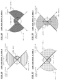
- FIGS. 4A and 4B are diagrams showing a distribution state of signal light and stray light 1 , 2 on the plane S 0 , in the case where the propagating directions of light fluxes (signal light, stray light 1 , 2 ) passing through the four areas A through D shown in FIG. 2A are respectively changed in different directions by the same angle.
- FIG. 4A is a diagram of the anamorphic lens when viewed from the optical axis direction of the anamorphic lens (the propagating direction along which laser light is entered into the anamorphic lens)
- FIG. 4B is a diagram showing a distribution state of signal light, stray light 1 , 2 on the plane S 0 .
- FIGS. 5A through 5D are diagrams showing a method for arranging sensors.
- FIG. 5A is a diagram showing light flux areas of reflected light (signal light) on a disc
- FIG. 5B is a diagram showing a distribution state of signal light on a photodetector, in the case where an anamorphic lens and a photodetector (a four-divided sensor) based on a conventional astigmatism method are respectively disposed on the arranged position of the anamorphic lens and on the plane S 0 , in the arrangement shown in FIG. 1A
- FIGS. 5C and 5D are diagrams showing a distribution state of signal light and a sensor layout based on the above principle, on the plane S 0 .
- the direction of a diffraction image (a track image) of signal light resulting from a track groove has an inclination of 45° with respect to the flat surface direction and the curved surface direction.
- FIG. 5A assuming that the direction of a track image is aligned with leftward and rightward directions, in FIGS. 5B through 5D , the direction of a track image by signal light is aligned in upward and downward directions.
- FIGS. 5A and 5B to simplify the description, a light flux is divided into eight light flux areas a through h. Further, the track image is shown by the solid line, and the beam shape in an out-of-focus state is shown by the dotted line.
- sensors P 1 through P 4 (a four-divided sensor) of a photodetector are arranged as shown in FIG. 5B .
- a focus error signal FE and a push-pull signal PP are obtained by the following equations (1) and (2).
- FE ( A+B+E+F ) ⁇ ( C+D+G+H )
- PP ( A+B+G+H ) ⁇ ( C+D+E+F ) (2)
- signal light is distributed in the signal light area as shown in FIG. 5C in the distribution state shown in FIG. 4B .
- signal light passing through the light flux areas a through h shown in FIG. 5A is distributed as shown in FIG. 5D .
- signal light passing through the light flux areas a through h in FIG. 5A are guided to the light flux areas a through h shown in FIG. 5D , on the plane S 0 where the sensors of the photodetector are disposed.
- the focal line position of stray light 1 in the flat surface direction is close to the anamorphic lens with respect to the plane S 0 (a plane where the beam spot of signal light has a shape of a least circle of confusion)
- the focal line position of stray light 2 in the curved surface direction is away from the anamorphic lens with respect to the plane S 0 .
- the distribution state of signal light, and stray light 1 , 2 is as shown in FIG. 4B , which makes it possible to keep signal light, and stray light 1 , 2 from overlapping each other on the plane S 0 .
- the advantage based on the above principle is obtained, even if the focal line position of stray light 1 in the flat surface direction comes closer to the plane S 0 than the focal line position of signal light in the curved surface direction, or even if the focal line position of stray light 2 in the curved surface direction comes closer to the plane S 0 than the focal line position of signal light in the flat surface direction.
- a spectral element H can be used to distribute signal light passing through the eight light flux areas a through h shown in FIG. 5A , on the sensor layout shown in FIG. 5D .
- FIG. 7A is a diagram showing an arrangement of the spectral element H.
- FIG. 7A is a plan view of the spectral element H when viewed from the side of the anamorphic lens shown in FIG. 1B .
- FIG. 7A also shows the flat surface direction, the curved surface direction of the anamorphic lens shown in FIG. 1B , and a direction of a track image of laser light to be entered into the spectral element H.
- the spectral element H is made of a square transparent plate, and has a stepped diffraction pattern (a diffraction hologram) on a light incident surface thereof. As shown in FIG. 7A , the light incident surface of the spectral element H is divided into four diffraction areas Ha through Hd. The spectral element H is disposed at such a position that laser light passing through the light flux areas A through D shown in FIG. 4A are respectively entered into the diffraction areas Ha through Hd. The diffraction areas Ha through Hd respectively diffract the entered laser light in the directions Da through Dd shown in FIG. 4A by the same angle by diffraction on the diffraction areas Ha through Hd.
- a diffraction hologram a stepped diffraction pattern
- FIGS. 7B through 7D are schematic diagrams showing irradiation areas, in the case where laser light passing through the eight light flux areas a through h shown in FIG. 5A is irradiated onto the sensor layout shown in FIG. 5D .
- FIG. 7B is a diagram showing a state as to how signal light is irradiated onto the sensors P 11 through P 18 , in the case where the focus position of laser light is adjusted on a target recording layer.
- FIGS. 7C , 7 D are diagrams showing states of stray light 1 and stray light 2 in the above condition.
- the irradiation areas of laser light passing through the light flux areas a through h are indicated as irradiation areas a through h in each of the drawings of FIGS. 7B through 7D .
- signal light is irradiated onto the sensors P 11 through P 18 based on the above principle.
- the sensors P 11 through P 18 are configured such that the irradiation area of signal light is sufficiently included in each of the sensors P 11 through P 18 .
- the sensor layout is configured in such a manner that four vertices of the signal light area are positioned on the inside of four vertices on the outside of the sensor layout.
- stray light 1 is irradiated onto a position adjacent to the outside of the signal light area according to the above principle.
- the irradiation area of stray light 1 is likely to overlap the sensors P 11 through P 18 .
- the irradiation area of stray light 2 is also likely to overlap the sensors P 11 through P 18 .
- the irradiation areas a, h respectively and uniformly overlap the sensors P 11 , P 12 .
- FIG. 8C although a left end of the irradiation area b and a right end of the irradiation area c are respectively deviated from the sensors P 16 , P 14 , the irradiation areas b, c respectively and uniformly overlap the sensors P 16 , P 14 .
- the irradiation areas f, g respectively and uniformly overlap the sensors P 13 , P 15
- the irradiation areas d, e respectively and uniformly overlap the sensors P 17 , P 18 .
- FIG. 8D is a diagram showing irradiation areas of signal light passing through the light flux areas a through h, in the case where the positions of the sensors P 11 through P 18 are displaced from the state shown in FIG. 8A in a direction (leftward or rightward direction) perpendicular to the direction of a track image.
- the irradiation areas are the same as those in the state shown in FIG. 8A , since the positions of the sensors P 11 through P 18 are displaced leftward, the irradiation areas in the state shown in FIG. 8D are displaced rightward within the sensors P 11 through P 18 .
- FIG. 8F is an enlarged view showing irradiation areas near the sensors P 14 , P 16 in the state shown in FIG. 8D .
- a right end of the irradiation area b lies within the sensor P 16
- a left end of the irradiation area b overlaps the sensor P 16
- a left end of the irradiation area c lies within the sensor P 14
- a right end of the irradiation area c is deviated rightward from the sensor P 14 and overlaps the sensor P 16 , unlike the state shown in FIG. 8C .
- the output signal from the sensor P 16 is increased, and the output signal from the sensor P 14 is decreased, as compared with the state shown in FIG. 8A .
- the output signal from the sensor P 15 is increased, and the output signal from the sensor P 13 is decreased, as compared with the state shown in FIG. 8A .
- the adder circuit 14 sums up output signals from the sensors P 13 , P 14 , and outputs a signal PP 2 L in accordance with the light amount of left-side signal light of upper and lower two signal light.
- the adder circuit 15 sums up output signals from the sensors P 15 , P 16 , and outputs a signal PP 2 R in accordance with the light amount of right-side signal light of upper and lower two signal light.
- the gain circuits 16 , 17 multiplies the outputs from the adder circuits 14 , 15 by gains ⁇ , ⁇ under the control of the comparator/computer 21 .
- the subtractor circuit 18 computes a difference between output signals from the gain circuits 16 , 17 , and generates a signal PP 2 based on alight amount difference in leftward or rightward direction between the upper and lower two signal light.
- the inventive example is an example, wherein the invention is applied to an optical pickup device compatible with BD, DVD and CD.
- the above principle is applied only to an optical system for BD, and a focus adjusting technology by a conventional astigmatism method and a tracking adjusting technology by a 3-beam system (an in-line system) are applied to an optical system for CD and an optical system for DVD.
- FIGS. 10A and 10B are diagrams showing an optical system of an optical pickup device in the inventive example.
- FIG. 10A is a plan view of the optical system showing a state that elements of the optical system on the disc side with respect to rise-up mirrors 114 , 115 are omitted
- FIG. 10B is a perspective side view of the optical system posterior to the rise-up mirrors 114 , 115 .
- the optical pickup device is provided with a semiconductor laser 101 , a half wave plate 102 , a diverging lens 103 , a dual wavelength laser 104 , a diffraction grating 105 , a diverging lens 106 , a complex prism 107 , a front monitor 108 , a collimator lens 109 , a driving mechanism 110 , reflection mirrors 111 , 112 , a quarter wave plate 113 , the rise-up mirrors 114 , 115 , a dual wavelength objective lens 116 , a BD objective lens 117 , a spectral element 118 , an anamorphic lens 119 , and a photodetector 120 .
- the semiconductor laser 101 emits laser light (hereinafter, called as “BD light”) for BD and having a wavelength of or about 405 nm.
- BD light laser light
- the half wave plate 102 adjusts the polarization direction of BD light.
- the diverging lens 103 adjusts the focal length of BD light to shorten the distance between the semiconductor laser 101 and the complex prism 107 .
- FIG. 10C is a diagram showing an arrangement pattern of laser elements (laser light sources) in the dual wavelength laser 104 .
- FIG. 10C is a diagram of the dual wavelength laser 104 when viewed from the beam emission side.
- CE and DE respectively indicate emission points of CD light and DVD light.
- the gap between the emission points of CD light and DVD light is represented by the symbol G.
- the gap G between the emission point CE of CD light and the emission point DE of DVD light is set to such a value as to properly irradiate DVD light onto a four-divided sensor for DVD light.
- Accommodating two light sources in one CAN as described above enables to simplify the optical system, as compared with an arrangement provided with plural CANs.
- the diffraction grating 105 separates each of CD light and DVD light into a main beam and two sub beams.
- the diffraction grating 105 is a two-step diffraction grating.
- the diffraction grating 105 is integrally formed with a half wave plate.
- the half wave plate integrally formed with the diffraction grating 105 adjusts the polarization directions of CD light and DVD light.
- the diverging lens 106 adjusts the focal lengths of CD light and DVD light to shorten the distance between the dual wavelength laser 104 and the complex prism 107 .
- the complex prism 107 is internally formed with a dichroic surface 107 a , and a Polarizing Beam Splitter (PBS) surface 107 b .
- the dichroic surface 107 a reflects BD light, and transmits CD light and DVD light.
- the semiconductor laser 101 , the dual wavelength laser 104 and the complex prism 107 are disposed at such positions that the optical axis of BD light reflected on the dichroic surface 107 a and the optical axis of CD light transmitted through the dichroic surface 107 a are aligned with each other.
- the optical axis of DVD light transmitted through the dichroic surface 107 a is displaced from the optical axes of BD light and CD light by the gap G shown in FIG. 10C .
- a part of each of BD light, CD light and DVD light is reflected on the PBS surface 107 b , and a main part thereof is transmitted through the PBS surface 107 b .
- the half wave plate 102 , and the diffraction grating 105 (and the half wave plate integrally formed with the diffraction grating 105 ) are disposed at such positions that a part of each of BD light, CD light and DVD light is reflected on the PBS surface 107 b.
- a main beam and two sub beams of CD light, and a main beam and two sub beams of DVD light are respectively aligned along the tracks of CD and DVD.
- the main beam and the two sub beams reflected on CD are irradiated onto four-divided sensors for CD on the photodetector 120 , which will be described later.
- the main beam and two sub beams reflected on DVD are irradiated onto four-divided sensors for DVD on the photodetector 120 , which will be described later.
- the front monitor 108 outputs a signal in accordance with a received light amount.
- the signal from the front monitor 108 is used for emission power control of the semiconductor laser 101 and the dual wavelength laser 104 .
- the collimator lens 109 converts BD light, CD light and DVD light entered from the side of the complex prism 107 into parallel light.
- the driving mechanism 110 moves the collimator lens 109 in the optical axis direction in accordance with a control signal for aberration correction.
- the driving mechanism 110 is provided with a holder 110 a for holding the collimator lens 109 , and a gear 110 b for feeding the holder 110 a in the optical axis direction of the collimator lens 109 .
- the gear 110 b is interconnected to a driving shaft of a motor 110 c.
- the rise-up mirror 114 is a dichroic mirror.
- the rise-up mirror 114 transmits BD light, and reflects CD light and DVD light in a direction toward the dual wavelength objective lens 116 .
- the rise-up mirror 115 reflects BD light in a direction toward the BD objective lens 117 .
- the spectral element 118 has a stepped diffraction pattern (a diffraction hologram) on an incident surface thereof. Out of BD light, CD light and DVD light entered into the spectral element 118 , BD light is divided into twelve light fluxes, which will be described later, and the propagating direction of each of the light fluxes is changed by diffraction on the spectral element 118 . Main parts of CD light and DVD light are transmitted through the spectral element 118 without diffraction on the spectral element 118 . An arrangement of the spectral element 118 will be described later referring to FIG. 11A .
- the anamorphic lens 119 imparts astigmatism to BD light, CD light and DVD light entered from the side of the spectral element 118 .
- the anamorphic lens 119 corresponds to the anamorphic lens shown in FIG. 1B .
- BD light, CD light and DVD light transmitted through the anamorphic lens 119 are entered into the photodetector 120 .
- the photodetector 120 has a sensor layout for receiving the respective light. The sensor layout of the photodetector 120 will be described later referring to FIG. 12 .
- the spectral element 118 is made of a square transparent plate, and has a stepped diffraction pattern (a diffraction hologram) on a light incident surface thereof.
- the diffraction pattern is a stepped diffraction pattern.
- the step number and the step height of the diffraction pattern are set such that plus first order diffraction efficiency with respect to the wavelength of BD light is set high, and that zero-th order diffraction efficiency with respect to the wavelengths of CD light and DVD light is set high.
- the light incident surface of the spectral element 118 is divided into sixteen diffraction areas 118 a 0 through 118 h 0 , 118 a 1 through 118 h 1 .
- the spectral element 118 is disposed at such a position that BD light is uniformly entered into each of the diffraction areas 118 a 0 through 118 h 0 , 118 a 1 through 118 h 1 .
- the spectral element 118 is disposed at such a position that the center of the spectral element 118 shown in FIG. 11A is aligned with the optical axis of BD light.
- an area (hereinafter, called as a “vertically oriented area”) obtained by combining the diffraction areas 118 a 1 , 118 d 1 , 118 e 1 , 118 h 1 extends in a direction perpendicular to the direction of a track image of laser light, and has a width d.
- An area (hereinafter, called as a “transversely oriented area”) obtained by combining the diffraction areas 118 b 1 , 118 c 1 , 118 f 1 , 118 g 1 extends in a direction in parallel to the direction of a track image of laser light, and has a width d.
- FIG. 11B is a diagram showing light flux areas a 0 through h 0 , a 1 through h 1 of BD light which is entered into the diffraction areas 118 a 0 through 118 h 0 , 118 a 1 through 118 h 1 of the spectral element 118 .
- Light passing through light flux areas a 0 through h 0 , a 1 through h 1 is respectively entered into the diffraction areas 118 a 0 through 118 h 0 , 118 a 1 through 118 h 1 .
- the diffraction areas 118 a 0 through 118 h 0 diffract entered BD light in directions Va 0 through Vh 0 by plus first order diffraction.
- the directions Va 0 , Vh 0 , the directions Vf 0 , Vg 0 , the directions Vb 0 , Vc 0 , the directions Vd 0 , Ve 0 respectively coincide with the directions Da through Dd shown in FIG. 4A .
- each of the diffraction areas 118 a 0 through 118 h 0 diffracts BD light by the same diffraction angle by plus first order diffraction.
- the diffraction angle is adjusted by the pitch of a diffraction pattern.
- the diffraction areas 118 a 1 through 118 h 1 diffract entered BD light in directions Va 1 through Vh 1 by plus first order diffraction.
- the directions Va 1 through Vh 1 are inclined by 45° with respect to the directions Va 0 through Vh 0 .
- the directions Va 1 , Vd 1 , the directions Ve 1 , Vh 1 are respectively directions in parallel to the flat surface direction and different from each other; and the directions Vb 1 , Vg 1 , the directions Vc 1 , Vf 1 are respectively directions in parallel to the curved surface direction and different from each other.
- BD light diffracted on the diffraction areas 118 a 0 through 118 h 0 is irradiated onto the light receiving surface of the photodetector 120 , as shown in FIG. 4B . Further, as will be described later, BD light diffracted on the diffraction areas 118 a 1 through 118 h 1 is irradiated onto a position on the outside of a rectangle defined by vertices on the outside of the sensor layout, on the light receiving surface of the photodetector 120 .
- CD light and DVD light are irradiated onto four-divided sensors on the photodetector 120 , which will be described later, substantially without diffraction on the diffraction areas 118 a 0 through 118 h 0 , 118 a 1 through 118 h 1 .
- the diffraction areas 118 a 0 through 118 h 0 , 118 a 1 through 118 h 1 are formed by e.g. a diffraction pattern having eight steps.
- the step difference per step is set to 7.35 ⁇ m.
- FIG. 12 is a diagram showing a sensor layout of the photodetector 120 .
- the photodetector 120 has sensors B 1 through B 8 for BD and for receiving BD light separated by the spectral element 118 ; four-divided sensors C 01 through C 03 for CD and for receiving CD light transmitted through the spectral element 118 without separation by the spectral element 118 ; and four-divided sensors D 01 through D 03 for DVD and for receiving DVD light transmitted through the spectral element 118 without separation by the spectral element 118 .
- Signal light of BD light separated by the spectral element 118 is respectively irradiated onto vertex portions of the signal light area, in the same manner as the irradiation area of signal light shown in FIG. 4B .
- the sensors B 1 , B 2 , the sensors B 3 , B 5 , the sensors B 4 , B 6 , the sensors B 7 , B 8 are respectively disposed near the four vertices of the signal light area to receive signal light of BD light passing through the light flux areas a 0 through h 0 , respectively.
- the sensors B 1 through B 8 are disposed at such positions that the irradiation area of BD light which is positioned on the inside of the four vertex portions of the signal light area is sufficiently included.
- the optical axes of BD light and CD light are aligned with each other on the dichroic surface 107 a as described above. Accordingly, a main beam (zero-th order diffraction light) of CD light is irradiated onto a center of the signal light area of BD light, on the light receiving surface of the photodetector 120 .
- the four-divided sensor C 01 is disposed at the center position of a main beam of CD light.
- the four-divided sensors C 02 , C 03 are disposed in the direction of a track image with respect to a main beam of CD light, on the light receiving surface of the photodetector 120 , to receive sub beams of CD light.
- FIGS. 13A through 13C are schematic diagrams showing irradiation areas of BD light, in the case where BD light passing through the sixteen light flux areas a 0 through h 0 , a 1 through h 1 shown in FIG. 11B is irradiated onto the sensors B 1 through B 8 shown in FIG. 12 .
- FIGS. 13A through 13C are diagrams respectively showing signal light, stray light 1 and stray light 2 of BD light that is irradiated onto the sensors B 1 through B 8 , in the case where the focus position of BD light is adjusted on a target recording layer.
- the irradiation areas of BD light passing through the light flux areas a 0 through h 0 , a 1 through h 1 are indicated as irradiation areas a 0 through h 0 , a 1 through h 1 in each of the drawings of FIGS. 13A through 13C .
- the shape of the sensors B 1 through B 8 shown in FIGS. 13A through 13C is simplified in comparison with the shape of the sensors B 1 through B 8 shown in FIG. 12 .
- signal light of BD light passing through the light flux areas a 0 through h 0 is irradiated onto the sensors B 1 through B 8
- signal light of BD light passing through the light flux areas a 1 through h 1 is irradiated onto a position away from the signal light area.
- signal light of BD light to be entered into the spectral element 118 signal light of BD light to be entered into the diffraction areas 118 a 1 through 118 h 1 is diffracted with a large diffraction angle toward the outside of the signal light area.
- the irradiation areas a 0 , h 0 , the irradiation areas b 0 , c 0 , the irradiation areas f 0 , g 0 , and the irradiation areas d 0 , e 0 each has a shape obtained by removing a center portion from a corresponding one of the four irradiation areas (see FIG. 7B ) obtained in the case where the spectral element H is used, depending on the width d shown in FIG. 11A .
- stray light 1 , 2 of BD light passing through the light flux areas a 0 through h 0 , a 1 through h 1 are irradiated onto a position on the outside of the signal light area.
- the clearance is formed depending on the width d shown in FIG. 11A .
- the irradiation areas a 0 , h 0 , the irradiation areas b 0 , c 0 , the irradiation areas f 0 , g 0 , the irradiation areas d 0 , e 0 each has a shape obtained by removing a boundary portion between the respective two irradiation areas from a corresponding one of the irradiation areas in the state shown in FIGS. 7C , 7 D obtained in the case where the spectral element H is used, by the diffraction areas 118 a 1 through 118 h 1 shown in FIG. 11A . As shown in FIGS. 13B , 13 C, these clearances extend near the vertices of the signal light area. With this arrangement, there is no or less likelihood that stray light 1 , 2 may be entered into the sensors near the vertices of the signal light area.
- FIG. 14A is a diagram showing an irradiation area of signal light passing through the light flux areas a 0 through h 0 , in the case where the positions of the sensors B 1 through B 8 are not displaced.
- FIG. 14A shows a state that the focus position of laser light is adjusted on a target recording layer.
- signal light passing through the light flux areas a 0 through h 0 is uniformly irradiated onto each of the sensors.
- FIGS. 14B , 14 C are enlarged views showing an irradiation area near the sensors B 1 , B 2 , and an irradiation area near the sensors B 4 , B 6 , respectively, in the case shown in FIG. 14A .
- the hatched portions in between the irradiation areas in FIGS. 14B , 14 C respectively indicate areas, with signal light being removed by the diffraction areas 118 a 1 , 118 h 1 , the diffraction areas 118 b 1 , 118 c 1 of the spectral element 118 .
- BD light passing through the light flux areas a, h, and the light flux areas b, c is irradiated onto areas obtained by adding the hatched portions to the broken-line portions.
- the irradiation area a 0 has a shape with an upper end of the irradiation area a shown in FIG. 8B being removed, and the irradiation area h 0 has a shape with a lower end of the irradiation area h shown in FIG. 8B being removed.
- the irradiation areas a 0 , h 0 respectively and uniformly overlap the sensors B 1 , B 2 .
- the irradiation area b 0 has a shape with a left end of the irradiation area b shown in FIG.
- the irradiation area c 0 has a shape with a right end of the irradiation area c shown in FIG. 8C being removed.
- the irradiation areas b 0 , c 0 respectively and uniformly overlap the sensors B 6 , B 4 .
- the irradiation areas f 0 , g 0 respectively and uniformly overlap the sensors B 3 , B 5
- the irradiation areas d 0 , e 0 respectively and uniformly overlap the sensors B 7 , B 8 .
- FIG. 14D is a diagram showing an irradiation area of signal light passing through the light flux areas a 0 through h 0 , in the case where the positions of the sensors B 1 through B 8 are displaced from the state shown in FIG. 14A in a direction (leftward or rightward direction) perpendicular to the direction of a track image.
- the irradiation areas are the same as those in the state shown in FIG. 14A , since the positions of the sensors B 1 through B 8 are displaced leftward, the irradiation areas in FIG. 14D are displaced rightward within the sensors B 1 through B 8 .
- FIG. 14E is an enlarged view showing irradiation areas near the sensors B 1 , B 2 in the state shown in FIG. 14D .
- the irradiation areas a 0 , h 0 respectively and uniformly overlap the sensors B 1 , B 2 in the same manner as the state shown in FIG. 14B , although the irradiation areas a 0 , h 0 are respectively shifted rightward with respect to the sensors B 1 , B 2 .
- the output signals from the sensors B 1 , B 2 in FIG. 14E are substantially the same as the output signals from the sensors B 1 , B 2 in the state shown in FIG. 14A .
- the output signals from the sensors B 7 , B 8 in FIG. 14E are substantially the same as the output signals from the sensors B 7 , B 8 in the state shown in FIG. 14A .
- FIG. 14F is an enlarged view showing irradiation areas near the sensors B 4 , B 6 in the state shown in FIG. 14D .
- the irradiation area b 0 lies within the sensor B 6 in the same manner as the state shown in FIG. 14C .
- the irradiation area c 0 lies within the sensor B 4 in the same manner as the state shown in FIG. 14C .
- the output signals from the sensors B 4 , B 6 in FIG. 14F are respectively substantially the same as the output signals from the sensors B 4 , B 6 in the state shown in FIG. 14A .
- the output signal from the sensors B 3 , B 5 in FIG. 14F are respectively substantially the same as the output signals from the sensors B 3 , B 5 in the state shown in FIG. 14A .
- the output signals from the sensors B 1 through B 8 are kept substantially unchanged in the same manner as the states shown in FIGS. 14D through 14F . Accordingly, even if the positions of the sensors B 1 through B 8 are displaced in a direction (upward or downward direction) in parallel to the direction of a track image substantially by the same displacement amount as the state shown in FIG. 14D , the output signals from the sensors B 1 through B 8 are kept substantially unchanged.
- the clearance between the respective two irradiation areas positioned at four vertex portions of the signal light area larger than the clearance between the respective two sensors corresponding to the respective two irradiation areas so as to keep the output signals from the sensors B 1 through B 8 substantially unchanged, even if the positions of the sensors B 1 through B 8 are displaced.
- the clearance between the respective two irradiation areas is properly adjusted by the width d shown in FIG. 11A .
- FIGS. 15A through 15D show simulation results of irradiation areas on the sensor layout, in the case where the spectral element H is used, and in the case where the spectral element 118 in the inventive example is used.
- FIG. 15A shows a distribution state of signal light, stray light 1 , 2 on the light receiving surface, in the case where the spectral element H shown in FIG. 7A is used, and FIG. 15B is an enlarged view of a right vertex portion in the state shown in FIG. 15A .
- FIG. 15C shows a distribution state of signal light, stray light 1 , 2 on the light receiving surface, in the case where the spectral element 118 is used, and
- FIG. 15D is an enlarged view of a right vertex portion in the state shown in FIG. 15C .
- FIGS. 15A through 15D respectively show simulation results in the case where there is no lens shift.
- FIG. 16A shows a distribution state of signal light, stray light 1 , 2 on the light receiving surface, in the case where the spectral element H is used
- FIG. 16B is an enlarged view of a right vertex portion in the state shown in FIG. 16A
- FIG. 16C shows a distribution state of signal light, stray light 1 , 2 on the light receiving surface, in the case where the spectral element 118 is used
- FIG. 16D is an enlarged view of a right vertex portion in the state shown in FIG. 16C
- FIGS. 16A through 16D respectively show simulation results in the case where a lens is shifted by 300 ⁇ m.
- the width d of the spectral element 118 is set to 10% of the diameter of laser light to be entered into the spectral element 118 . Further, the above simulation is made based on the premise that the BD objective lens 117 is not shifted in FIGS. 15A through 15D , and that the BD objective lens 117 is shifted by 300 ⁇ m in FIGS. 16A through 16D . Furthermore, in the above simulation, a light receiving sensor is constituted of the sensors B 1 through B 8 in the inventive example.
- FIGS. 15A and 15B in the case where the spectral element H is used, the irradiation area of stray light comes close to the irradiation area of signal light. As a result, stray light is likely to be entered into the sensors B 1 through B 8 . In contrast, as shown in FIGS. 15C and 15 D, FIGS.
- the inventive example there is no or less likelihood that stray light 1 , 2 may be superimposed on signal light of BD light, as compared with the case where the spectral element H is used.
- the inventive example is advantageous in enhancing the precision of output signals from the sensors B 1 through B 8 based on signal light of BD light.
- the inventive example is advantageous in enhancing the precision of output signals from the sensors B 1 through B 8 , even if the positions of the sensors B 1 through B 8 are displaced.
- the inventive example is advantageous even in the case where a positional displacement amount of the sensors B 1 through B 8 is larger than the positional displacement amount shown in FIG. 14D , and the signal light area to be formed by signal light of BD light is deviated from a rectangle defined by the vertices on the outside of the sensor layout. Specifically, in the inventive example, even in the case where positional displacement of the sensors B 1 through B 8 is large, the amount by which each of the irradiation areas is deviated from a corresponding sensor, and the amount by which each of the irradiation areas overlaps a sensor adjacent to the corresponding sensor are decreased, as compared with the case where the spectral element H is used.
- BD light is diffracted on diffraction areas adjacent to each other, out of the diffraction areas 118 a 1 through 118 h 1 , in the flat surface direction or the curved surface direction, and in directions different form each other.
- the diffraction direction may be set, as necessary, in such a manner that diffracted BD light is not irradiated onto the sensors B 1 through B 8 .
- diffraction areas adjacent to each other, out of the diffraction areas 118 a 1 through 118 h 1 may be integrally formed into one diffraction area.
- the diffraction direction may also be set, as necessary, in such a manner that diffracted BD light is not irradiated onto the sensors B 1 through B 8 .
- the vertically oriented area and the transversely oriented area having the width d are formed along straight lines inclined from the flat surface direction and from the curved surface direction by 45°.
- the vertically oriented area and the transversely oriented area may be formed with a light blocking portion where incidence of laser light is blocked.
- signal light of BD light is irradiated onto the sensors B 1 through B 8 in the same manner as the inventive example.
- the light amount of CD light to be irradiated onto the four-divided sensors C 01 through C 03 , and the light amount of DVD light to be irradiated onto the four-divided sensors D 01 through D 03 are reduced by the light blocking portions.
- the optical system for receiving BD light, and the optical system for receiving CD light and DVD light may be individually constructed.
- BD light is separated by the spectral element 118 having a diffraction pattern on a light incident surface thereof.
- BD light may be separated by using a spectral element constituted of a multifaceted prism.
- the optical system for receiving BD light and the optical system for receiving CD light and DVD light are individually constructed.
- BD light is guided to the BD objective lens 117 shown in FIG. 10B by the optical system for BD
- CD light and DVD light are guided to the dual wavelength objective lens 116 by the optical system for CD/DVD which is constructed independently of the optical system for BD.
- the optical system for BD has a laser light source for emitting BD light, and one photodetector for receiving BD light reflected on BD.
- the optical system for CD/DVD has a laser light source for emitting CD light and DVD light, and a photodetector other than the photodetector for BD light and for receiving CD light, DVD light reflected on CD, DVD.
- the photodetector for CD/DVD has two sensor groups for individually receiving CD light and DVD light.
- the optical system for BD is provided with an anamorphic lens for imparting astigmatism to BD light reflected on BD.
- the spectral element constituted of a multifaceted prism is disposed, for example, anterior to the anamorphic lens.
- FIGS. 17A , 17 B are schematic diagrams showing an arrangement of a spectral element 121 constituted of a multifaceted prism.
- FIG. 17A is a perspective view of the spectral element 121
- FIG. 17B is a plan view of the spectral element 121 when viewed from an incident surface thereof.
- the spectral element 121 is constituted of a multifaceted prism.
- Surfaces 121 a through 121 d each inclined in a direction different from the optical axis of BD light are formed on the incident surface of the spectral element 121 .
- BD light is entered into the spectral element 121 in such a manner that the optical axis of BD light is aligned with the center of the spectral element 121 . With this arrangement, BD light is uniformly entered into the surfaces 121 a through 121 d .
- BD light entered into the surfaces 121 a through 121 d is respectively refracted on the surfaces 121 a through 121 d in the directions Va through Vd, and the propagating directions of BD light are changed by the same angle.
- the directions Va through Vd coincide with the directions Da through Dd shown in FIG. 4A , respectively.
- the output surface of the spectral element 121 is formed with a light blocking portion 121 e having a width d and formed in parallel to the direction of a track image of entered light, and a light blocking portion 121 f having a width d and formed in a direction perpendicular to the direction of a track image of entered light.
- the light blocking portions 121 e , 121 f are formed by e.g. attaching a light blocking mask member on a flat output surface thereof. With this arrangement, a part of BD light to be entered into the surfaces 121 a through 121 d is blocked by the light blocking portions 121 e , 121 f .
- BD light to be entered into areas 121 a 1 , 121 a 2 within the surface 121 a , areas 121 b , 121 b 2 within the surface 121 b , areas 121 c 1 , 121 c 2 within the surface 121 c , areas 121 d 1 , 121 d 2 within the surface 121 d is not blocked by the light blocking portions 121 e , 121 f .
- the irradiation areas of signal light and stray light 1 , 2 that have been transmitted through the spectral element 121 are formed near the signal light area, as indicated by the irradiation areas a 0 through h 0 shown in FIGS. 13A through 13C .
- the irradiation areas a 1 through h 1 are not formed by light blocking by the light blocking portions 121 e , 121 f.
- the surfaces 121 a through 121 d are formed on an incident surface of the spectral element 121
- the light blocking portions 121 e , 121 f are formed on a flat output surface of the spectral element 121 .
- the surfaces 121 a through 121 d may be formed on an output surface of the spectral element 121
- the light blocking portions 121 e , 121 f may be formed on a flat incident surface of the spectral element 121 .
- a slope capable of obtaining refraction substantially equivalent to diffraction by the diffraction areas 118 a 1 through 118 h 1 of the spectral element 118 may be formed, in place of the light blocking portions 121 e , 121 f.
- the vertically oriented area and the transversely oriented area of the spectral element 118 are configured to have the width d.
- the vertically oriented area and the transversely oriented area of the spectral element 118 may be configured to have widths different from each other.
- FIG. 18A is a diagram showing an arrangement of the spectral element 118 whose vertically oriented area and transversely oriented area have widths different from each other.
- the width d′ of the vertically oriented area is set smaller than the width d of the transversely oriented area.
- a lower end of the diffraction areas 118 a 1 , 118 h 1 , and an upper end of the diffraction areas 118 d 1 , 118 e 1 have a pointed-arrow shape.
- FIG. 18B is a diagram showing light flux areas a 0 through h 0 , a 1 through h 1 of BD light that is entered into diffraction areas 118 a 0 through 118 h 0 , 118 a 1 through 118 h 1 of the modified spectral element 118 .
- the modified spectral element 118 As compared with the spectral element 118 shown in FIG. 11A , in the case where the modified spectral element 118 is used, the light flux areas a 0 , d 0 , e 0 , h 0 are increased, and the light flux areas a 1 , d 1 , e 1 , h 1 are decreased.
- the irradiation areas b 0 , c 0 , f 0 , g 0 by the spectral element 118 shown in FIG. 18A are the same as those in the state shown in FIG.
- the irradiation areas on the sensors B 1 , B 2 , B 7 , B 8 with less influence by the displacement are set larger than those in the inventive example.
- the precision of output signals from the sensors B 1 , B 2 , B 7 , B 8 are further enhanced as compared with the inventive example, while enhancing the precision of output signals from the sensors B 3 through B 6 in the same manner as the inventive example.
- the width d′ of the vertically oriented area is set smaller than the width d of the transversely oriented area
- the irradiation areas a 0 , d 0 , e 0 , h 0 are set larger than those in the state shown in FIG. 13A substantially by the same amount.
- the output signals from the sensors B 1 , B 2 , B 7 , B 8 are also increased as compared with the state shown in FIG. 13A substantially by the same amount.
- the spectral element 118 in such a manner that the width of the transversely oriented area is set larger than the width of the vertically oriented area. Further, in the case where the sensors B 1 through B 8 are likely to be greatly displaced in the direction of a track image resulting from e.g. aging deterioration, it is desirable to configure the spectral element 118 in such a manner that the width of the vertically oriented area is set larger than the width of the transversely oriented area. Furthermore, it is desirable to properly set the widths of the vertically oriented area and the transversely oriented area, in accordance with on a direction in which the sensors B 1 through B 8 are likely to be displaced.
- the width of the transversely oriented area or of the vertically oriented area may be set to zero.
- FIG. 19A is a diagram showing an arrangement of a spectral element 122 , in the case where the width of the vertically oriented area of the spectral element 118 is set to zero.
- the spectral element 122 is formed with diffraction areas 122 a through 122 h .
- an area (a transversely oriented area) formed by combining the diffraction areas 122 g , 112 h has the width d.
- BD light passing through light flux areas a 2 through h 2 is respectively entered into the diffraction areas 122 a through 122 h of the spectral element 122 .
- the irradiation areas by the light flux areas b 2 , c 2 , e 2 , f 2 are respectively coincident with the irradiation areas b 0 , c 0 , f 0 , g 0 shown in FIG. 13A .
- signal light of BD light passing through the light flux areas a 2 , d 2 is respectively irradiated onto parts of the sensors B 1 , B 2 , and onto parts of the sensors B 7 , B 8 in the same manner as the case where the spectral element H is used.
- the precision of output signals from the sensors B 3 through B 6 are enhanced in the same manner as the inventive example. Further, since the irradiation areas on the sensors B 1 , B 2 , B 7 , B 8 are increased, the precision of output signals from the sensors B 1 , B 2 , B 7 , B 8 are further enhanced, as compared with the inventive example.
- output signals from the sensors B 1 , B 2 , B 7 , B 8 are also increased substantially by the same amount, in the same manner as the case where the spectral element 118 shown in FIG. 18A is used.
- the increased amounts of output signals are offset with each other in the equations (1), (2), there is no likelihood that such an increase may affect the focus error signal FE and the push-pull signal PP.
- the spectral element 118 in such a manner that the width of the vertically oriented area is set to zero. Further, in the case where the positions of the sensors B 1 through B 8 are greatly displaced only in the direction of a track image resulting from e.g. aging deterioration, it is desirable to configure the spectral element 118 in such a manner that the width of the transversely oriented area is set to zero.
- the spectral element 118 is disposed anterior to the anamorphic lens 119 .
- the spectral element 118 may be disposed posterior to the anamorphic lens 119 , or a diffraction pattern for imparting the same diffraction function as the spectral element 118 to laser light may be integrally formed on an incident surface or an output surface of the anamorphic lens 119 .
Landscapes
- Physics & Mathematics (AREA)
- Optics & Photonics (AREA)
- Optical Head (AREA)
- Optical Recording Or Reproduction (AREA)
Abstract
Description
FE=(A+B+E+F)−(C+D+G+H) (1)
PP=(A+B+G+H)−(C+D+E+F) (2)
α={(PP2L+PP2R)/2}/PP2L (3)
β={(PP2L+PP2R)/2}/PP2R (4)
Claims (7)
Applications Claiming Priority (2)
| Application Number | Priority Date | Filing Date | Title |
|---|---|---|---|
| JP2010-172210 | 2010-07-30 | ||
| JP2010172210A JP2012033231A (en) | 2010-07-30 | 2010-07-30 | Optical pickup device |
Publications (2)
| Publication Number | Publication Date |
|---|---|
| US20120026857A1 US20120026857A1 (en) | 2012-02-02 |
| US8331211B2 true US8331211B2 (en) | 2012-12-11 |
Family
ID=45526613
Family Applications (1)
| Application Number | Title | Priority Date | Filing Date |
|---|---|---|---|
| US13/186,833 Expired - Fee Related US8331211B2 (en) | 2010-07-30 | 2011-07-20 | Optical pickup device |
Country Status (3)
| Country | Link |
|---|---|
| US (1) | US8331211B2 (en) |
| JP (1) | JP2012033231A (en) |
| CN (1) | CN102347035A (en) |
Families Citing this family (1)
| Publication number | Priority date | Publication date | Assignee | Title |
|---|---|---|---|---|
| CN105487237B (en) * | 2015-12-29 | 2018-06-12 | 大连楼兰科技股份有限公司 | Optical splitting element, device and method of a multi-beam laser radar |
Citations (16)
| Publication number | Priority date | Publication date | Assignee | Title |
|---|---|---|---|---|
| US20020048233A1 (en) * | 2000-09-07 | 2002-04-25 | Masakazu Ogasawara | Optical pickup device and focus error detecting method therefor |
| JP2006073042A (en) | 2004-08-31 | 2006-03-16 | Asahi Glass Co Ltd | Diffraction element and optical head device |
| US20090201787A1 (en) * | 2006-07-13 | 2009-08-13 | Pioneer Corporation | Pickup device |
| US20090225645A1 (en) | 2008-03-04 | 2009-09-10 | Sanyo Electric Co., Ltd. | Optical pickup apparatus and focal-point adjusting method |
| US20090278029A1 (en) * | 2006-11-01 | 2009-11-12 | Pioneer Corporation | Pickup device |
| US20100027404A1 (en) * | 2008-07-31 | 2010-02-04 | Sanyo Electric Co., Ltd. | Optical pickup apparatus and focal-point adjusting method |
| US20100027405A1 (en) * | 2008-08-01 | 2010-02-04 | Sanyo Electric Co., Ltd. | Optical pickup apparatus, focal-point adjusting method, and optical disc apparatus |
| US20100027386A1 (en) * | 2008-08-01 | 2010-02-04 | Sanyo Electric Co., Ltd. | Optical pickup apparatus, focal-point adjusting method, and optical disc apparatus |
| US20100080106A1 (en) | 2008-09-29 | 2010-04-01 | Sanyo Electric Co., Ltd. | Optical pickup apparatus and optical disc apparatus |
| US20100177619A1 (en) * | 2006-10-04 | 2010-07-15 | Pioneer Corporation | Pickup device |
| US20100182891A1 (en) | 2009-01-20 | 2010-07-22 | Sanyo Electric Co., Ltd. | Optical pickup device and optical disc device |
| US20100271926A1 (en) * | 2009-04-28 | 2010-10-28 | Sanyo Electric Co., Ltd. | Optical pickup device and optical disc device |
| US20100329102A1 (en) * | 2009-06-25 | 2010-12-30 | Sanyo Electric Co., Ltd. | Optical pickup device |
| US20110026382A1 (en) * | 2009-07-29 | 2011-02-03 | Sanyo Electric Co., Ltd. | Optical pickup device, optical disc device and focus adjusting method |
| US20110075545A1 (en) * | 2009-09-28 | 2011-03-31 | Sanyo Electric Co., Ltd. | Optical pickup device |
| US20110075544A1 (en) * | 2009-09-28 | 2011-03-31 | Sanyo Electric Co., Ltd. | Optical pickup device |
-
2010
- 2010-07-30 JP JP2010172210A patent/JP2012033231A/en active Pending
-
2011
- 2011-05-31 CN CN2011101574705A patent/CN102347035A/en active Pending
- 2011-07-20 US US13/186,833 patent/US8331211B2/en not_active Expired - Fee Related
Patent Citations (19)
| Publication number | Priority date | Publication date | Assignee | Title |
|---|---|---|---|---|
| US20020048233A1 (en) * | 2000-09-07 | 2002-04-25 | Masakazu Ogasawara | Optical pickup device and focus error detecting method therefor |
| JP2006073042A (en) | 2004-08-31 | 2006-03-16 | Asahi Glass Co Ltd | Diffraction element and optical head device |
| US20090201787A1 (en) * | 2006-07-13 | 2009-08-13 | Pioneer Corporation | Pickup device |
| US20100177619A1 (en) * | 2006-10-04 | 2010-07-15 | Pioneer Corporation | Pickup device |
| US20090278029A1 (en) * | 2006-11-01 | 2009-11-12 | Pioneer Corporation | Pickup device |
| US20090225645A1 (en) | 2008-03-04 | 2009-09-10 | Sanyo Electric Co., Ltd. | Optical pickup apparatus and focal-point adjusting method |
| JP2009211770A (en) | 2008-03-04 | 2009-09-17 | Sanyo Electric Co Ltd | Optical pickup device and focus adjusting method |
| US20100027404A1 (en) * | 2008-07-31 | 2010-02-04 | Sanyo Electric Co., Ltd. | Optical pickup apparatus and focal-point adjusting method |
| US20100027386A1 (en) * | 2008-08-01 | 2010-02-04 | Sanyo Electric Co., Ltd. | Optical pickup apparatus, focal-point adjusting method, and optical disc apparatus |
| US20100027405A1 (en) * | 2008-08-01 | 2010-02-04 | Sanyo Electric Co., Ltd. | Optical pickup apparatus, focal-point adjusting method, and optical disc apparatus |
| US20100080106A1 (en) | 2008-09-29 | 2010-04-01 | Sanyo Electric Co., Ltd. | Optical pickup apparatus and optical disc apparatus |
| JP2010102813A (en) | 2008-09-29 | 2010-05-06 | Sanyo Electric Co Ltd | Optical pickup apparatus and optical disk apparatus |
| US20100182891A1 (en) | 2009-01-20 | 2010-07-22 | Sanyo Electric Co., Ltd. | Optical pickup device and optical disc device |
| JP2010170598A (en) | 2009-01-20 | 2010-08-05 | Sanyo Electric Co Ltd | Optical pickup device and optical disk device |
| US20100271926A1 (en) * | 2009-04-28 | 2010-10-28 | Sanyo Electric Co., Ltd. | Optical pickup device and optical disc device |
| US20100329102A1 (en) * | 2009-06-25 | 2010-12-30 | Sanyo Electric Co., Ltd. | Optical pickup device |
| US20110026382A1 (en) * | 2009-07-29 | 2011-02-03 | Sanyo Electric Co., Ltd. | Optical pickup device, optical disc device and focus adjusting method |
| US20110075545A1 (en) * | 2009-09-28 | 2011-03-31 | Sanyo Electric Co., Ltd. | Optical pickup device |
| US20110075544A1 (en) * | 2009-09-28 | 2011-03-31 | Sanyo Electric Co., Ltd. | Optical pickup device |
Also Published As
| Publication number | Publication date |
|---|---|
| US20120026857A1 (en) | 2012-02-02 |
| CN102347035A (en) | 2012-02-08 |
| JP2012033231A (en) | 2012-02-16 |
Similar Documents
| Publication | Publication Date | Title |
|---|---|---|
| JP4610628B2 (en) | Optical pickup device and focus adjustment method | |
| JP4610662B2 (en) | Optical pickup device and optical disk device | |
| US8270280B2 (en) | Optical pickup device | |
| US8159907B2 (en) | Optical pickup device | |
| US8228778B2 (en) | Optical pickup device and optical disc device | |
| US8427922B2 (en) | Optical pickup device and optical disc device | |
| US8446809B2 (en) | Optical pickup device and optical disc device | |
| US8310910B2 (en) | Optical pickup device | |
| JP5173899B2 (en) | Optical pickup device | |
| US8264938B2 (en) | Optical pickup device | |
| US8345528B2 (en) | Optical pickup device | |
| US8331211B2 (en) | Optical pickup device | |
| US8400901B2 (en) | Optical pickup device | |
| US8325580B2 (en) | Optical pickup device | |
| US8264937B2 (en) | Optical pickup device | |
| US8432783B2 (en) | Optical pickup device and position adjusting method for light separating element | |
| US8358571B2 (en) | Optical pickup device | |
| US20120099414A1 (en) | Optical pickup device | |
| US20120106312A1 (en) | Optical pickup device | |
| JP2010049758A (en) | Optical pickup device | |
| JP2014089777A (en) | Optical pickup device |
Legal Events
| Date | Code | Title | Description |
|---|---|---|---|
| AS | Assignment |
Owner name: SANYO ELECTRIC CO., LTD., JAPAN Free format text: ASSIGNMENT OF ASSIGNORS INTEREST;ASSIGNORS:NAGATOMI, KENJI;KASAHARA, SHINSEI;SHIRANE, SHIGEHARU;AND OTHERS;SIGNING DATES FROM 20110610 TO 20110614;REEL/FRAME:026622/0262 |
|
| FEPP | Fee payment procedure |
Free format text: PAYOR NUMBER ASSIGNED (ORIGINAL EVENT CODE: ASPN); ENTITY STATUS OF PATENT OWNER: LARGE ENTITY |
|
| REMI | Maintenance fee reminder mailed | ||
| LAPS | Lapse for failure to pay maintenance fees | ||
| STCH | Information on status: patent discontinuation |
Free format text: PATENT EXPIRED DUE TO NONPAYMENT OF MAINTENANCE FEES UNDER 37 CFR 1.362 |
|
| STCH | Information on status: patent discontinuation |
Free format text: PATENT EXPIRED DUE TO NONPAYMENT OF MAINTENANCE FEES UNDER 37 CFR 1.362 |
|
| FP | Lapsed due to failure to pay maintenance fee |
Effective date: 20161211 |