US8324948B1 - Method and apparatus for duty-cycle correction with reduced current consumption - Google Patents
Method and apparatus for duty-cycle correction with reduced current consumption Download PDFInfo
- Publication number
- US8324948B1 US8324948B1 US12/889,254 US88925410A US8324948B1 US 8324948 B1 US8324948 B1 US 8324948B1 US 88925410 A US88925410 A US 88925410A US 8324948 B1 US8324948 B1 US 8324948B1
- Authority
- US
- United States
- Prior art keywords
- output
- input
- transmission gate
- coupled
- duty cycle
- Prior art date
- Legal status (The legal status is an assumption and is not a legal conclusion. Google has not performed a legal analysis and makes no representation as to the accuracy of the status listed.)
- Active, expires
Links
- 238000000034 method Methods 0.000 title claims abstract description 44
- 238000012937 correction Methods 0.000 title claims abstract description 37
- 230000005540 biological transmission Effects 0.000 claims description 45
- 239000003990 capacitor Substances 0.000 claims description 22
- 238000012935 Averaging Methods 0.000 claims description 5
- 230000015654 memory Effects 0.000 description 11
- 238000010586 diagram Methods 0.000 description 6
- 230000014509 gene expression Effects 0.000 description 5
- 230000003287 optical effect Effects 0.000 description 5
- 238000012545 processing Methods 0.000 description 5
- 238000013461 design Methods 0.000 description 4
- 230000009471 action Effects 0.000 description 3
- 230000005291 magnetic effect Effects 0.000 description 3
- 238000013459 approach Methods 0.000 description 2
- 238000004590 computer program Methods 0.000 description 2
- 230000007246 mechanism Effects 0.000 description 2
- 238000004088 simulation Methods 0.000 description 2
- 239000000654 additive Substances 0.000 description 1
- 230000000996 additive effect Effects 0.000 description 1
- 239000000835 fiber Substances 0.000 description 1
- 230000006870 function Effects 0.000 description 1
- 238000010438 heat treatment Methods 0.000 description 1
- 230000010354 integration Effects 0.000 description 1
- 230000003071 parasitic effect Effects 0.000 description 1
- 230000002093 peripheral effect Effects 0.000 description 1
- 230000008569 process Effects 0.000 description 1
- 230000000644 propagated effect Effects 0.000 description 1
- 230000008707 rearrangement Effects 0.000 description 1
- 230000009467 reduction Effects 0.000 description 1
- 239000000126 substance Substances 0.000 description 1
- 230000000007 visual effect Effects 0.000 description 1
Images


Classifications
-
- H—ELECTRICITY
- H03—ELECTRONIC CIRCUITRY
- H03K—PULSE TECHNIQUE
- H03K5/00—Manipulating of pulses not covered by one of the other main groups of this subclass
- H03K5/01—Shaping pulses
- H03K5/04—Shaping pulses by increasing duration; by decreasing duration
- H03K5/05—Shaping pulses by increasing duration; by decreasing duration by the use of clock signals or other time reference signals
Definitions
- the present invention pertains to duty-cycle (also denoted duty cycle) correction. More particularly, the present invention relates to a method and apparatus for duty-cycle correction with reduced current consumption.
- Digital circuits often produce duty cycles that are not what are needed by circuits that follow. For example, a circuit may work optimally (best performance, fastest speed, lowest power, etc.) when fed a signal having a duty cycle of 50:50 (e.g. 50% low, 50% high). If a signal has a duty cycle that is not optimal then a duty-cycle correction (DCC) circuit may be employed to correct the duty-cycle. Power consumption leads to heating and reduced reliability of a product. This presents a problem. Thus there is a great need for this technical problem to be solved by correcting the duty-cycle at reduced current consumption.
- DCC duty-cycle correction
- FIG. 1 illustrates a network environment in which the method and apparatus of the invention may be implemented
- FIG. 2 is a block diagram of a computer system in which some embodiments of the invention may be used;
- FIG. 3 illustrates one embodiment of the invention showing a schematic
- FIG. 4 illustrates one embodiment of the invention showing a schematic for a CML to CMOS converter
- FIG. 5 illustrates one embodiment of the invention showing a schematic for a reference
- FIG. 6 illustrates an analog pass gate as used in embodiments of the invention
- FIG. 7 illustrates one embodiment of the invention showing a duty cycle correction for ⁇ 5% input duty cycle distortion
- FIG. 8 illustrates, generally at 800 , one embodiment of the invention showing a duty cycle correction for +5% input duty cycle distortion
- FIG. 9 illustrates simulation results for current consumption.
- FIG. 10 illustrates various embodiments of the invention.
- current consumption in the DCC feedback block is greatly reduced over existing solutions.
- DCC loading on duty error signals (e.g. DCERR/DCERRB 314 / 316 as illustrated in FIG. 3 ) is vastly reduced over existing solutions.
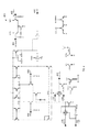
- FIG. 3 illustrates, generally at 300 , one embodiment of the invention showing a schematic.
- the instance IOUTREF 302 produces a bias voltage at 304 IREF50U.
- Instance IPHSPLIT 306 is a phase splitter.
- Instance ICML2CMOSDCC 308 is a CML-to-CMOS converter DCC.
- the outputs FBCLK 310 and FBCLKB 312 of the IPHSPLIT 306 are passed through RC time constants—averaging the signals FBCLK 310 and FBCLKB 312 and thereby generating duty-cycle error signals DCCERR 314 and DCCERRB 316 which go into ICML2CMOSDCC 308 .
- the RC time constants has as components resistors at 318 and 320 and their associated capacitance, and transmission gates 322 and 324 and their associated resistance and capacitance. For example, in FIG. 6 is shown in more detail a transmission gate. Also associated with the RC time constants are any parasitic capacitance and resistance due to component placement and/or routing and connections to other circuits.
- FIG. 4 illustrates, generally at 400 , one embodiment of the invention showing a schematic for a CML to CMOS converter such as shown in FIG. 3 at instance ICML2CMOSDCC 308 .
- DCCERRB At 402 is input DCCERRB.
- DCCERR At 406 is input INN.
- INP At 408 is input INP.
- INP At 410 is output OUT.
- At 412 is output VBNFILT.
- At 414 is input RSTBX.
- At 416 is input RSTB.
- At 418 is input IREF50U.
- At 420 is input PDB.
- FIG. 5 illustrates, generally at 500 , one embodiment of the invention showing a schematic for a reference such as shown at instance IVREF in FIG. 3 .
- a power supply (denoted VDD) VDD/2 voltage generator outputs VREF at 502 .
- PDB input PDB.
- RSTB input RSTB.
- RSTBX input RSTBX.
- EN output EN and at 512 is output ENB.
- FIG. 6 illustrates, generally at 600 , an analog pass gate as used in embodiments of the invention (e.g. FIG. 3 , etc.).
- S a source for transistor MP 1 604 and transistor MN 1 606 .
- D a drain for transistor MP 1 604 and transistor MN 1 606 .
- At 610 is CW a capacitance.
- At 612 and 614 are the control for transistor MP 1 604 and transistor MN 1 606 respectively.
- FIG. 7 illustrates, generally at 700 , one embodiment of the invention showing a duty cycle correction for ⁇ 5% input duty cycle distortion (at 706 ).
- graph 702 are shown an input duty voltage 706 and an output duty voltage 708 .
- graph 704 is a time scale for a control signal (e.g. RSTB as shown in the Figures).
- a control signal e.g. RSTB as shown in the Figures.
- the control signal e.g. RSTB as shown in the Figures
- the output voltage for correction 708 Prior to 1 ⁇ s shown on graph 704 , when the control signal (e.g. RSTB as shown in the Figures) is low the output voltage for correction 708 is below the 706 line.
- the control signal e.g. RSTB as shown in the Figures
- the output voltage for correction 708 is above the 706 line indicating a correction toward a duty cycle of 50%.
- FIG. 8 illustrates, generally at 800 , one embodiment of the invention showing a duty cycle correction for +5% input duty cycle distortion (at 806 ).
- graph 802 are shown an input duty voltage 806 and an output duty voltage 808 .
- graph 804 is a time scale for a control signal (e.g. RSTB as shown in the Figures).
- a control signal e.g. RSTB as shown in the Figures.
- the control signal e.g. RSTB as shown in the Figures
- the output voltage for correction 808 Prior to 1 ⁇ s shown on graph 804 , when the control signal (e.g. RSTB as shown in the Figures) is low the output voltage for correction 808 is above the 806 line.
- the control signal e.g. RSTB as shown in the Figures
- the output voltage for correction 808 is below the 806 line indicating a correction toward a duty cycle of 50%.
- FIG. 9 illustrates, generally at 900 , one embodiment of the invention 904 showing a simulation result for current consumption for an existing DCC design at 902 and for a DCC design using the techniques disclosed 904 .
- the average current for an existing design 902 between time 600 ns-800 ns is 1,407.7 ⁇ A
- the average current for a DCC design using the techniques disclosed 904 between time 1.2 ⁇ s ⁇ 1.4 ⁇ s is 1,133.0 ⁇ A, which represents a 19.5% reduction in current consumption.
- FIG. 10 illustrates, generally at 1000 , embodiments of the invention.
- a method for duty cycle correction comprising: receiving an output signal;
- phase splitting said output signal producing phase split signals
- At 1002 is 2. The method of claim 1 wherein said resistor-capacitor network further comprises a first transmission gate and a second transmission gate.
- At 1003 is 3. The method of claim 2 wherein said first transmission gate has an input coupled to said resistor-capacitor network and an output coupled to a correction circuit input.
- At 1006 is 6.
- the method of claim 5 further comprising a switch which when activated sets said two outputs from said resistor-capacitor network to a same voltage.
- An apparatus comprising:
- a duty cycle correction circuit having an output, a first duty cycle correction input, and a second duty cycle correction input
- phase splitter having an input, a first output, and a second output, said phase splitter input coupled to said duty cycle correction circuit output;
- a first resistor-capacitor network having an input and an output, said first resistor-capacitor network input coupled to said phase splitter first output;
- a second resistor-capacitor network having an input and an output, said second resistor-capacitor network input coupled to said phase splitter second output.
- a first transmission gate having an input and an output, said first transmission gate input coupled to said first resistor-capacitor network output;
- a second transmission gate having an input and an output, said second transmission gate input coupled to said second resistor-capacitor network output.
- a third transmission gate having an input and an output, said third transmission gate output coupled to said first transmission gate output;
- a fourth transmission gate having an input and an output, said fourth transmission gate output coupled to said second transmission gate output.
- the apparatus of claim 12 further comprising:
- a method comprising:
- FIG. 1 illustrates a network environment 100 in which the techniques described may be applied.
- the network environment 100 has a network 102 that connects S servers 104 - 1 through 104 -S, and C clients 108 - 1 through 108 -C. More details are described below.
- FIG. 2 is a block diagram of a computer system 200 in which some embodiments of the invention may be used and which may be representative of use in any of the clients and/or servers shown in FIG. 1 , as well as, devices, clients, and servers in other Figures. More details are described below.
- FIG. 1 illustrates a network environment 100 in which the techniques described may be applied.
- the network environment 100 has a network 102 that connects S servers 104 - 1 through 104 -S, and C clients 108 - 1 through 108 -C.
- S servers 104 - 1 through 104 -S and C clients 108 - 1 through 108 -C are connected to each other via a network 102 , which may be, for example, a corporate based network.
- the network 102 might be or include one or more of: the Internet, a Local Area Network (LAN), Wide Area Network (WAN), satellite link, fiber network, cable network, or a combination of these and/or others.
- LAN Local Area Network
- WAN Wide Area Network
- satellite link fiber network
- cable network or a combination of these and/or others.
- the servers may represent, for example, disk storage systems alone or storage and computing resources.
- the clients may have computing, storage, and viewing capabilities.
- the method and apparatus described herein may be applied to essentially any type of visual communicating means or device whether local or remote, such as a LAN, a WAN, a system bus, etc.
- the invention may find application at both the S servers 104 - 1 through 104 -S, and C clients 108 - 1 through 108 -C.
- FIG. 2 illustrates a computer system 200 in block diagram form, which may be representative of any of the clients and/or servers shown in FIG. 1 .
- the block diagram is a high level conceptual representation and may be implemented in a variety of ways and by various architectures.
- Bus system 202 interconnects a Central Processing Unit (CPU) 204 , Read Only Memory (ROM) 206 , Random Access Memory (RAM) 208 , storage 210 , display 220 , audio, 222 , keyboard 224 , pointer 226 , miscellaneous input/output (I/O) devices 228 via link 229 , and communications 230 via link 232 .
- CPU Central Processing Unit
- ROM Read Only Memory
- RAM Random Access Memory
- the bus system 202 may be for example, one or more of such buses as a system bus, Peripheral Component Interconnect (PCI), Advanced Graphics Port (AGP), Small Computer System Interface (SCSI), Institute of Electrical and Electronics Engineers (IEEE) standard number 1394 (FireWire), Universal Serial Bus (USB), etc.
- the CPU 204 may be a single, multiple, or even a distributed computing resource.
- Storage 210 may be Compact Disc (CD), Digital Versatile Disk (DVD), hard disks (HD), optical disks, tape, flash, memory sticks, video recorders, etc.
- Display 220 might be, for example, an embodiment of the present invention.
- the computer system may include some, all, more, or a rearrangement of components in the block diagram.
- a thin client might consist of a wireless hand held device that lacks, for example, a traditional keyboard.
- An apparatus for performing the operations herein can implement the present invention.
- This apparatus may be specially constructed for the required purposes, or it may comprise a general-purpose computer, selectively activated or reconfigured by a computer program stored in the computer.
- a computer program may be stored in a computer readable storage medium, such as, but not limited to, any type of disk including floppy disks, hard disks, optical disks, compact disk-read only memories (CD-ROMs), and magnetic-optical disks, read-only memories (ROMs), random access memories (RAMs), electrically programmable read-only memories (EPROM)s, electrically erasable programmable read-only memories (EEPROMs), FLASH memories, magnetic or optical cards, etc., or any type of media suitable for storing electronic instructions either local to the computer or remote to the computer.
- ROMs read-only memories
- RAMs random access memories
- EPROM electrically programmable read-only memories
- EEPROMs electrically erasable programmable read-only memories
- the methods of the invention may be implemented using computer software. If written in a programming language conforming to a recognized standard, sequences of instructions designed to implement the methods can be compiled for execution on a variety of hardware platforms and for interface to a variety of operating systems.
- the present invention is not described with reference to any particular programming language. It will be appreciated that a variety of programming languages may be used to implement the teachings of the invention as described herein.
- a machine-readable medium is understood to include any mechanism for storing or transmitting information in a form readable by a machine (e.g., a computer).
- a machine-readable medium includes read only memory (ROM); random access memory (RAM); magnetic disk storage media; optical storage media; flash memory devices; electrical, optical, acoustical or other form of propagated signals which upon reception causes movement in matter (e.g. electrons, atoms, etc.) (e.g., carrier waves, infrared signals, digital signals, etc.); etc.
- one embodiment or “an embodiment” or similar phrases means that the feature(s) being described are included in at least one embodiment of the invention. References to “one embodiment” in this description do not necessarily refer to the same embodiment; however, neither are such embodiments mutually exclusive. Nor does “one embodiment” imply that there is but a single embodiment of the invention. For example, a feature, structure, act, etc. described in “one embodiment” may also be included in other embodiments. Thus, the invention may include a variety of combinations and/or integrations of the embodiments described herein.
Landscapes
- Physics & Mathematics (AREA)
- Nonlinear Science (AREA)
- Logic Circuits (AREA)
Abstract
Description
Claims (14)
Priority Applications (1)
| Application Number | Priority Date | Filing Date | Title |
|---|---|---|---|
| US12/889,254 US8324948B1 (en) | 2010-09-23 | 2010-09-23 | Method and apparatus for duty-cycle correction with reduced current consumption |
Applications Claiming Priority (1)
| Application Number | Priority Date | Filing Date | Title |
|---|---|---|---|
| US12/889,254 US8324948B1 (en) | 2010-09-23 | 2010-09-23 | Method and apparatus for duty-cycle correction with reduced current consumption |
Publications (1)
| Publication Number | Publication Date |
|---|---|
| US8324948B1 true US8324948B1 (en) | 2012-12-04 |
Family
ID=47226703
Family Applications (1)
| Application Number | Title | Priority Date | Filing Date |
|---|---|---|---|
| US12/889,254 Active 2030-12-01 US8324948B1 (en) | 2010-09-23 | 2010-09-23 | Method and apparatus for duty-cycle correction with reduced current consumption |
Country Status (1)
| Country | Link |
|---|---|
| US (1) | US8324948B1 (en) |
Citations (5)
| Publication number | Priority date | Publication date | Assignee | Title |
|---|---|---|---|---|
| US5945857A (en) * | 1998-02-13 | 1999-08-31 | Lucent Technologies, Inc. | Method and apparatus for duty-cycle correction |
| US6721232B2 (en) * | 2001-12-19 | 2004-04-13 | Renesas Technology Corp. | Semiconductor device having phase error improved DLL circuit mounted thereon |
| US20070159224A1 (en) * | 2005-12-21 | 2007-07-12 | Amar Dwarka | Duty-cycle correction circuit for differential clocking |
| US7282978B2 (en) * | 2005-06-30 | 2007-10-16 | Hynix Semiconducter Inc. | Duty cycle correction device |
| US7317341B2 (en) * | 2005-09-29 | 2008-01-08 | Hynix Semiconductor, Inc. | Duty correction device |
-
2010
- 2010-09-23 US US12/889,254 patent/US8324948B1/en active Active
Patent Citations (5)
| Publication number | Priority date | Publication date | Assignee | Title |
|---|---|---|---|---|
| US5945857A (en) * | 1998-02-13 | 1999-08-31 | Lucent Technologies, Inc. | Method and apparatus for duty-cycle correction |
| US6721232B2 (en) * | 2001-12-19 | 2004-04-13 | Renesas Technology Corp. | Semiconductor device having phase error improved DLL circuit mounted thereon |
| US7282978B2 (en) * | 2005-06-30 | 2007-10-16 | Hynix Semiconducter Inc. | Duty cycle correction device |
| US7317341B2 (en) * | 2005-09-29 | 2008-01-08 | Hynix Semiconductor, Inc. | Duty correction device |
| US20070159224A1 (en) * | 2005-12-21 | 2007-07-12 | Amar Dwarka | Duty-cycle correction circuit for differential clocking |
Similar Documents
| Publication | Publication Date | Title |
|---|---|---|
| US10284188B1 (en) | Delay based comparator | |
| US9306547B2 (en) | Duty cycle adjustment with error resiliency | |
| US9490805B2 (en) | Low power driver with programmable output impedance | |
| Kutre et al. | Advanced architecture of analog to digital converter derived from half flash ADC | |
| US20230114988A1 (en) | Clock data recovery circuit and apparatus including the same | |
| US20030063677A1 (en) | Multi-level coding for digital communication | |
| US9831886B2 (en) | Background calibration for digital-to-analog converters | |
| US9130519B1 (en) | Method and apparatus for combined linear, low-noise buffer and sampler for ADC | |
| US7425856B2 (en) | Phase interpolator with output amplitude correction | |
| US20140266306A1 (en) | High speed dynamic latch | |
| US10534670B2 (en) | Electronic device with automatic and stable system restart function | |
| US8324948B1 (en) | Method and apparatus for duty-cycle correction with reduced current consumption | |
| CN107800427A (en) | Clock data recovery module | |
| US9203411B2 (en) | Compact low power level shifter for dual rail | |
| US11509327B2 (en) | System and method to enhance noise performance in a delta sigma converter | |
| US7834708B1 (en) | Method and apparatus for analog smooth switch in VCO loading control | |
| US8680910B1 (en) | Method and apparatus for glitch-free switching of multiple phase clock | |
| US8410813B2 (en) | Method and apparatus for a low power AC On-Die-Termination (ODT) circuit | |
| US11025237B1 (en) | Zero static high-speed, low power level shifter | |
| US8513992B1 (en) | Method and apparatus for implementation of PLL minimum frequency via voltage comparison | |
| US20220166413A1 (en) | Comparator set-reset latch circuit and method for capacitively storing bits | |
| JP2025516776A (en) | High speed TX topology with supply controlled serialization stage embedded in PMOS output stage - Patents.com | |
| US7741897B1 (en) | Method and apparatus for self gate pumped NMOS high speed switch | |
| US9500707B1 (en) | Method and apparatus for using tester channel as device power supply | |
| US7268599B1 (en) | Method and apparatus for buffer with programmable skew |
Legal Events
| Date | Code | Title | Description |
|---|---|---|---|
| AS | Assignment |
Owner name: INTEGRATED DEVICE TECHNOLOGY, INC., CALIFORNIA Free format text: ASSIGNMENT OF ASSIGNORS INTEREST;ASSIGNOR:MAJUMDER, AMIT;REEL/FRAME:025088/0985 Effective date: 20100922 |
|
| FEPP | Fee payment procedure |
Free format text: PAYOR NUMBER ASSIGNED (ORIGINAL EVENT CODE: ASPN); ENTITY STATUS OF PATENT OWNER: LARGE ENTITY |
|
| STCF | Information on status: patent grant |
Free format text: PATENTED CASE |
|
| FPAY | Fee payment |
Year of fee payment: 4 |
|
| AS | Assignment |
Owner name: JPMORGAN CHASE BANK, N.A., AS COLLATERAL AGENT, NE Free format text: SECURITY AGREEMENT;ASSIGNORS:INTEGRATED DEVICE TECHNOLOGY, INC.;GIGPEAK, INC.;MAGNUM SEMICONDUCTOR, INC.;AND OTHERS;REEL/FRAME:042166/0431 Effective date: 20170404 Owner name: JPMORGAN CHASE BANK, N.A., AS COLLATERAL AGENT, NEW YORK Free format text: SECURITY AGREEMENT;ASSIGNORS:INTEGRATED DEVICE TECHNOLOGY, INC.;GIGPEAK, INC.;MAGNUM SEMICONDUCTOR, INC.;AND OTHERS;REEL/FRAME:042166/0431 Effective date: 20170404 |
|
| AS | Assignment |
Owner name: GIGPEAK, INC., CALIFORNIA Free format text: RELEASE BY SECURED PARTY;ASSIGNOR:JPMORGAN CHASE BANK, N.A.;REEL/FRAME:048746/0001 Effective date: 20190329 Owner name: MAGNUM SEMICONDUCTOR, INC., CALIFORNIA Free format text: RELEASE BY SECURED PARTY;ASSIGNOR:JPMORGAN CHASE BANK, N.A.;REEL/FRAME:048746/0001 Effective date: 20190329 Owner name: ENDWAVE CORPORATION, CALIFORNIA Free format text: RELEASE BY SECURED PARTY;ASSIGNOR:JPMORGAN CHASE BANK, N.A.;REEL/FRAME:048746/0001 Effective date: 20190329 Owner name: CHIPX, INCORPORATED, CALIFORNIA Free format text: RELEASE BY SECURED PARTY;ASSIGNOR:JPMORGAN CHASE BANK, N.A.;REEL/FRAME:048746/0001 Effective date: 20190329 Owner name: INTEGRATED DEVICE TECHNOLOGY, INC., CALIFORNIA Free format text: RELEASE BY SECURED PARTY;ASSIGNOR:JPMORGAN CHASE BANK, N.A.;REEL/FRAME:048746/0001 Effective date: 20190329 |
|
| MAFP | Maintenance fee payment |
Free format text: PAYMENT OF MAINTENANCE FEE, 8TH YEAR, LARGE ENTITY (ORIGINAL EVENT CODE: M1552); ENTITY STATUS OF PATENT OWNER: LARGE ENTITY Year of fee payment: 8 |
|
| MAFP | Maintenance fee payment |
Free format text: PAYMENT OF MAINTENANCE FEE, 12TH YEAR, LARGE ENTITY (ORIGINAL EVENT CODE: M1553); ENTITY STATUS OF PATENT OWNER: LARGE ENTITY Year of fee payment: 12 |