US8324743B2 - Semiconductor device with a structure to protect alignment marks from damage in a planarization process - Google Patents
Semiconductor device with a structure to protect alignment marks from damage in a planarization process Download PDFInfo
- Publication number
- US8324743B2 US8324743B2 US12/814,228 US81422810A US8324743B2 US 8324743 B2 US8324743 B2 US 8324743B2 US 81422810 A US81422810 A US 81422810A US 8324743 B2 US8324743 B2 US 8324743B2
- Authority
- US
- United States
- Prior art keywords
- dielectric layer
- substrate
- area
- alignment marks
- patterned
- Prior art date
- Legal status (The legal status is an assumption and is not a legal conclusion. Google has not performed a legal analysis and makes no representation as to the accuracy of the status listed.)
- Expired - Fee Related, expires
Links
Images


Classifications
-
- H—ELECTRICITY
- H10—SEMICONDUCTOR DEVICES; ELECTRIC SOLID-STATE DEVICES NOT OTHERWISE PROVIDED FOR
- H10W—GENERIC PACKAGES, INTERCONNECTIONS, CONNECTORS OR OTHER CONSTRUCTIONAL DETAILS OF DEVICES COVERED BY CLASS H10
- H10W46/00—Marks applied to devices, e.g. for alignment or identification
-
- H—ELECTRICITY
- H10—SEMICONDUCTOR DEVICES; ELECTRIC SOLID-STATE DEVICES NOT OTHERWISE PROVIDED FOR
- H10W—GENERIC PACKAGES, INTERCONNECTIONS, CONNECTORS OR OTHER CONSTRUCTIONAL DETAILS OF DEVICES COVERED BY CLASS H10
- H10W46/00—Marks applied to devices, e.g. for alignment or identification
- H10W46/301—Marks applied to devices, e.g. for alignment or identification for alignment
-
- H—ELECTRICITY
- H10—SEMICONDUCTOR DEVICES; ELECTRIC SOLID-STATE DEVICES NOT OTHERWISE PROVIDED FOR
- H10W—GENERIC PACKAGES, INTERCONNECTIONS, CONNECTORS OR OTHER CONSTRUCTIONAL DETAILS OF DEVICES COVERED BY CLASS H10
- H10W46/00—Marks applied to devices, e.g. for alignment or identification
- H10W46/501—Marks applied to devices, e.g. for alignment or identification for use before dicing
Definitions
- the present invention generally relates to semiconductor manufacturing and, more particularly, to a method of protecting alignment marks from damage in a planarization process and a semiconductor device formed by the method.
- ICs integrated circuits
- a tool known as a stepper is typically collaborated to align one layer with respect to another.
- a circuit pattern is projected optically from a photomask or reticle mounted in the stepper onto a layer formed on the semiconductor wafer with the help of the stepper. It is generally necessary to position or align the wafer being patterned in relation to the photomask. By using alignment marks defined on the wafer in previous processes, the alignment can be accomplished and the subsequent steps such as projecting the pattern onto the semiconductor wafer may proceed.
- FIG. 1 is a schematic plan view which illustrates alignment mark areas 11 in a substrate 10 .
- the substrate 10 may be overlaid by active areas 13 , alignment mark areas 11 and a plurality of alignment mark trenches 12 .
- the alignment mark trenches 12 may be arranged in an optional cross pattern and formed in the alignment mark areas 11 .
- an alignment mark flattop 14 may be defined between adjacent alignment mark trenches 12 .
- CMP chemical and mechanical polish
- a substrate 200 which may be p-type or n-type, may be provided.
- the substrate 200 may be further divided to an active area 210 on which electronic device features are formed and predefined alignment mark areas 211 with alignment mark trenches 207 , which may be formed by plasma etching with a desired depth that may be determined by a function of the alignment radiation wavelength, e.g., 214 .
- a thin oxide layer 201 may then be grown on the substrate 200 .
- a silicon nitride (Si 3 N 4 ) layer 202 may be formed on the oxide layer 201 .
- a patterned silicon nitride layer 208 may be formed at the active area 210 so as to define shallow trench isolation (STI) regions 220 .
- STI shallow trench isolation
- an oxide layer 230 may be deposited on the silicon nitride layers 202 and 208 , filling the STI regions 220 , resulting in STI features 221 .
- the oxide layer 230 except those 231 on the alignment mark trenches 207 may be removed by an etching process followed by a planarization process.
- the planarization may include a residue removal process such as a CMP process, which may be accomplished by polishing the surface of a wafer by a polishing pad wetted with slurry mixed by basic solvent, abrasive and suspension fluid.
- the CMP process may be conducted until reaching a stop layer, for example, silicon nitride layer 202 .
- the residual oxide 231 and the silicon nitride layer 202 may then be removed.
- a polysilicon layer 240 may be deposited.
- the loading effect that may damage the alignment marks may occur because oxide 221 is considerably more rigid than polysilicon 240 .
- Examples of the present invention may provide a method of protecting alignment marks from damage in a planarization process.
- the method comprises providing a substrate including a first area and a second area, forming trenches in the substrate from a surface thereof at the second area, forming a first dielectric layer on the substrate, forming a second dielectric layer on the first dielectric layer, forming a patterned second dielectric layer by removing portions of first and second dielectrics to expose portions of substrate at the first area and removing second dielectric over the trenches at the second area, resulting in openings defined by the trenches and the patterned second dielectric layer at the second area, etching the substrate through the exposed portions, forming a third dielectric layer on the patterned second dielectric layer, and planarizing the third dielectric layer by using the patterned second dielectric layer as a stop layer, resulting in isolation features at the first area and residual third dielectric in the openings at the second area, wherein the residual third dielectric includes a first portion in the substrate and a second portion above
- Examples of the present invention may also provide a method of protecting alignment marks from damage in a planarization process.
- the method comprises providing a substrate including a surface, forming trenches in the substrate from the surface, forming a first dielectric layer on the substrate, forming a second dielectric layer on the first dielectric layer, forming a patterned second dielectric layer by removing second dielectric over the trenches, resulting in openings defined by the trenches and the patterned second dielectric layer, forming a third dielectric layer on the patterned second dielectric layer, the third dielectric layer filling the openings, and planarizing the third dielectric layer by using the patterned second dielectric layer as a stop layer, resulting in residual third dielectric in the openings that includes a first portion in the substrate and a second portion above the surface of the substrate.
- Some examples of the present invention may provide a semiconductor device having a structure to protect alignment marks from damage in a planarization process.
- the semiconductor device comprises a substrate including a surface and a first area and a second area, the first area and the second area being spaced apart from one another, a plurality of isolation features at the first area, and a plurality of alignment marks at the second area, wherein each of the alignment marks includes a first portion in the substrate and a second portion above the surface of the substrate.
- FIG. 1 is a schematic plan view which illustrates alignment mark areas in a substrate
- FIGS. 2 a to 2 f are cross-sectional views illustrating a method of semiconductor manufacturing in prior art, where alignments marks are damaged by a planarization process;
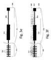
- FIGS. 3 a to 3 g are cross-sectional views illustrating a method of protecting alignment marks in accordance with an example of the present invention.
- FIGS. 3 a to 3 g are cross-sectional views illustrating a method of protecting alignment marks in accordance with an example of the present invention.
- a substrate 300 either p-type or n-type, may be provided.
- the substrate 300 may include a first area 310 on which device features are to be formed and one or more second area 311 provided with alignment mark trenches 307 .
- the first area 310 and the one or more second area 311 may be spaced apart from each other.
- the alignment mark trenches 307 may be formed by a patterning and etching process or other suitable process and each of the trenches 307 may have a depth of approximately 1200 angstrom ( ⁇ ), given a 75-nm (nanometer) flash memory process.
- a first dielectric layer 301 may then be formed on the substrate 300 by, for example, a thermal oxidation process.
- the first dielectric layer 301 may include silicon oxide such as silicon dioxide (SiO 2 ) or silicon oxynitride (SiON).
- the thickness of the first dielectric layer 301 may range from approximately 50 to 150 ⁇ , given the 75-nm process.
- a second dielectric layer 302 may be formed on the first dielectric layer 301 by a deposition process.
- the second dielectric layer 302 may include silicon nitride (Si 3 N 4 ) and have a thickness ranging from approximately 1400 to 1800 ⁇ .
- a patterned second dielectric layer 312 may be formed.
- the patterned second dielectric layer 312 may include a patterned region 308 at the first area 310 , exposing portions 320 of the substrate 300 .
- the second dielectric layer 302 over the alignment mark trenches 307 may be removed during the etching process, exposing the first dielectric layer 301 associated with the alignment mark trenches 307 .
- An opening 309 may thus be defined by the patterned second dielectric layer 312 and each of the alignment mark trenches 307 at the second area 311 .
- the substrate 300 may be etched through the exposed portions 320 so as to facilitate the formation of shallow trench isolation (STI) features.
- STI shallow trench isolation
- a third dielectric layer 330 may be formed on the patterned second dielectric layer 312 , resulting in STI features 321 at the first area 310 .
- the third dielectric layer 330 may include silicon oxide or silicon oxynitride and may have a thickness ranging from approximately 3000 to 4000 ⁇ .
- the third dielectric layer 330 except third dielectric 332 in the openings 309 may be removed by a first planarization process such as a chemical mechanical polishing (CMP) process, using the patterned second dielectric layer 312 as a stop layer.
- CMP chemical mechanical polishing
- the patterned second dielectric layer 312 in FIG. 3 d may be removed.
- the residual third dielectric 332 may consequently serve as alignment marks.
- a conductive layer 340 such as a polysilicon layer may be formed on the first dielectric layer 301 , the STI features 321 and the residual third dielectric 332 by, for example, a deposition process.
- the conductive layer 340 may have a thickness ranging from approximately 3000 to 4000 ⁇ .
- a patterned conductive layer 342 may be formed by a second planarization process such as a CMP process, using at least one of the STI features 321 or the residual third dielectric 332 as a stop layer.
- the residual third dielectric 332 , the STI features 321 and the patterned conductive layer 342 may be flush with one another over the substrate 300 after the second planarization process.
- the residual third dielectric 332 may include a first portion 3321 in the substrate 300 and a second portion 3322 over the substrate 300 .
- the specification may have presented the method and/or process of the present invention as a particular sequence of steps. However, to the extent that the method or process does not rely on the particular order of steps set forth herein, the method or process should not be limited to the particular sequence of steps described. As one of ordinary skill in the art would appreciate, other sequences of steps may be possible. Therefore, the particular order of the steps set forth in the specification should not be construed as limitations on the claims. In addition, the claims directed to the method and/or process of the present invention should not be limited to the performance of their steps in the order written, and one skilled in the art can readily appreciate that the sequences may be varied and still remain within the spirit and scope of the present invention.
Landscapes
- Element Separation (AREA)
Abstract
Description
Claims (4)
Priority Applications (1)
| Application Number | Priority Date | Filing Date | Title |
|---|---|---|---|
| US12/814,228 US8324743B2 (en) | 2010-06-11 | 2010-06-11 | Semiconductor device with a structure to protect alignment marks from damage in a planarization process |
Applications Claiming Priority (1)
| Application Number | Priority Date | Filing Date | Title |
|---|---|---|---|
| US12/814,228 US8324743B2 (en) | 2010-06-11 | 2010-06-11 | Semiconductor device with a structure to protect alignment marks from damage in a planarization process |
Publications (2)
| Publication Number | Publication Date |
|---|---|
| US20110304006A1 US20110304006A1 (en) | 2011-12-15 |
| US8324743B2 true US8324743B2 (en) | 2012-12-04 |
Family
ID=45095556
Family Applications (1)
| Application Number | Title | Priority Date | Filing Date |
|---|---|---|---|
| US12/814,228 Expired - Fee Related US8324743B2 (en) | 2010-06-11 | 2010-06-11 | Semiconductor device with a structure to protect alignment marks from damage in a planarization process |
Country Status (1)
| Country | Link |
|---|---|
| US (1) | US8324743B2 (en) |
Cited By (2)
| Publication number | Priority date | Publication date | Assignee | Title |
|---|---|---|---|---|
| US20150357287A1 (en) * | 2014-06-06 | 2015-12-10 | Taiwan Semiconductor Manufacturing Co., Ltd | Method for semiconductor wafer alignment |
| US10504960B2 (en) | 2017-09-12 | 2019-12-10 | Samsung Electronics Co., Ltd. | Semiconductor memory devices |
Citations (6)
| Publication number | Priority date | Publication date | Assignee | Title |
|---|---|---|---|---|
| US5783490A (en) | 1997-04-21 | 1998-07-21 | Vanguard International Semiconductor Corporation | Photolithography alignment mark and manufacturing method |
| US6218262B1 (en) * | 1997-09-09 | 2001-04-17 | Mitsubishi Denki Kabushiki Kaisha | Semiconductor device and method of manufacturing the same |
| US20020005594A1 (en) * | 1997-08-25 | 2002-01-17 | Mitsubishi Denki Kabushiki Kaisha | Semiconductor device and method for manufacturing the same |
| US20040198017A1 (en) * | 2003-01-28 | 2004-10-07 | Taiwan Semiconductor Manufacturing Company | Method to solve alignment mark blinded issues and technology for application of semiconductor etching at a tiny area |
| US20050101107A1 (en) * | 2003-11-12 | 2005-05-12 | Renesas Technology Corp. | Method for manufacturing semiconductor device |
| CN101452912A (en) | 2007-12-06 | 2009-06-10 | 台湾积体电路制造股份有限公司 | Apparatus and method for forming alignment marks on a backside surface |
-
2010
- 2010-06-11 US US12/814,228 patent/US8324743B2/en not_active Expired - Fee Related
Patent Citations (7)
| Publication number | Priority date | Publication date | Assignee | Title |
|---|---|---|---|---|
| US5783490A (en) | 1997-04-21 | 1998-07-21 | Vanguard International Semiconductor Corporation | Photolithography alignment mark and manufacturing method |
| US20020005594A1 (en) * | 1997-08-25 | 2002-01-17 | Mitsubishi Denki Kabushiki Kaisha | Semiconductor device and method for manufacturing the same |
| US6218262B1 (en) * | 1997-09-09 | 2001-04-17 | Mitsubishi Denki Kabushiki Kaisha | Semiconductor device and method of manufacturing the same |
| US20040198017A1 (en) * | 2003-01-28 | 2004-10-07 | Taiwan Semiconductor Manufacturing Company | Method to solve alignment mark blinded issues and technology for application of semiconductor etching at a tiny area |
| US20050101107A1 (en) * | 2003-11-12 | 2005-05-12 | Renesas Technology Corp. | Method for manufacturing semiconductor device |
| CN101452912A (en) | 2007-12-06 | 2009-06-10 | 台湾积体电路制造股份有限公司 | Apparatus and method for forming alignment marks on a backside surface |
| US20090146325A1 (en) * | 2007-12-06 | 2009-06-11 | Taiwan Semiconductor Manufacturing Company, Ltd. | Alignment for backside illumination sensor |
Non-Patent Citations (1)
| Title |
|---|
| Office Action from Chinese Patent Application No. 201010198798.7 dated Jul. 20, 2012. |
Cited By (4)
| Publication number | Priority date | Publication date | Assignee | Title |
|---|---|---|---|---|
| US20150357287A1 (en) * | 2014-06-06 | 2015-12-10 | Taiwan Semiconductor Manufacturing Co., Ltd | Method for semiconductor wafer alignment |
| US9601436B2 (en) * | 2014-06-06 | 2017-03-21 | Taiwan Semiconductor Manufacturing Co., Ltd | Method for semiconductor wafer alignment |
| US9952520B2 (en) | 2014-06-06 | 2018-04-24 | Taiwan Semiconductor Manufacturing Co., Ltd | Method for semiconductor wafer alignment |
| US10504960B2 (en) | 2017-09-12 | 2019-12-10 | Samsung Electronics Co., Ltd. | Semiconductor memory devices |
Also Published As
| Publication number | Publication date |
|---|---|
| US20110304006A1 (en) | 2011-12-15 |
Similar Documents
| Publication | Publication Date | Title |
|---|---|---|
| US5972793A (en) | Photolithography alignment mark manufacturing process in tungsten CMP metallization | |
| US6049137A (en) | Readable alignment mark structure formed using enhanced chemical mechanical polishing | |
| US6803291B1 (en) | Method to preserve alignment mark optical integrity | |
| US7709275B2 (en) | Method of forming a pattern for a semiconductor device and method of forming the related MOS transistor | |
| CN100407383C (en) | Method for polishing integrated circuit devices using dummy components | |
| US5923996A (en) | Method to protect alignment mark in CMP process | |
| JP4598047B2 (en) | Manufacturing method of semiconductor device | |
| US6465897B1 (en) | Method for photo alignment after CMP planarization | |
| CN102280367B (en) | Method for protecting alignment marks and semiconductor element formed by the method | |
| US9236240B2 (en) | Wafer edge protection | |
| US6624039B1 (en) | Alignment mark having a protective oxide layer for use with shallow trench isolation | |
| US8324743B2 (en) | Semiconductor device with a structure to protect alignment marks from damage in a planarization process | |
| US7307002B2 (en) | Non-critical complementary masking method for poly-1 definition in flash memory device fabrication | |
| US7332419B2 (en) | Structure and method of fabricating a transistor having a trench gate | |
| US20060148275A1 (en) | Method of forming an alignment mark and manufacturing a semiconductor device using the same | |
| US6979651B1 (en) | Method for forming alignment features and back-side contacts with fewer lithography and etch steps | |
| KR20010003670A (en) | Method for forming alignment key of semiconductor device | |
| US7968418B1 (en) | Apparatus and method for isolating integrated circuit components using deep trench isolation and shallow trench isolation | |
| US6958280B2 (en) | Method for manufacturing alignment mark of semiconductor device using STI process | |
| TWI416613B (en) | Method for protecting alignment mark and semiconductor element formed by the same | |
| US7452818B2 (en) | Method for selectively etching portions of a layer of material based upon a density or size of semiconductor features located thereunder | |
| JP3589580B2 (en) | Method for manufacturing semiconductor device | |
| KR100835420B1 (en) | Manufacturing Method of Semiconductor Device | |
| CN120630596A (en) | Overlay error control method | |
| TW200410339A (en) | Mask with extended mask clear-out window and method of dummy exposure using the same |
Legal Events
| Date | Code | Title | Description |
|---|---|---|---|
| AS | Assignment |
Owner name: MACRONIX INTERNATIONAL CO., LTD., CHINA Free format text: ASSIGNMENT OF ASSIGNORS INTEREST;ASSIGNORS:YEH, CHIAO-WEN;HUANG, CHIH-HAO;REEL/FRAME:024525/0709 Effective date: 20100528 |
|
| ZAAA | Notice of allowance and fees due |
Free format text: ORIGINAL CODE: NOA |
|
| ZAAB | Notice of allowance mailed |
Free format text: ORIGINAL CODE: MN/=. |
|
| ZAAA | Notice of allowance and fees due |
Free format text: ORIGINAL CODE: NOA |
|
| STCF | Information on status: patent grant |
Free format text: PATENTED CASE |
|
| CC | Certificate of correction | ||
| FPAY | Fee payment |
Year of fee payment: 4 |
|
| MAFP | Maintenance fee payment |
Free format text: PAYMENT OF MAINTENANCE FEE, 8TH YEAR, LARGE ENTITY (ORIGINAL EVENT CODE: M1552); ENTITY STATUS OF PATENT OWNER: LARGE ENTITY Year of fee payment: 8 |
|
| FEPP | Fee payment procedure |
Free format text: MAINTENANCE FEE REMINDER MAILED (ORIGINAL EVENT CODE: REM.); ENTITY STATUS OF PATENT OWNER: LARGE ENTITY |
|
| LAPS | Lapse for failure to pay maintenance fees |
Free format text: PATENT EXPIRED FOR FAILURE TO PAY MAINTENANCE FEES (ORIGINAL EVENT CODE: EXP.); ENTITY STATUS OF PATENT OWNER: LARGE ENTITY |
|
| STCH | Information on status: patent discontinuation |
Free format text: PATENT EXPIRED DUE TO NONPAYMENT OF MAINTENANCE FEES UNDER 37 CFR 1.362 |
|
| FP | Lapsed due to failure to pay maintenance fee |
Effective date: 20241204 |