US8310300B2 - Charge pump having ramp rate control - Google Patents
Charge pump having ramp rate control Download PDFInfo
- Publication number
- US8310300B2 US8310300B2 US12/870,464 US87046410A US8310300B2 US 8310300 B2 US8310300 B2 US 8310300B2 US 87046410 A US87046410 A US 87046410A US 8310300 B2 US8310300 B2 US 8310300B2
- Authority
- US
- United States
- Prior art keywords
- output
- input
- coupled
- register
- counter
- Prior art date
- Legal status (The legal status is an assumption and is not a legal conclusion. Google has not performed a legal analysis and makes no representation as to the accuracy of the status listed.)
- Active, expires
Links
- 230000004044 response Effects 0.000 claims abstract description 38
- 239000003990 capacitor Substances 0.000 claims abstract description 33
- 230000000630 rising effect Effects 0.000 claims description 6
- 230000008878 coupling Effects 0.000 claims description 4
- 238000010168 coupling process Methods 0.000 claims description 4
- 238000005859 coupling reaction Methods 0.000 claims description 4
- 230000008859 change Effects 0.000 description 34
- 230000033228 biological regulation Effects 0.000 description 16
- 238000000034 method Methods 0.000 description 12
- 230000008569 process Effects 0.000 description 12
- 238000012512 characterization method Methods 0.000 description 10
- 239000013256 coordination polymer Substances 0.000 description 6
- 230000007704 transition Effects 0.000 description 6
- 238000010586 diagram Methods 0.000 description 5
- 230000003247 decreasing effect Effects 0.000 description 4
- 230000007423 decrease Effects 0.000 description 3
- 238000009499 grossing Methods 0.000 description 3
- 230000008901 benefit Effects 0.000 description 2
- 230000004048 modification Effects 0.000 description 2
- 238000012986 modification Methods 0.000 description 2
- 238000005086 pumping Methods 0.000 description 2
- 238000004088 simulation Methods 0.000 description 2
- 230000000694 effects Effects 0.000 description 1
- 238000005516 engineering process Methods 0.000 description 1
- 230000015654 memory Effects 0.000 description 1
- 238000012913 prioritisation Methods 0.000 description 1
- 230000001105 regulatory effect Effects 0.000 description 1
- 230000002123 temporal effect Effects 0.000 description 1
Images


Classifications
-
- H—ELECTRICITY
- H02—GENERATION; CONVERSION OR DISTRIBUTION OF ELECTRIC POWER
- H02M—APPARATUS FOR CONVERSION BETWEEN AC AND AC, BETWEEN AC AND DC, OR BETWEEN DC AND DC, AND FOR USE WITH MAINS OR SIMILAR POWER SUPPLY SYSTEMS; CONVERSION OF DC OR AC INPUT POWER INTO SURGE OUTPUT POWER; CONTROL OR REGULATION THEREOF
- H02M3/00—Conversion of dc power input into dc power output
- H02M3/02—Conversion of dc power input into dc power output without intermediate conversion into ac
- H02M3/04—Conversion of dc power input into dc power output without intermediate conversion into ac by static converters
- H02M3/06—Conversion of dc power input into dc power output without intermediate conversion into ac by static converters using resistors or capacitors, e.g. potential divider
- H02M3/07—Conversion of dc power input into dc power output without intermediate conversion into ac by static converters using resistors or capacitors, e.g. potential divider using capacitors charged and discharged alternately by semiconductor devices with control electrode, e.g. charge pumps
Definitions
- This disclosure relates generally to charge pumps, and more specifically, to charge pumps having ramp rate control.
- NVMs non-volatile memories
- Some NVM technologies require a charge pump voltage with a controlled ramp rate.
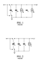
- the ramp rate is either controlled by a shunt current Ish that consumes some of the charge produced by the pump as shown in FIG. 1 .
- the size of the charging capacitor is adjusted to modulate the amount of charge produced by the pump as shown in FIG. 2 .
- the ramp rate is proportional to the size of a smoothing capacitor (Csm) and a load capacitor Cl, and the magnitude of the load Ild and shunt currents Ish.
- the ramp rate is inversely proportional to the charging capacitor (Cp) and the clock frequency.
- Selecting a shunt current or a charging capacitor size can be complicated by the variability of the load capacitance and current and overall power consumption. Those values will depend on the number of bits that are programmed; precise control of the ramp rate for all operating conditions using prior art is therefore impossible. The situation can be mitigated somewhat by selecting a large smoothing capacitor that swamps the effect of changing load capacitance and current at the expense of die area and increased power consumption during ramping. Without the increase in smoothing capacitor an increase in load can dramatically slow the ramp rate as illustrated in the simulation shown in FIG. 3 that compares two loads, one of which is 2.5 times the other. For the simulation shown in FIG. 3 the pump consisted of a single stage with 3V input and 5V regulation point.
- FIG. 1 is a circuit diagram of a charge pump of the prior art of a first type
- FIG. 2 is a circuit diagram of a charge pump of the prior art of a second type
- FIG. 3 is a graph showing a charge pump characteristic of the prior art
- FIG. 4 is a circuit diagram of a charge pump that controls a ramp-up of the output voltage
- FIG. 5 is a circuit diagram of a charge pump of FIG. 4 with additional features
- FIG. 6 is a diagram of a plurality of signals present in the charge pump of FIG. 5 ;
- FIG. 7 a graph showing a charge pump characteristic of the prior art and the charge pump of FIG. 5 .
- a charge pump has a counter that provides an output to a digital to analog (D/A) converter which in turn provides an analog signal to a comparator.
- the comparator compares the output of the D/A converter to the output of the charge pump to determine if the output is following the desired ramp rate. If a faster ramp rate is desired, more capacitance is added to the pumping process. If the ramp rate exceeds the desired ramp rate, capacitance is subtracted from the pumping process.
- FIG. 4 shows a charge pump that can control its ramp rate independently from its load. During each clock cycle it compares the pump output value to the desired output value for that cycle and adjusts the value of the charging capacitor to increase or decrease the ramp rate.
- FIG. 4 shows a charge pump 10 comprising an UP counter 12 , a D/A converter 14 having an input coupled to the output of UP counter 12 , a comparator 16 having a first input coupled to the output of D/A converter 14 , an up/down (U/D) counter 18 having an input coupled to the output of comparator 16 , a variable capacitor charge pump 20 having an input coupled to the output of U/D counter 18 , and a load 22 coupled to an output of variable capacitor charge pump 20 .
- the output of variable capacitor charge pump 20 is the output of charge pump 10 and is coupled to a second input of comparator 16 .
- Variable capacitor charge pump 20 may be referenced as pump stage having a variable capacitor.
- the output value of UP counter 12 which increases with each clock, is converted to an analog voltage value by D/A converter 14 and the voltage value is applied to the first input of comparator 16 .
- the output value of a counter may be referenced a count value. Since the second input of comparator 16 is connected to the output of pump 20 , the output of comparator 16 will be the sign of the difference between the output value of D/A converter 14 and the output value, Vout, of pump 20 . If the output value of pump 20 , Vout, is greater than the output value of D/A converter 14 , the amount of charging capacitance of pump 20 is reduced and the incremental increase in the change of the pump 20 output value, Vout, is decreased during the succeeding clock period.
- the amount of the charging capacitance of pump 20 is increased and the incremental increase in the change of the pump 20 output value, Vout, is increased during the succeeding clock period.
- the ramp rate for the output voltage of pump 10 , Vout will be determined by the LSB size of the D/A converter 14 and the Up counter 12 clock frequency.
- FIG. 5 shows a charge pump 30 with circuitry added to charge pump 10 of FIG. 4 and also shows UP counter 12 and U/D counter 18 in more detail.
- the input of comparator 16 can be multiplexed between the ramp rate control voltage value and the regulation voltage value by adding register 32 and switch 44 to the input of D/A converter 14 and two D flip-flops (DFFs), 34 and 36 , to the output of comparator 16 .
- DFFs D flip-flops
- charge pump 30 includes clock logic 38 , logic 42 , and RS flip flop (RSFF) 40 .
- Up-counter 12 includes register 45 , adder 46 , and register 48 .
- U/D counter 18 includes register 50 , adder/subtractor 52 , and register 54 .
- Switch 44 has a first terminal coupled to the input of D/A converter 14 , a second terminal coupled to the output of register 32 , and a third terminal coupled to the output of up-counter 12 , which is the output of register 48 . The position of the switch is controlled by the state of clock C 4 .
- Adder 46 has a first input coupled to the output of register 48 , a second input coupled to the output of register 45 , and an output coupled to an input of register 48 .
- the loading of register 48 is controlled by the state of clock C 4 .
- Adder/subtractor 52 has a first input coupled to the output of register 54 , which is also the output of U/D counter 18 , a second input coupled to the output of register 50 , a control input coupled to an output of DFF 34 , and an output coupled to an input of register 54 .
- the loading of register 54 is controlled by the state of clock C 4 .
- Registers 50 and 45 contain interval values for incrementing and decrementing U/D counter 18 and incrementing up-counter 12 .
- DFF 34 has a data input coupled to the output of comparator 16 , a clock input for receiving clock C 1 , and an output connected to the control input of adder/subtractor 52 .
- DFF 36 has a clock input for receiving clock C 2 , a data input coupled to the output of comparator 16 , and an output coupled to an input of logic 42 and the set input, S, of RSFF 40 .
- Logic 42 has an input connected to the output of DFF 36 , an input connected to clock C 3 , and an output that provides a pump clock CP.
- Charge pump 20 has an input coupled to the output of logic 42 (CP in FIG. 5 ), an input coupled to the output of U/D counter 18 and an output coupled to the second input of comparator 16 as well as load 22 .
- RSFF 40 has a set input, S, coupled to the output of DFF 36 , a reset input, R, coupled to RESET, and an output, Rsout, coupled to a control input of clock logic 38 .
- Clock logic 38 has an input connected to the output of RSFF, Rsout, and an input connected to the main clock, CLK.
- Clock logic 38 provides clocks C 1 , C 2 , C 3 , and C 4 in response to master clock CLK. The relationship of these clocks is shown in FIG. 6 .
- Register 32 contains the D/A input value for regulation (Vreg in FIG. 6 ). Regulation occurs when the output of pump 20 is controlled to a value close to the value of the desired pump output voltage, such as the voltage value required for programming or erasing NVM. As illustrated in FIG. 6 , during the ramping process that precedes regulation the output value of D/A converter 14 , DAout, alternates between the regulation value and the ramp control value. During the regulation process (not shown in FIG. 6 ) the output value of D/A converter 14 , DAout, is equal to the regulation voltage value, Vreg.
- DFF 34 will store the comparator output state in response to a positive edge of clock C 1 ; because of its connection to u/d-counter 18 the output state of DFF 34 will ultimately determine the capacitance value in the variable capacitance charge pump 20 .
- DFF 36 will store the comparator output state in response to a positive edge of clock C 2 in FIG. 6 ; because of its connection to logic 42 the output state of DFF 36 will determine the active condition of the variable capacitance charge pump 20 .
- register 45 is loaded with an interval value that will determine the amount that the output value of counter 12 is increased during each cycle. Taking the example that register 45 is loaded with “2” and register 48 is loaded with “0”, adder 46 provides an output of “2”.
- a positive transition of clock C 4 causes Register 48 to change its output to “2” and since the output of register 48 is coupled to an input of adder 46 , adder 46 provides an output of “4” in response to the change in the output of register 48 .
- register 48 changes its output to “4” to match the input provided by adder 46 , which in turn causes adder 46 to change its output to “6”. The process continues with each positive edge of clock C 4 , sequentially increasing the value presented to switch 44 by “2”.
- Register 50 is loaded with an interval value that will determine the incremental amount of capacitance that will be added to or subtracted from the total capacitance in the variable capacitance charge pump 20 . Taking the example that register 50 is loaded with “2” and register 54 is loaded with “8,” the output value of the adder/subtractor 52 will be “10” if the output of DFF 34 is logic level high and “6” if the output of DFF 34 is logic level low.
- a positive transition of clock C 4 causes register 54 to change its output such that it is the same value as the output value of the adder/subtractor 52 .
- the adder/subtractor 52 will change its output to “12” or “4” depending on the state of the output of DFF 34 .
- the variable capacitance charge pump 20 will add or subtract capacitance.
- the ramping process begins at time t 0 shown in FIG. 6 .
- Clock C 1 is active and aligned with master clock CLK while the other clocks, clocks C 2 , C 3 and C 4 , are at a logic low.
- Registers 45 and 50 have been loaded with interval values and register 32 has been loaded with the regulation value. Since clock C 4 is at a logic low, switch 44 couples the output of UP counter 12 to the input of D/A converter 14 .
- the output value of D/A converter 14 is equal to the first ramp step target voltage level for Vout.
- Comparator 16 compares the value of D/A converter 14 output, DAout, to the value of Vout; the resulting sign of the difference between the two values is loaded into DFF 34 on the positive edge of clock C 1 .
- the output of DFF 34 is connected to the control input of adder/subtractor 52 and determines whether adder/subtractor 52 is configured as an adder or a subtractor; therefore the output of adder/subtractor 52 is either the sum or the difference of the values contained in register 54 and register 50 .
- the output of adder/subtractor 52 is the difference of the two registers when the output of DFF 34 indicates that the value of Vout is greater than the value of DAout, a condition that occurs when the ramp rate is too fast and needs to be decreased.
- the output of adder/subtractor 52 is the sum of the two registers when the output of DFF 34 indicates that the value of Vout is less than the value of DAout, a condition that occurs when the ramp rate is too slow and needs to be increased. Because the output of adder/subtractor 52 is connected to an input of register 54 , the output state of register 54 changes to match the output of adder/subtractor 52 on the positive edge of clock C 4 (t 1 in FIG. 6 ); this change causes an appropriate change in the capacitance of pump 20 .
- clock C 4 switches state so that switch 44 connects the output of register 32 to the input of D/A converter 14 .
- the output value of D/A converter 14 , DAout is equal to the desired regulation voltage (shown as Vreg in FIG. 6 ).
- the output of D/A converter 14 , DAout is connected to the input of comparator 16 , which compares the value of Vreg to the value of Vout. Because the output of comparator 16 is connected to the input of DFF 36 , DFF 36 will store the output state of comparator 16 at the next positive edge of clock C 2 , (t 2 in FIG. 6 ).
- switch 44 again couples the output of register 32 to the input of D/A converter 14 .
- the output value of the D/A converter 14 , DAout will again equal the value of Vreg.
- Comparator 16 again compares the value of DAout and the value of Vout; if the value of Vout is still less than the value of Vreg there will be no change in the output of DFF 36 in response to the next positive edge of clock C 2 (t 6 in FIG. 6 ) and thus no change in RSFF or logic 42 . Since logic 42 does not inhibit clock C 3 the output value of pump 20 , Vout, continues to increase in responses to changes in CP. At the next negative edge of C 4 (t 7 in FIG.
- switch 44 connects the output of counter 12 , which has been increased by the interval value contained in register 45 , to the input of D/A converter 14 .
- the output value of D/A converter 14 equals the next desired ramp value for the time in the ramp process. Since the output of D/A converter 14 is connected to the input of comparator 16 , the output state of comparator 16 will change to equal the sign of the difference between DAout and Vout. DFF 34 will store this state at the next positive edge of C 1 (t 8 in FIG. 6 ).
- logic 42 In response to the change in the output state of DFF 36 logic 42 will cease to inhibit clock C 3 and the resulting changes in the value of CP in response to changes in clock C 3 will cause the output value of pump 20 , Vout, to increase until the value of Vout again exceeds the value of Vreg.
- This process of regulating Vout to a value greater than or equal to the value of Vreg will continue as long as Vout is needed, as for example programming or erasing NVM.
- the output state of RSFF 40 , Rsout will not respond to any additional changes in the output state of FF 36 , however. Rsout will not change again until the reset signal RESET causes the output of RSFF 40 , Rsout, to change state. This operation continues as shown in FIG. 6 for times t 9 , t 10 , t 11 , t 12 , and t 13 .
- FIG. 7 illustrates the operation of the charge pump of the prior art and the operation of the invention under a variety of loads.
- the left-most trace labeled “No Control, 1 ⁇ Load” is the operation of the charge pump of the prior art with a minimal load. The output value of the pump reaches the regulation value in approximately 2 us.
- the right-most trace labeled “No Control, 2.5 ⁇ Load”, is the operation of the charge pump of the prior art when the load is increased to two and a half times the minimal load. The output value of the pump reaches the regulation value in approximately 4 us. The difference in ramp rate between the minimal load case and the larger load case is unacceptable for certain applications.
- a charge pump having a first counter and a pump stage.
- the first counter has a control input for receiving a control signal, and an output for providing a first count value, wherein the first count value is incremented in response to the control signal being a first logic state and the first count value is decremented in response to the control signal being a second logic state.
- the pump stage has a variable capacitor, the variable capacitor having a control input coupled to the output of the first counter for receiving the first count value, wherein a capacitance value of the variable capacitor is changed in response to the first count value changing, and wherein the capacitance value is for determining a ramp-up rate of an output voltage at an output of the charge pump.
- the charge pump may further include a second counter having an output for providing a second count value, a digital-to-analog converter having an input coupled to the output of the second counter, and an output for providing an analog representation of the second count value, and a comparator having a first input coupled to the output of the digital-to-analog converter, a second input coupled to the output of the charge pump, and an output for providing the control signal to the control input of the first counter.
- the charge pump may further include a switch coupled between the output of the second counter and the input of the digital-to-analog converter, the switch having a control input for receiving a first clock signal.
- the charge pump may further include a register for storing a digital value corresponding to a desired output voltage at the output of the charge pump, the register having an output selectively coupled to the input of the digital-to-analog converter, wherein the switch alternately couples the second count value and the digital value to the input of the digital-to-analog converter in response to the first clock signal.
- the charge pump may further include a first flip-flop having an input coupled to the output of the comparator, an output coupled to the control input of the variable capacitor, and a clock input for receiving a second clock signal and a second flip-flop having an input coupled to the output of the comparator, an output coupled to the pump stage, and a clock input for receiving a third clock signal.
- the charge pump may have a further characterization by which the second clock signal and the third clock signal are characterized as being non-overlapping clock signals.
- the charge pump may have a further characterization by which the first flip-flop responds to rising edges of the second clock signal and second flip-flop responds to rising edges of the third clock signal.
- the charge pump may have a further characterization by which the first counter includes a first register for storing an interval value, the first register having an output, an adder having a first input coupled to the output of the first register, a second input, a control input, and an output, and a second register having in input coupled to the output of the adder, and an output coupled to the second input of the adder.
- the charge pump may have a further characterization by which the charge pump is implemented on a single integrated circuit.
- a charge pump including a first counter having an output for providing a first count value.
- the charge pump further includes a digital-to-analog converter having an input coupled to the output of the first counter, and an output for providing an analog representation of the first count value.
- the charge pump further includes a comparator having a first input coupled to the output of the digital-to-analog converter, a second input, and an output.
- the charge pump further includes a second counter having an input coupled to the output of the comparator, and an output for providing a second count value.
- the charge pump further includes a pump stage having an input, an output coupled to the second input of the comparator, and a variable capacitor, a capacitance value of the variable capacitor being changed in response to the second count value.
- the charge pump may have a further characterization by which the first counter comprises a first register having an output, an adder having a first input coupled to the output of the first register, a second input, and an output, and a second register having an input coupled to the output of the adder, and an output coupled to the second input of the adder.
- the charge pump may have a further characterization by which the second counter comprises a third register having an output, an adder/subtractor having a first input coupled to the output of the third register, a second input, and an output, and a fourth register having an input coupled to the output of the adder/subtractor, and an output coupled to the second input of the adder/subtractor.
- the charge pump may further include a fifth register for storing a digital value corresponding to a desired output voltage at the output of the pump stage, wherein the digital value and the first count value are alternately provided to the input of the digital-to-analog converter.
- the charge pump may further include a switch, the switch for alternately coupling the output of the second register and an output of the fifth register to the input of the digital-to-analog converter in response to a clock signal.
- the charge pump may further include a first logic circuit coupled between the output of the comparator and the input of the second counter.
- the charge pump may have a further characterization by which the charge pump is implemented in a single integrated circuit.
- a charge pump including a first counter having an output for providing a first count value.
- the charge pump further includes a digital-to-analog converter having an input and an output.
- the charge pump further includes a first register for storing a digital value corresponding to a desired output voltage at an output of the charge pump.
- the charge pump further includes a switch having a first terminal coupled to the output of the first register, a second terminal coupled to the output of the first counter, and a third terminal coupled to the input of the digital-to-analog converter, wherein the digital value and the first count value are alternately provided to the input of the digital-to-analog converter in response to a clock signal.
- the charge pump further includes a comparator having a first input coupled to the output of the digital-to-analog converter, a second input, and an output.
- the charge pump further includes a second counter having an input coupled to the output of the comparator, and an output for providing a second count value.
- the charge pump further includes a pump stage having a variable capacitor, the variable capacitor having an input coupled to the output of the second counter for receiving the second count value, the pump stage having an output coupled to the second input of the comparator, the pump stage having a clock input coupled to the output of the comparator.
- the charge pump may have a further characterization by which the second counter is an up/down counter, wherein the up/down counter increments the second count value in response to the output of the comparator being a first logic state, and the up/down counter decrements the second count value in response to the output of the comparator being a second logic state.
- the charge pump may have a further characterization by which the first counter includes a first register having an output, an adder having a first input coupled to the output of the first register, a second input, and an output, and a second register having an input coupled to the output of the adder, and an output coupled to the second input of the adder.
- the charge pump may have a further characterization by which the second counter comprises a first register having an output, an adder/subtractor having a first input coupled to the output of the first register, a second input, and an output, and a second register having an input coupled to the output of the adder/subtractor, and an output coupled to the second input of the adder/subtractor.
- Coupled is not intended to be limited to a direct coupling or a mechanical coupling.
Abstract
Description
Claims (15)
Priority Applications (4)
| Application Number | Priority Date | Filing Date | Title |
|---|---|---|---|
| US12/870,464 US8310300B2 (en) | 2010-08-27 | 2010-08-27 | Charge pump having ramp rate control |
| EP11176623.4A EP2424094B1 (en) | 2010-08-27 | 2011-08-04 | Charge pump having ramp rate control |
| TW100128354A TWI521844B (en) | 2010-08-27 | 2011-08-09 | Charge pump having ramp rate control |
| CN201110248478.2A CN102386763B (en) | 2010-08-27 | 2011-08-26 | There is the electric charge pump that ramp rate controls |
Applications Claiming Priority (1)
| Application Number | Priority Date | Filing Date | Title |
|---|---|---|---|
| US12/870,464 US8310300B2 (en) | 2010-08-27 | 2010-08-27 | Charge pump having ramp rate control |
Publications (2)
| Publication Number | Publication Date |
|---|---|
| US20120049917A1 US20120049917A1 (en) | 2012-03-01 |
| US8310300B2 true US8310300B2 (en) | 2012-11-13 |
Family
ID=44582340
Family Applications (1)
| Application Number | Title | Priority Date | Filing Date |
|---|---|---|---|
| US12/870,464 Active 2030-12-23 US8310300B2 (en) | 2010-08-27 | 2010-08-27 | Charge pump having ramp rate control |
Country Status (4)
| Country | Link |
|---|---|
| US (1) | US8310300B2 (en) |
| EP (1) | EP2424094B1 (en) |
| CN (1) | CN102386763B (en) |
| TW (1) | TWI521844B (en) |
Cited By (3)
| Publication number | Priority date | Publication date | Assignee | Title |
|---|---|---|---|---|
| US20170092357A1 (en) * | 2015-09-24 | 2017-03-30 | Stmicroelectronics (Rousset) Sas | Method for Managing the Write Cycle of an EEPROM |
| US9653990B1 (en) * | 2015-11-20 | 2017-05-16 | STMicroelectronics (Shenzhen) R&D Co. Ltd | Negative charge pump with soft start |
| US11881280B2 (en) | 2020-11-30 | 2024-01-23 | Stmicroelectronics International N.V. | Circuit and method for constant slew rate in high voltage charge pumps |
Families Citing this family (13)
| Publication number | Priority date | Publication date | Assignee | Title |
|---|---|---|---|---|
| US9124296B2 (en) | 2012-06-27 | 2015-09-01 | Analog Devices Global | Multi-stage string DAC |
| US8912940B2 (en) * | 2012-11-14 | 2014-12-16 | Analog Devices Technology | String DAC charge boost system and method |
| US8912939B2 (en) | 2012-12-14 | 2014-12-16 | Analog Devices Technology | String DAC leakage current cancellation |
| US9553567B2 (en) * | 2013-06-03 | 2017-01-24 | Qorvo Us, Inc. | Fast settling charge pump with frequency hopping |
| TWI523389B (en) * | 2013-08-16 | 2016-02-21 | Sitronix Technology Corp | A power supply circuit with a complex charge pump |
| TWI512714B (en) * | 2013-08-19 | 2015-12-11 | Sitronix Technology Corp | A power supply circuit of a display device |
| US9088280B2 (en) | 2013-10-30 | 2015-07-21 | Freescale Semiconductor, Inc. | Body bias control circuit |
| EP2884643B1 (en) * | 2013-12-11 | 2022-07-13 | Nxp B.V. | DC-DC voltage converter and conversion method |
| US9653126B2 (en) * | 2014-01-27 | 2017-05-16 | Sandisk Technologies Llc | Digital ramp rate control for charge pumps |
| US11515067B2 (en) | 2018-02-22 | 2022-11-29 | Aalborg Universitet | Two-terminal active inductor device |
| CN111771323A (en) | 2018-02-22 | 2020-10-13 | 奥尔堡大学 | Two-terminal active capacitor device |
| US10804794B2 (en) * | 2018-09-19 | 2020-10-13 | Dialog Semiconductor (Uk) Limited | System and method for controlling a charge pump |
| CN109639134A (en) * | 2019-01-11 | 2019-04-16 | 上海艾为电子技术股份有限公司 | A kind of slope control circuit |
Citations (17)
| Publication number | Priority date | Publication date | Assignee | Title |
|---|---|---|---|---|
| US4326134A (en) | 1979-08-31 | 1982-04-20 | Xicor, Inc. | Integrated rise-time regulated voltage generator systems |
| US5168174A (en) | 1991-07-12 | 1992-12-01 | Texas Instruments Incorporated | Negative-voltage charge pump with feedback control |
| US5222111A (en) * | 1990-10-29 | 1993-06-22 | Mitsubishi Denki Kabushiki Kaisha | Pulse generator circuit employing arithmetic function counter |
| US5365121A (en) | 1993-03-08 | 1994-11-15 | Motorola Inc. | Charge pump with controlled ramp rate |
| US5563779A (en) * | 1994-12-05 | 1996-10-08 | Motorola, Inc. | Method and apparatus for a regulated supply on an integrated circuit |
| US5801987A (en) | 1997-03-17 | 1998-09-01 | Motorola, Inc. | Automatic transition charge pump for nonvolatile memories |
| US5945870A (en) | 1996-07-18 | 1999-08-31 | Altera Corporation | Voltage ramp rate control circuit |
| US6320796B1 (en) * | 2000-11-10 | 2001-11-20 | Marvell International, Ltd. | Variable slope charge pump control |
| US6693410B1 (en) | 2002-12-16 | 2004-02-17 | Adc Dsl Systems, Inc. | Power sequencing and ramp rate control circuit |
| US6724241B1 (en) | 2002-10-25 | 2004-04-20 | Atmel Corporation | Variable charge pump circuit with dynamic load |
| US20050057675A1 (en) * | 2003-09-17 | 2005-03-17 | Korea Advanced Institute Of Science And Technology | CMOS image sensor |
| US6980047B1 (en) | 2002-06-20 | 2005-12-27 | Taiwan Semiconductor Manufacturing Company | Low power high voltage ramp-up control circuit |
| US7123067B2 (en) * | 2002-05-28 | 2006-10-17 | Sony Corporation | Voltage-change control circuit and method |
| US20090097285A1 (en) | 2007-10-10 | 2009-04-16 | Cook Thomas D | Variable load, variable output charge-based voltage multipliers |
| US7542351B2 (en) | 2007-05-31 | 2009-06-02 | Freescale Semiconductor, Inc. | Integrated circuit featuring a non-volatile memory with charge/discharge ramp rate control and method therefor |
| US20090168586A1 (en) | 2005-11-30 | 2009-07-02 | Atmel Corporation | Circuit to control voltage ramp rate |
| US7630250B2 (en) | 2007-10-16 | 2009-12-08 | Spansion Llc | Controlled ramp rates for metal bitlines during write operations from high voltage driver for memory applications |
Family Cites Families (1)
| Publication number | Priority date | Publication date | Assignee | Title |
|---|---|---|---|---|
| US7173477B1 (en) * | 2003-12-19 | 2007-02-06 | Cypress Semiconductor Corp. | Variable capacitance charge pump system and method |
-
2010
- 2010-08-27 US US12/870,464 patent/US8310300B2/en active Active
-
2011
- 2011-08-04 EP EP11176623.4A patent/EP2424094B1/en active Active
- 2011-08-09 TW TW100128354A patent/TWI521844B/en active
- 2011-08-26 CN CN201110248478.2A patent/CN102386763B/en active Active
Patent Citations (17)
| Publication number | Priority date | Publication date | Assignee | Title |
|---|---|---|---|---|
| US4326134A (en) | 1979-08-31 | 1982-04-20 | Xicor, Inc. | Integrated rise-time regulated voltage generator systems |
| US5222111A (en) * | 1990-10-29 | 1993-06-22 | Mitsubishi Denki Kabushiki Kaisha | Pulse generator circuit employing arithmetic function counter |
| US5168174A (en) | 1991-07-12 | 1992-12-01 | Texas Instruments Incorporated | Negative-voltage charge pump with feedback control |
| US5365121A (en) | 1993-03-08 | 1994-11-15 | Motorola Inc. | Charge pump with controlled ramp rate |
| US5563779A (en) * | 1994-12-05 | 1996-10-08 | Motorola, Inc. | Method and apparatus for a regulated supply on an integrated circuit |
| US5945870A (en) | 1996-07-18 | 1999-08-31 | Altera Corporation | Voltage ramp rate control circuit |
| US5801987A (en) | 1997-03-17 | 1998-09-01 | Motorola, Inc. | Automatic transition charge pump for nonvolatile memories |
| US6320796B1 (en) * | 2000-11-10 | 2001-11-20 | Marvell International, Ltd. | Variable slope charge pump control |
| US7123067B2 (en) * | 2002-05-28 | 2006-10-17 | Sony Corporation | Voltage-change control circuit and method |
| US6980047B1 (en) | 2002-06-20 | 2005-12-27 | Taiwan Semiconductor Manufacturing Company | Low power high voltage ramp-up control circuit |
| US6724241B1 (en) | 2002-10-25 | 2004-04-20 | Atmel Corporation | Variable charge pump circuit with dynamic load |
| US6693410B1 (en) | 2002-12-16 | 2004-02-17 | Adc Dsl Systems, Inc. | Power sequencing and ramp rate control circuit |
| US20050057675A1 (en) * | 2003-09-17 | 2005-03-17 | Korea Advanced Institute Of Science And Technology | CMOS image sensor |
| US20090168586A1 (en) | 2005-11-30 | 2009-07-02 | Atmel Corporation | Circuit to control voltage ramp rate |
| US7542351B2 (en) | 2007-05-31 | 2009-06-02 | Freescale Semiconductor, Inc. | Integrated circuit featuring a non-volatile memory with charge/discharge ramp rate control and method therefor |
| US20090097285A1 (en) | 2007-10-10 | 2009-04-16 | Cook Thomas D | Variable load, variable output charge-based voltage multipliers |
| US7630250B2 (en) | 2007-10-16 | 2009-12-08 | Spansion Llc | Controlled ramp rates for metal bitlines during write operations from high voltage driver for memory applications |
Cited By (6)
| Publication number | Priority date | Publication date | Assignee | Title |
|---|---|---|---|---|
| US20170092357A1 (en) * | 2015-09-24 | 2017-03-30 | Stmicroelectronics (Rousset) Sas | Method for Managing the Write Cycle of an EEPROM |
| US10068644B2 (en) * | 2015-09-24 | 2018-09-04 | Stmicroelectronics (Rousset) Sas | System and method for adjusting EEPROM write cycle duration according to supply voltage variation |
| US10210933B2 (en) | 2015-09-24 | 2019-02-19 | Stmicroelectronics (Rousset) Sas | System and method for adjusting EEPROM write cycle duration according to supply voltage variation |
| US9653990B1 (en) * | 2015-11-20 | 2017-05-16 | STMicroelectronics (Shenzhen) R&D Co. Ltd | Negative charge pump with soft start |
| US20170149328A1 (en) * | 2015-11-20 | 2017-05-25 | STMicroelectronics (Shenzhen) R&D Co. Ltd | Negative charge pump with soft start |
| US11881280B2 (en) | 2020-11-30 | 2024-01-23 | Stmicroelectronics International N.V. | Circuit and method for constant slew rate in high voltage charge pumps |
Also Published As
| Publication number | Publication date |
|---|---|
| EP2424094B1 (en) | 2019-12-11 |
| TWI521844B (en) | 2016-02-11 |
| CN102386763A (en) | 2012-03-21 |
| TW201214939A (en) | 2012-04-01 |
| EP2424094A3 (en) | 2017-01-11 |
| EP2424094A2 (en) | 2012-02-29 |
| CN102386763B (en) | 2016-07-06 |
| US20120049917A1 (en) | 2012-03-01 |
Similar Documents
| Publication | Publication Date | Title |
|---|---|---|
| US8310300B2 (en) | Charge pump having ramp rate control | |
| US8912778B1 (en) | Switching voltage regulator employing current pre-adjust based on power mode | |
| US7276960B2 (en) | Voltage regulated charge pump with regulated charge current into the flying capacitor | |
| EP2725694B1 (en) | System and method for generating a regulated boosted voltage using a controlled variable number of charge pump circuits | |
| US7741899B2 (en) | Step-up power supply circuit and stepping-up method | |
| CN106464265B (en) | DC-DC converter controller device with double-counter digital integrator | |
| JP4567719B2 (en) | CONVERSION CIRCUIT COMPRISING DIGITAL PWFM, METHOD THEREOF, AND Attached Controller | |
| US9287781B2 (en) | Single inductor multiple output converter | |
| US9391514B2 (en) | Device for controlling a switching mode power supply | |
| EP3226397A1 (en) | Charge pump voltage regulator | |
| EP1559186B1 (en) | Variable charge pump circuit with dynamic load | |
| US7253594B2 (en) | Reducing power/area requirements to support sleep mode operation when regulators are turned off | |
| US10845833B1 (en) | Method and system for buck converter current re-use for minimum switching frequency pulse-skip operation | |
| US9058050B2 (en) | Clock-based soft-start circuit and power management integrated circuit device | |
| US7948301B2 (en) | Charge pump with charge feedback and method of operation | |
| CN111934545B (en) | Boost circuit and control method thereof | |
| JP3487581B2 (en) | Power supply circuit and display device and electronic equipment using the same | |
| US10972003B2 (en) | Charge pump | |
| JP7003003B2 (en) | Power circuit | |
| US8143938B2 (en) | Boost circuit and liquid crystal display device using boost circuit | |
| US8040700B2 (en) | Charge pump for use with a synchronous load | |
| CN109643953B (en) | Digital auxiliary control loop for voltage converter | |
| US20110089997A1 (en) | Power supply circuit | |
| US9413340B1 (en) | DC-to-DC voltage converter using switching frequency detection | |
| JPH0991960A (en) | Semiconductor memory |
Legal Events
| Date | Code | Title | Description |
|---|---|---|---|
| AS | Assignment |
Owner name: FREESCALE SEMICONDUCTOR, INC., TEXAS Free format text: ASSIGNMENT OF ASSIGNORS INTEREST;ASSIGNORS:COOK, THOMAS D.;CUNNINGHAM, JEFFREY C.;RAMANAN, KARTHIK;REEL/FRAME:024913/0172 Effective date: 20100827 |
|
| AS | Assignment |
Owner name: CITIBANK, N.A., AS COLLATERAL AGENT, NEW YORK Free format text: SECURITY AGREEMENT;ASSIGNOR:FREESCALE SEMICONDUCTOR, INC.;REEL/FRAME:027622/0075 Effective date: 20120116 Owner name: CITIBANK, N.A., AS COLLATERAL AGENT, NEW YORK Free format text: SECURITY AGREEMENT;ASSIGNOR:FREESCALE SEMICONDUCTOR, INC.;REEL/FRAME:027621/0928 Effective date: 20120116 Owner name: CITIBANK, N.A., AS COLLATERAL AGENT, NEW YORK Free format text: SECURITY AGREEMENT;ASSIGNOR:FREESCALE SEMICONDUCTOR, INC.;REEL/FRAME:027622/0477 Effective date: 20120116 |
|
| STCF | Information on status: patent grant |
Free format text: PATENTED CASE |
|
| AS | Assignment |
Owner name: CITIBANK, N.A., AS NOTES COLLATERAL AGENT, NEW YOR Free format text: SECURITY AGREEMENT;ASSIGNOR:FREESCALE SEMICONDUCTOR, INC.;REEL/FRAME:030633/0424 Effective date: 20130521 |
|
| AS | Assignment |
Owner name: CITIBANK, N.A., AS NOTES COLLATERAL AGENT, NEW YOR Free format text: SECURITY AGREEMENT;ASSIGNOR:FREESCALE SEMICONDUCTOR, INC.;REEL/FRAME:031591/0266 Effective date: 20131101 |
|
| AS | Assignment |
Owner name: FREESCALE SEMICONDUCTOR, INC., TEXAS Free format text: PATENT RELEASE;ASSIGNOR:CITIBANK, N.A., AS COLLATERAL AGENT;REEL/FRAME:037357/0387 Effective date: 20151207 Owner name: FREESCALE SEMICONDUCTOR, INC., TEXAS Free format text: PATENT RELEASE;ASSIGNOR:CITIBANK, N.A., AS COLLATERAL AGENT;REEL/FRAME:037357/0334 Effective date: 20151207 Owner name: FREESCALE SEMICONDUCTOR, INC., TEXAS Free format text: PATENT RELEASE;ASSIGNOR:CITIBANK, N.A., AS COLLATERAL AGENT;REEL/FRAME:037357/0285 Effective date: 20151207 |
|
| AS | Assignment |
Owner name: MORGAN STANLEY SENIOR FUNDING, INC., MARYLAND Free format text: ASSIGNMENT AND ASSUMPTION OF SECURITY INTEREST IN PATENTS;ASSIGNOR:CITIBANK, N.A.;REEL/FRAME:037486/0517 Effective date: 20151207 |
|
| AS | Assignment |
Owner name: MORGAN STANLEY SENIOR FUNDING, INC., MARYLAND Free format text: ASSIGNMENT AND ASSUMPTION OF SECURITY INTEREST IN PATENTS;ASSIGNOR:CITIBANK, N.A.;REEL/FRAME:037518/0292 Effective date: 20151207 |
|
| FPAY | Fee payment |
Year of fee payment: 4 |
|
| AS | Assignment |
Owner name: MORGAN STANLEY SENIOR FUNDING, INC., MARYLAND Free format text: SUPPLEMENT TO THE SECURITY AGREEMENT;ASSIGNOR:FREESCALE SEMICONDUCTOR, INC.;REEL/FRAME:039138/0001 Effective date: 20160525 |
|
| AS | Assignment |
Owner name: NXP, B.V., F/K/A FREESCALE SEMICONDUCTOR, INC., NETHERLANDS Free format text: RELEASE BY SECURED PARTY;ASSIGNOR:MORGAN STANLEY SENIOR FUNDING, INC.;REEL/FRAME:040925/0001 Effective date: 20160912 Owner name: NXP, B.V., F/K/A FREESCALE SEMICONDUCTOR, INC., NE Free format text: RELEASE BY SECURED PARTY;ASSIGNOR:MORGAN STANLEY SENIOR FUNDING, INC.;REEL/FRAME:040925/0001 Effective date: 20160912 |
|
| AS | Assignment |
Owner name: NXP B.V., NETHERLANDS Free format text: RELEASE BY SECURED PARTY;ASSIGNOR:MORGAN STANLEY SENIOR FUNDING, INC.;REEL/FRAME:040928/0001 Effective date: 20160622 |
|
| AS | Assignment |
Owner name: NXP USA, INC., TEXAS Free format text: MERGER;ASSIGNOR:FREESCALE SEMICONDUCTOR, INC.;REEL/FRAME:041144/0363 Effective date: 20161107 |
|
| AS | Assignment |
Owner name: MORGAN STANLEY SENIOR FUNDING, INC., MARYLAND Free format text: CORRECTIVE ASSIGNMENT TO CORRECT THE REMOVE PATENTS 8108266 AND 8062324 AND REPLACE THEM WITH 6108266 AND 8060324 PREVIOUSLY RECORDED ON REEL 037518 FRAME 0292. ASSIGNOR(S) HEREBY CONFIRMS THE ASSIGNMENT AND ASSUMPTION OF SECURITY INTEREST IN PATENTS;ASSIGNOR:CITIBANK, N.A.;REEL/FRAME:041703/0536 Effective date: 20151207 |
|
| AS | Assignment |
Owner name: SHENZHEN XINGUODU TECHNOLOGY CO., LTD., CHINA Free format text: CORRECTIVE ASSIGNMENT TO CORRECT THE TO CORRECT THE APPLICATION NO. FROM 13,883,290 TO 13,833,290 PREVIOUSLY RECORDED ON REEL 041703 FRAME 0536. ASSIGNOR(S) HEREBY CONFIRMS THE THE ASSIGNMENT AND ASSUMPTION OF SECURITYINTEREST IN PATENTS.;ASSIGNOR:MORGAN STANLEY SENIOR FUNDING, INC.;REEL/FRAME:048734/0001 Effective date: 20190217 |
|
| AS | Assignment |
Owner name: NXP B.V., NETHERLANDS Free format text: RELEASE BY SECURED PARTY;ASSIGNOR:MORGAN STANLEY SENIOR FUNDING, INC.;REEL/FRAME:050744/0097 Effective date: 20190903 |
|
| AS | Assignment |
Owner name: MORGAN STANLEY SENIOR FUNDING, INC., MARYLAND Free format text: CORRECTIVE ASSIGNMENT TO CORRECT THE REMOVE APPLICATION11759915 AND REPLACE IT WITH APPLICATION 11759935 PREVIOUSLY RECORDED ON REEL 037486 FRAME 0517. ASSIGNOR(S) HEREBY CONFIRMS THE ASSIGNMENT AND ASSUMPTION OF SECURITYINTEREST IN PATENTS;ASSIGNOR:CITIBANK, N.A.;REEL/FRAME:053547/0421 Effective date: 20151207 |
|
| AS | Assignment |
Owner name: NXP B.V., NETHERLANDS Free format text: CORRECTIVE ASSIGNMENT TO CORRECT THE REMOVEAPPLICATION 11759915 AND REPLACE IT WITH APPLICATION11759935 PREVIOUSLY RECORDED ON REEL 040928 FRAME 0001. ASSIGNOR(S) HEREBY CONFIRMS THE RELEASE OF SECURITYINTEREST;ASSIGNOR:MORGAN STANLEY SENIOR FUNDING, INC.;REEL/FRAME:052915/0001 Effective date: 20160622 |
|
| AS | Assignment |
Owner name: NXP, B.V. F/K/A FREESCALE SEMICONDUCTOR, INC., NETHERLANDS Free format text: CORRECTIVE ASSIGNMENT TO CORRECT THE REMOVEAPPLICATION 11759915 AND REPLACE IT WITH APPLICATION11759935 PREVIOUSLY RECORDED ON REEL 040925 FRAME 0001. ASSIGNOR(S) HEREBY CONFIRMS THE RELEASE OF SECURITYINTEREST;ASSIGNOR:MORGAN STANLEY SENIOR FUNDING, INC.;REEL/FRAME:052917/0001 Effective date: 20160912 |
|
| MAFP | Maintenance fee payment |
Free format text: PAYMENT OF MAINTENANCE FEE, 8TH YEAR, LARGE ENTITY (ORIGINAL EVENT CODE: M1552); ENTITY STATUS OF PATENT OWNER: LARGE ENTITY Year of fee payment: 8 |
|
| MAFP | Maintenance fee payment |
Free format text: PAYMENT OF MAINTENANCE FEE, 12TH YEAR, LARGE ENTITY (ORIGINAL EVENT CODE: M1553); ENTITY STATUS OF PATENT OWNER: LARGE ENTITY Year of fee payment: 12 |