US8280245B2 - Optical sampling with coherent detection - Google Patents
Optical sampling with coherent detection Download PDFInfo
- Publication number
- US8280245B2 US8280245B2 US12/710,683 US71068310A US8280245B2 US 8280245 B2 US8280245 B2 US 8280245B2 US 71068310 A US71068310 A US 71068310A US 8280245 B2 US8280245 B2 US 8280245B2
- Authority
- US
- United States
- Prior art keywords
- optical
- sampling
- signal
- output signals
- arrangement
- Prior art date
- Legal status (The legal status is an assumption and is not a legal conclusion. Google has not performed a legal analysis and makes no representation as to the accuracy of the status listed.)
- Active, expires
Links
Images


Classifications
-
- H—ELECTRICITY
- H04—ELECTRIC COMMUNICATION TECHNIQUE
- H04B—TRANSMISSION
- H04B10/00—Transmission systems employing electromagnetic waves other than radio-waves, e.g. infrared, visible or ultraviolet light, or employing corpuscular radiation, e.g. quantum communication
- H04B10/60—Receivers
- H04B10/61—Coherent receivers
- H04B10/614—Coherent receivers comprising one or more polarization beam splitters, e.g. polarization multiplexed [PolMux] X-PSK coherent receivers, polarization diversity heterodyne coherent receivers
-
- H—ELECTRICITY
- H04—ELECTRIC COMMUNICATION TECHNIQUE
- H04B—TRANSMISSION
- H04B10/00—Transmission systems employing electromagnetic waves other than radio-waves, e.g. infrared, visible or ultraviolet light, or employing corpuscular radiation, e.g. quantum communication
- H04B10/60—Receivers
- H04B10/61—Coherent receivers
- H04B10/65—Intradyne, i.e. coherent receivers with a free running local oscillator having a frequency close but not phase-locked to the carrier signal
Definitions
- the present invention relates to an optical sampling technique for characterizing optical signals, and, more particularly, to a high bandwidth, phase sensitive sampling technique accomplished by coherently mixing optical samples from a high-speed optical gate with a local oscillator, followed by digital signal processing of the collected samples to visualize the original signal.
- Coherent detection is not a novel technology. In fact, it was extensively studied during the 1980's and the technology was proposed as a solution for high-sensitivity signal detection. However, implementation was difficult and with the advent of Erbium-doped fiber amplifiers (EDFA), the commercial deployment of coherent systems has been delayed. Nevertheless, research has continued in the field and the basic understanding of coherent detection systems has been summarized in references such as “Fiber-optic communication systems” by G. P. Agrawal (Wiley, 3 rd ed., 2002). Recently, coherent detection approaches have attracted renewed interest, driven by the need for more spectrally-efficient modulation formats, as well as the availability of high-speed electronic processing for post-compensation of transmission-created impairments.
- EDFA Erbium-doped fiber amplifiers
- Digital sampling is a technique used to visualize a time-varying waveform by capturing quasi-instantaneous snapshots of the waveform via, for example, a sampling gate.
- the gate is “opened” and “closed” by narrow pulses (strobes) in a pulse train that exhibit a well-defined repetitive behavior such that ultimately all parts of the waveform are sampled.
- the sampling implementation can either be real-time or equivalent-time, where real-time sampling refers to the case where the sampling rate is higher than twice the highest frequency content of the waveform-under-test (Nyquist sampling), while equivalent-time sampling uses an arbitrarily low sampling rate.
- equivalent-time sampling requires the measured waveform to be repetitive (in order to provide accurate signal reconstruction)—a fundamental limitation when compared to real-time sampling.
- the prior art includes several implementations that facilitate coherent measurement of the electrical field of an optical input signal carrying optically-encoded data by utilizing digital sampling, coherent mixing with a reference signal and subsequent signal processing for signal reconstruction and visualization.
- Representative prior art solutions will be outlined here, with particular limitations identified that are addressed by the present invention.
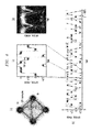
- FIG. 1 shows a prior art arrangement for measurement of the electrical field of an optical input signal S.
- optical input signal S and a reference local oscillator optical signal LO from a laser source 14 are applied as separate inputs to a 90° optical hybrid 16 .
- Optical hybrid 16 mixes optical input signal S with the four quadrature states associated with reference signal LO in the complex-field space. The operation of optical hybrid 16 therefore generates a set of four mixed fields, representing the complex field sums S+LO, S ⁇ LO, S+jLO and S ⁇ jLO, as shown.
- the pair of field sums S+LO and S ⁇ LO as applied as inputs to a first balanced detector 18 , which will generate an electrical signal output representative of the difference between the two signals.
- the pair of field sums S+jLO and S ⁇ jLO are applied as inputs to a second balanced detector 20 .
- cos( ⁇ IF t+ ⁇ S ( t )+ ⁇ LO,1 ), and I 2 ( t ) 4
- ⁇ S (t) represents the time-varying phase of optical input signal S
- the quantity ( ⁇ LO,1 ⁇ LO,2 ) represents the relative phase shift of the optical reference signal LO between the hybrid outputs.
- this induced relative phase shift will be selected to be ⁇ /2 for an optical hybrid such as optical hybrid 16 (thus termed as a “90° optical hybrid”), although in general other phase shifts may be employed, provided that they are not integral multiples of ⁇ .
- the output currents from balanced detectors 18 and 20 are then amplified by amplifiers 22 and 24 before being digitally sampled in analog-to-digital (A/D) converters 26 and 28 .
- A/D analog-to-digital
- the acquired batches of samples from I 1 (t) and I 2 (t) are applied as inputs to a signal processor 30 in order to recover a visualization of the electrical field of optical input signal S.
- the intermediate frequency will be non-zero (i.e., ⁇ IF ⁇ 0).
- the value of the IF needs to be calculated in order to extract ⁇ S (t), which represents the phase modulation of interest of the signal.
- This prior art coherent detection technique as shown in FIG. 1 requires the use of electronic sampling technology (A/D converters 26 , 28 ) and thus has at least one significant drawback associated with the bandwidth limitation of the electronic A/D converter and digital sampling circuits.
- the highest available analog bandwidth in high-speed A/D converters is today typically ⁇ 20 GHz and hence the maximum measurable signal “baud” (i.e. symbol rate) is generally less than 30 GBaud.
- optical sampling In contrast to electrical sampling, optical sampling is a proven technology that can provide extremely high bandwidth. Traditionally, optical sampling has been used to measure the time-varying optical power of an optical input signal with very high temporal resolution, but very few optical-sampling implementations are capable of measuring the complete electrical field of an optical signal.
- FIG. 2 shows an exemplary prior-art arrangement for a coherent detection linear optical sampling system that is capable of measuring the complete electrical field of the optical input signal.
- optical input signal S is mixed in an optical hybrid 36 with coherent light serving as a reference local oscillator (LO) signal originating from a pulsed sampling laser source 34 .
- LO local oscillator
- the main difference between the prior art linear sampling system in FIG. 2 and the electronic sampling system in FIG. 1 is the utilization of “pulsed” reference LO signal in the arrangement of FIG. 2 .
- a continuous wave (CW) source 14 is used in the prior-art arrangement of FIG. 1 .
- the use of a pulsed sampling laser provides a fast gating functionality that is independent of the limited bandwidth of an A/D converter. By reducing the optical-sampling rate to well below the analog bandwidth of the A/D converter, the measurement bandwidth of the system will be dictated only by the temporal resolution of the optical-sampling gate (roughly the pulse width of the pulsed source 34 ).
- the four output mixed electric-field signals from optical hybrid 36 are applied as inputs to a pair of balanced detectors 40 and 42 .
- the detector currents are then amplified by amplifiers 44 and 46 and applied as separate inputs to an A/D converter 38 .
- A/D converter 38 needs to operate at the same sampling rate as the pulse rate of the sampling laser 34 .
- a photodetector 48 and a pulser circuit 50 are coupled between sampling laser source 34 and A/D converter 38 and are used to create a clock signal that synchronizes the sampling rate of sampling laser 34 with the sampling rate of A/D converter 38 .
- the required signal processing needed in order to reconstruct the original waveform is similar to that described for the electrical sampling case in FIG. 1 and is not explicitly illustrated in FIG. 2 .
- the present invention relates to a high bandwidth optical-sampling technique with high bandwidth for systems employing advanced modulation formats and, more particularly, to a phase-sensitive sampling method accomplished by coherently mixing optical samples from a high-speed optical gate with a separate local oscillator, followed by digital signal processing of the collected samples (particularly well-suited for measurement of the electrical field of optical signals).
- an optical input signal S is first optically sampled using an optical sampling gate, where the phase characteristics of the resulting gated signal are substantially the same as optical input signal S.
- the generated optical samples are thereafter coherently mixed with a CW local oscillator (LO) signal (from a separate laser source) in a 90° optical hybrid (or other suitable phase-diverse mixing element).
- LO local oscillator
- the output fields from the 90° optical hybrid are then detected by balanced detectors and the generated photodetector currents digitized using analog-to-digital converters (ADCs) sampling synchronously with the sampling pulse source.
- ADCs analog-to-digital converters
- the described nonlinear optical sampling arrangement of a preferred embodiment of the present invention thus provides high temporal resolution sampling of the complete electrical field of an optical data signal.
- the present invention has at least one advantage over the prior-art linear sampling arrangement in that the sampling pulse source and the LO source of the present invention comprise two separate and independent optical sources.
- the wavelength of optical input signal S can be tuned without requiring the sampling pulse source wavelength to change likewise; only the CW LO source is required to track the wavelength of the generated optical samples in order to obtain a suitable IF.
- Tuning a CW LO source e.g., a single-frequency laser
- polarization-independent and polarization-diversity phase-sensitive optical sampling can be realized.
- a polarization-independent nonlinear optical sampling gate is utilized in combination with either a polarization-diversity optical-hybrid arrangement or a polarization-independent optical-hybrid arrangement.
- FIG. 1 illustrates a prior art coherent detection arrangement for electrical sampling detection of both the amplitude and phase of time varying optical signals
- FIG. 2 illustrates a prior art arrangement for linear sampling
- FIG. 3 shows an embodiment of the present invention for a four-wave mixing (FWM) based optical sampling gate used to sample the signal before coherent mixing of the optical samples with a CW LO laser in a 90-degree optical hybrid.
- the detected samples are then signal processed to visualize the input signal;
- FWM four-wave mixing
- FIG. 4 shows the results of measurements on a 10 GBaud QPSK signal using the embodiment of the present invention as shown in FIG. 3 ;
- FIG. 5 shows the results of measurements on a 40 GBaud BPSK signal using the embodiment of the present invention as shown in FIG. 3 ;
- FIG. 6 illustrates a polarization-diversity arrangement of the present invention for measurement of both orthogonal states of polarization of the optical signal under test enabling measurement of polarization multiplexed signals;
- FIG. 7 shows an embodiment of the present invention with a polarization-diversity 90° optical hybrid for a polarization diversity sampling arrangement
- FIG. 8 shows an embodiment of the present invention with a polarization independent 90 degree optical hybrid for a polarization-diversity sampling arrangement
- FIG. 9 illustrates a polarization independent arrangement of the present invention for measurement independent of the state of polarization (SOP) the optical input signal.
- SOP state of polarization
- FIG. 3 A first preferred embodiment of the present invention is illustrated in FIG. 3 .
- an optical input signal S is first optically sampled by a nonlinear sampling process performed by a sampling gate 56 .
- a sampling pulse source 58 provides a high-power optical pulse train input P, at a known repetition rate f s , to optical sampling gate 56 .
- the stream of optical sampling pulses P will interact with the electrical field of optical input signal S in a sampling process in the sampling gate 56 and thus generate optically-sampled versions O of the optical data signal field at the output of sampling gate 56 .
- the sampled version O is generated at a new wavelength ⁇ sample separated from the wavelengths, ⁇ signal and ⁇ pump , of both optical input signal S and sampling pulses P, respectively, as shown in diagram A of FIG. 3 .
- the generated streams of optical samples O can be extracted by the use of, for example, an optical passband filter (e.g., a 2 nm optical filter), shown as optical filter 60 in FIG. 3 . That is, filter 60 is selected to allow only the signal at wavelength ⁇ sample (also often referred to as the “idler” wavelength) to continue to propagate through the system.
- an optical passband filter e.g., a 2 nm optical filter
- the SOP of optical input signal S and optical sampling pulses P are preferably aligned at the input of sampling gate 56 .
- the degree of alignment may be adjusted by using a polarization controller (not shown) on optical data signal S (or sampling pulse train P) before it enters sampling gate 56 .
- a polarization controller not shown
- sampling gate 56 need not be based on a four-wave mixing process or other nonlinear process.
- the strobe pulses emitted by sampling pulse source 58 need not necessarily be optical.
- the sampling gate 56 might be an electro-absorption modulator and the “strobe pulse” from source 58 might be a very fast electrical pulse.
- sampling gate 56 might be based on a saturable-absorption process, triggered by an optical strobe pulse.
- the sampled output pulse train will have the same wavelength as the input pulse, unlike the FWM approach, where the output pulse is in general at a different (“idler”) wavelength.
- optical pulse train P need not comprise pulses having a constant temporal spacing, i.e. characterized by a single repetition rate f s , but may include any known repetitive pattern. It will be apparent to a person skilled in the art how the invention can be modified for such a case.
- Optical sampling technologies can provide extremely high bandwidth measurement capability (bandwidths greater than 500 GHz have been demonstrated) and can be implemented using a large variety of optical phenomena and hardware arrangements.
- key to the present invention is that, in addition to enabling high measurement bandwidth, the sampling technique used for optical gating within sampling gate 56 preserves the phase of optical input signal S throughout the sampling process. This preservation allows for the possibility to recover the complete electrical field of optical input signal S.
- a nonlinear sampling gate 56 uses four wave mixing (FWM) between optical sampling pulse train P and optical input signal S.
- FWM can be performed in optical fibers exhibiting nonlinear characteristics (such as, for example, highly nonlinear optical fiber (HNLF)).
- HNLF highly nonlinear optical fiber
- ⁇ is defined as the nonlinear coefficient of the HNLF
- P p is the peak power of pulse train P
- L is the length of the HNLF segment.
- large conversion efficiency is typically advantageous and in a FWM sampling gate an efficiency greater than 100% (i.e., ‘gain’) can be achieved.
- the FWM process requires optical phase matching for efficient nonlinear interaction and, as a result, the generated output field of samples has a phase that is directly dictated by the phases of optical input signal S and the field of optical sampling pulses P.
- the optical phase variation of the output optical pulse samples O generated in nonlinear sampling gate 56 can be considered to be directly representative of the phase variations of optical input signal S.
- the generated optical pulse samples O and a CW reference signal LO from a CW laser source 62 are coherently combined in an optical mixing element, preferably an optical hybrid, such as the illustrated optical hybrid 64 .
- the wavelength of reference signal LO from laser source 62 denoted ⁇ LO , is chosen to overlap the wavelength of the samples ( ⁇ samples ) generated in the sampling process, where diagram B in FIG. 3 illustrates this overlap.
- ⁇ LO The wavelength of reference signal LO from laser source 62
- ⁇ LO the wavelength of reference signal LO from laser source 62
- optical hybrid 64 functions to split and thereafter combine the two separate input signals, optical pulse samples O and CW reference signal LO, forming a set of four separate optical output signals, each signal coupled into a separate output signal path.
- each optical output signal will exhibit different relative phase shift between the optical pulse samples O and the electric field of reference signal LO.
- the relative phase shift of the four output ports of the optical hybrid 64 differs by 90° or equally ⁇ /2 radians (90° optical hybrid) yielding four output mixed fields represented by the complex field sums O+LO, O ⁇ LO, O+jLO and O ⁇ jLO. It is to be understood that there are other appropriate choices of relative delays between optical samples O and the field of CW reference signal LO and that the subject matter of the present invention is not limited to using only a 90° optical hybrid.
- optical hybrid 64 can be implemented in many different ways.
- the signal combining and splitting properties of the hybrid may be provided by an all-fiber arrangement, planar waveguide technologies, or free-space bulk optics, or a combination thereof. It is to be understood that the present invention is independent of the choice of implementation of optical hybrid 64 .
- the four output complex field sums from 90° optical hybrid 64 are then applied as inputs to a pair of balanced detectors 66 and 68 , where the samples originating from O+LO and O ⁇ LO are provided as separate inputs to balanced detector 66 and the samples originating from O+jLO and O ⁇ jLO are provided as separate inputs to balanced detector 68 .
- the square-law balanced detection of mixed samples O with reference signal LO results in that only the mixing terms between O and LO will be generated as electrical output signals i 1 (t) and i 2 (t) from balanced detectors 66 and 68 , respectively.
- the non-mixed terms are cancelled by subtraction in the balanced detection process.
- the electrical signals are thereafter applied as inputs to a pair of amplifiers (not shown) before being individually digitized in an analog-to-digital converter (ADC) 70 .
- ADC analog-to-digital converter
- the sampling rate in ADC 70 must be the same as (or a sub-multiple of) the optical sampling rate determined by the repetition rate f s of sampling pulse source 58 . Also, the time delay of the sampling process must be adjusted in order to sample each incoming electrical signal sample close to its peak value. Furthermore, the analog bandwidth of ADC 70 needs to be large enough so as to separate each electrical signal sample value, hence on the order of the optical sampling rate f s , (which may still be dramatically lower than the bandwidth of the input optical signal S).
- only two of the outputs from optical hybrid 64 are required to be detected (i.e., single-ended detection).
- the non-mixing terms of the complex field sums will remain at the output of the detectors.
- a higher LO-to-O ratio is required (compared to the balanced detection case) for correct measurements.
- all four of the outputs may be detected in a balanced detector arrangement where the non-mixing terms will drop out.
- the two streams of electrical signal samples are signal processed in order to remove the influence of the intermediate frequency (IF) between the generated samples of optical input signal S and CW reference signal LO and recover the time-varying electrical field amplitude and phase of optical input signal S.
- the relative phase can be divided into a “slow”, time-varying intermediate frequency (IF) part and a “fast” time varying phase part, originating from the data modulation of optical input signal S.
- the IF part stems from the instant frequency offset between the optical carriers of samples O and CW reference signal LO, and is removed by a signal processing algorithm implemented in signal processor 72 in order to extract the optical signal phase modulation of interest.
- signaling processing algorithms suitable for IF recovery are known in the art (see, for example, US Patent Publication 2006/0245766) and it is to be understood that the present invention is not limited to any specific signal processing implementation.
- the pair of balanced detectors 66 and 68 can be replaced by a set of four separate detectors, followed by amplification and individual analog-to-digital conversion of the four detected streams of samples.
- the balanced detection process may be emulated within signal processor 72 to produce the same functionality as when using balanced detectors.
- the present invention generates sampled information about the amplitude and phase of the optical signals electric field as a function of time.
- the present invention provides the possibility to visualize the measured signal in great detail in a variety of ways.
- the field of optical input signal S can be visualized in the complex plane as a constellation diagram, showing the superimposed optical field vectors (phasors) of the measured signal.
- FIG. 4( a ) is associated with the measurement of a 10 GBaud QPSK signal and FIG. 5( a ) is associated with the measurement of a 40 GBaud BPSK signal.
- the asynchronous sampling technique of the present invention also yields information about the signal data transitions (gray samples in the constellation diagrams).
- Constellation diagrams however, only show amplitude and phase information without time information.
- the present invention also provides timing information for each measured sample and, as a result, visualization of phase, amplitude or optical power in an eye-diagram (or data pattern form, for repetitive data modulated on optical input signal S) is also possible. It is to be understood that the present invention is independent of the choice of visualization mode of the measured electric field of optical input signal S.
- FIGS. 4( b ) and 5 ( b ) show the optical phase of the signal patterns (2 7 -1 bits) in a visualized form, with FIGS. 4( c ) and 5 ( c ) illustrating a portion of the phase patterns in greater detail, where the high temporal resolution of the measurement enables accurate measurement of the rapid phase transitions.
- FIGS. 4( d ) and 5 ( d ) show the eye-diagram of optical input signal S power for the 10 GBaud QPSK signal and 40 GBaud BPSK signals, respectively.
- FIGS. 4 and 5 are associated with B/QPSK, it is to be understood that the principles of the present invention are equally applicable to other modulation formats, including but not limited to APSK and QAM.
- the preferred implementation involves the use of optical fiber-based components.
- the present invention can also be implemented using free-space optics in bulk optical components, monolithic waveguide optical components or a mix of different types of free-space and guided-wave components.
- FIG. 3 illustrates an exemplary polarization diversity arrangement which may utilized in the practice of the present invention.
- optical input signal S (which is in general of random polarization) is first applied as an input to a polarization separation element, such as a polarization beam splitter (PBS) 74 , which decomposes optical input signal S to form a pair of polarized output signals denoted S x and S y .
- PBS polarization beam splitter
- each of these polarized signals are separately processed through a pair of separate sampling arrangements illustrated in FIG. 3 and discussed hereinabove.
- the functionality of polarization-independent measurements of optical input signal S can be accomplished by thereafter combining the measured field components into a replication of the original electric field of the input optical signal.
- the signal processing part of the invention responsible for IF recovery can be performed either on the combined measured samples from the two sampling arrangements, or in a separate fashion on each of the two sets of samples.
- the recovery of the two orthogonal polarization parts of the polarization-multiplexed optical input signal can be performed in different ways.
- the input SOP of optical input signal S may be adjusted (such as by means of a polarization controller, not shown) such that the S x and S y components directly represent a pair of orthogonally-polarized data-carrying signals.
- IF recovery in the signal processing part of the present invention is independently performed in each of the two branches show in FIG. 6 .
- the SOP of optical input signal S is suitably adjusted, it is also possible to measure S x and S y in a single arrangement of the present invention illustrated in FIG. 3 by including (for example) an optical 2-to-1 switch after the PBS 74 to toggle between measurements of S x and S y .
- an optical 2-to-1 switch after the PBS 74 to toggle between measurements of S x and S y .
- the two orthogonal polarization parts of the polarization-multiplexed optical input signal S can then be recovered and separated visualized.
- the SOP of optical input signal S is not aligned; the two orthogonal polarization parts of the polarization-multiplexed signal are then sampled individually and in this case the recovery can be included in the signal processing part of the inventive arrangement, using the combined information of the two branches as inputs to known algorithms.
- the LO reference laser and the optical sampling pulse source used in the embodiment as shown in FIG. 3 can be reused for measurement of both S x and S y .
- one alternative embodiment utilizes coarse time gating of the optical signal before polarization beam splitter 74 .
- the coarse time gating is responsible for extracting parts of the optical signal with durations related to the optical sampling rate and the number of samples measured for each characterization of the electric field of the optical signal. Following each extracted part of the optical signal, the optical signal must be removed with high extinction ratio for a duration related to the duration of the extracted part of the optical signal.
- the outputs from polarization beam splitter 74 can then, by using delay means and optical coupling means, be time-interleaved into a single sampling arrangement according to FIG. 3 .
- Polarization-diversity measurements can also be accomplished by the alternative embodiment of the present invention as illustrated in FIG. 7 .
- the utilization of a polarization independent optical sampling gate 76 eliminates the need to align the SOP of optical input signal S with the SOP of optical sampling gate 76 .
- two separate, orthogonally-polarized and independent sampling paths are created within the same sampling gate 76 . This is accomplished by launching orthogonally polarized sampling pulse streams P x and P y through sampling gate 76 , which independently opens a sampling window which is co-polarized with the SOP of the incoming sampling pulses. By virtue of using this pair of sampling pulses, a pair of orthogonal optical pulse streams O x and O y are created at the output of sampling gate 76 , as shown.
- the orthogonally polarized samples O x and O y are thereafter mixed with a CW reference signal LO from a separate laser source 78 in a polarization diversity optical hybrid 80 .
- the orthogonally polarized samples, O x and O y are mixed separately with CW reference signal LO so that the mixed terms O+LO, O ⁇ LO, O+jLO, and O ⁇ jLO for each of the orthogonal polarizations appears as individual outputs from optical hybrid 80 .
- the set of eight mixed output samples are presented in pairs to a group of four balanced detectors, creating a set of four electrical output signals.
- inputs O x +LO x and O X ⁇ LO X are applied as inputs to a first balanced detector 82
- inputs O x +jLO x and O x ⁇ jLO x are applied as inputs to a second balanced detector 84
- Input mixed samples O y +LO y and O y ⁇ LO y are applied as inputs to a third balanced detector 86 in similar fashion, with inputs O y +jLO y and O y ⁇ jLO y applied as inputs to a fourth balanced detector 88 .
- the set of four electrical signals are thereafter applied as inputs to a four-channel ADC 90 which digitizes the signals and presents them as an input to signal processor 92 which performs the desired measurements required for signal visualization.
- FIG. 8 An alternative configuration of the polarization-diverse arrangement of the present invention is shown in FIG. 8 .
- the polarization diversity is accomplished by the utilization of a polarization independent optical hybrid 94 in conjunction with polarization independent optical sampling gate 76 .
- the SOP of reference signal LO from laser source 78 should be aligned such that the field components of signal LO split equally in amplitude with respect to the SOPs of O x and O y .
- two coherently mixed optical samples with orthogonal polarization states will be present at each output of optical hybrid 94 .
- the orthogonally polarized samples are thereafter separated by means of a set of polarization beam splitters 96 , 98 , 100 , 102 .
- the outputs from PBS elements 96 - 102 are thereafter converted into electrical signals through the set of balanced detectors 82 , 84 , 86 and 88 and individually digitized within an ADC 90 in pairs corresponding to S+LO and S ⁇ LO (S+jLO and S ⁇ jLO) for each orthogonally polarized sample of optical input signal S.
- the signal processing part of the invention is the same as for the arrangement illustrated in FIG. 6 .
- Polarization-independent measurements can be accomplished by the alternative embodiment of the present invention illustrated in FIG. 9 .
- no polarization beam splitters are present at the output of polarization independent optical hybrid 94 .
- the orthogonally-polarized, mixed samples at the outputs of polarization independent optical hybrid 94 are not separated and cannot be individually transformed into electrical signals. Instead, as shown in FIG. 9 , the orthogonally polarized samples at each output are applied as inputs to the same balanced photodetector.
- the energy of the samples can be integrated by the detection means to provide polarization-independent measurements. This is similar to what is done in the polarization-independent intensity sampling arrangement described in U.S. Pat. No. 7,199,870, herein incorporated by reference.
- the orthogonally-polarized samples on each output of the hybrid should have the same phase relation to CW reference signal LO, e.g. the orthogonally-polarized samples should experience constructive (destructive) interference at the same time.
- the relative phase of the equal-amplitude field components from laser source 78 being mixed with the orthogonally-polarized samples O x and O y in polarization independent optical hybrid 94 has to be controlled to accomplish this. Digitizing and signal processing of the polarization-independent measurements can be performed according to previous arrangements.
- the relative phase requirement between the orthogonally-polarized optical samples and the orthogonally-polarized components of CW reference signal LO is met by controlling the relative phase of the two orthogonally-polarized optical samples as applied as inputs to optical hybrid 94 .
- the relative phase requirement between the orthogonally-polarized optical samples and the orthogonally-polarized components of the LO is met by controlling the relative phase of the two orthogonally polarized sampling pulses P x and P y from sampling pulse source 96 .
- the relative phase requirement between the orthogonally-polarized optical samples and the orthogonally-polarized components of the LO is met by controlling the input SOP of the LO into optical hybrid 94 .
- time-base In order to visualize the measured electric field of optical input signal S in a way that requires timing information for each sample O (e.g., an eye-diagram or data pattern visualization), a method to obtain the time-base must be used.
- time-base designs including hardware triggered sequential sampling techniques, software based sequential sampling techniques, and real-time sampling techniques to name a few.
- the present invention can be implemented using many different time-base designs, as long as the sampling rate is high enough for IF recovery. New algorithms for IF recovery appear constantly, and hence a minimum sampling rate for a certain IF cannot be specified. Nevertheless, an example of such IF recovery algorithm can be found in US2006/0245766 A1. It is also to be noted that for constellation diagram visualization of the electrical field of the optical signal, no time-base is needed (since the constellation diagrams do not include timing information).
Landscapes
- Physics & Mathematics (AREA)
- Electromagnetism (AREA)
- Engineering & Computer Science (AREA)
- Computer Networks & Wireless Communication (AREA)
- Signal Processing (AREA)
- Photometry And Measurement Of Optical Pulse Characteristics (AREA)
Abstract
Description
I 1(t)=4|S(t)∥LO|cos(ωIF t+φ S(t)+φLO,1), and
I 2(t)=4|S(t)∥LO|cos(ωIF t+φ S(t)+φLO,2),
where the intermediate frequency IF related term ωIF is defined as ωS−ωLO, which is the angular frequency difference between the signal field and the LO field. The term φS(t) represents the time-varying phase of optical input signal S, and the quantity (φLO,1−φLO,2) represents the relative phase shift of the optical reference signal LO between the hybrid outputs. Advantageously, this induced relative phase shift will be selected to be π/2 for an optical hybrid such as optical hybrid 16 (thus termed as a “90° optical hybrid”), although in general other phase shifts may be employed, provided that they are not integral multiples of π.
η=(γP p L)2,
where γ is defined as the nonlinear coefficient of the HNLF, Pp is the peak power of pulse train P and L is the length of the HNLF segment. Indeed, large conversion efficiency is typically advantageous and in a FWM sampling gate an efficiency greater than 100% (i.e., ‘gain’) can be achieved.
Claims (19)
Priority Applications (1)
| Application Number | Priority Date | Filing Date | Title |
|---|---|---|---|
| US12/710,683 US8280245B2 (en) | 2009-02-23 | 2010-02-23 | Optical sampling with coherent detection |
Applications Claiming Priority (2)
| Application Number | Priority Date | Filing Date | Title |
|---|---|---|---|
| US20841809P | 2009-02-23 | 2009-02-23 | |
| US12/710,683 US8280245B2 (en) | 2009-02-23 | 2010-02-23 | Optical sampling with coherent detection |
Publications (2)
| Publication Number | Publication Date |
|---|---|
| US20100215357A1 US20100215357A1 (en) | 2010-08-26 |
| US8280245B2 true US8280245B2 (en) | 2012-10-02 |
Family
ID=42631049
Family Applications (1)
| Application Number | Title | Priority Date | Filing Date |
|---|---|---|---|
| US12/710,683 Active 2031-01-29 US8280245B2 (en) | 2009-02-23 | 2010-02-23 | Optical sampling with coherent detection |
Country Status (1)
| Country | Link |
|---|---|
| US (1) | US8280245B2 (en) |
Cited By (1)
| Publication number | Priority date | Publication date | Assignee | Title |
|---|---|---|---|---|
| US20120321325A1 (en) * | 2011-06-14 | 2012-12-20 | Ciena Corporation | Parallel conversion between optical and digital |
Families Citing this family (10)
| Publication number | Priority date | Publication date | Assignee | Title |
|---|---|---|---|---|
| US8768180B2 (en) * | 2009-02-23 | 2014-07-01 | Exfo, Inc. | All-optical, phase sensitive optical signal sampling |
| US8923707B2 (en) * | 2010-06-14 | 2014-12-30 | Infinera Corporation | Apparatus for compensating optical signal impairments |
| US8922771B2 (en) | 2011-10-31 | 2014-12-30 | Northrop Grumman Systems Corporation | Multichannel polarization stabilizer |
| US8922772B2 (en) | 2011-10-31 | 2014-12-30 | Northrop Grumman Systems Corporation | Multichannel polarization stabilization employing synchronous phase-locking methods |
| US9209908B2 (en) * | 2012-10-04 | 2015-12-08 | Zte (Usa) Inc. | System and method for heterodyne coherent detection with optimal offset |
| US20150050032A1 (en) * | 2013-08-13 | 2015-02-19 | Alcatel-Lucent Usa, Inc. | Digitally locking coherent receiver and method of use thereof |
| EP3200363B1 (en) * | 2016-01-27 | 2019-10-02 | Alcatel Lucent | Linear optical sampling system and coherent detection of an optical signal |
| CN107402029B (en) * | 2017-08-08 | 2019-08-20 | 电子科技大学 | Method and system for improving measurement speed of distributed optical fiber sensing using orthogonal signals |
| CN108712358A (en) * | 2018-04-11 | 2018-10-26 | 北京航天长征飞行器研究所 | A kind of general QAM and APSK demodulators and demodulation method |
| CN109039462B (en) * | 2018-07-19 | 2020-04-03 | 中国科学院西安光学精密机械研究所 | Multi-modulation format compatible high-speed laser signal phase-lock-free receiving system and method |
Citations (7)
| Publication number | Priority date | Publication date | Assignee | Title |
|---|---|---|---|---|
| US20040114939A1 (en) * | 2002-12-11 | 2004-06-17 | Taylor Michael George | Coherent optical detection and signal processing method and system |
| US7042629B2 (en) * | 2004-02-19 | 2006-05-09 | Lucent Technologies Inc. | Linear optical sampling method and apparatus |
| US20060245766A1 (en) * | 2005-04-29 | 2006-11-02 | Taylor Michael G | Phase estimation for coherent optical detection |
| US7133135B2 (en) * | 2004-02-20 | 2006-11-07 | Lucent Technologies, Inc. | Method and apparatus for the direct characterization of the phase of an optical signal |
| US20070041728A1 (en) * | 2005-05-13 | 2007-02-22 | Dorrer Christophe J | Method and apparatus for characterizing the electric field of periodic and non-periodic optical signals |
| US20090047030A1 (en) * | 2007-08-16 | 2009-02-19 | Fujitsu Limited | Coherent light receiving system |
| US20110019994A1 (en) * | 2009-07-27 | 2011-01-27 | Finisar Australia Pty Ltd | High Bandwidth Demodulator System And Method |
-
2010
- 2010-02-23 US US12/710,683 patent/US8280245B2/en active Active
Patent Citations (9)
| Publication number | Priority date | Publication date | Assignee | Title |
|---|---|---|---|---|
| US20040114939A1 (en) * | 2002-12-11 | 2004-06-17 | Taylor Michael George | Coherent optical detection and signal processing method and system |
| WO2004054138A2 (en) | 2002-12-11 | 2004-06-24 | Taylor Michael G | Coherent optical detection and signal processing method and system |
| US7042629B2 (en) * | 2004-02-19 | 2006-05-09 | Lucent Technologies Inc. | Linear optical sampling method and apparatus |
| US7133135B2 (en) * | 2004-02-20 | 2006-11-07 | Lucent Technologies, Inc. | Method and apparatus for the direct characterization of the phase of an optical signal |
| US20060245766A1 (en) * | 2005-04-29 | 2006-11-02 | Taylor Michael G | Phase estimation for coherent optical detection |
| US20070041728A1 (en) * | 2005-05-13 | 2007-02-22 | Dorrer Christophe J | Method and apparatus for characterizing the electric field of periodic and non-periodic optical signals |
| US7298489B2 (en) * | 2005-05-13 | 2007-11-20 | Lucent Technologies Inc. | Method and apparatus for characterizing the electric field of periodic and non-periodic optical signals |
| US20090047030A1 (en) * | 2007-08-16 | 2009-02-19 | Fujitsu Limited | Coherent light receiving system |
| US20110019994A1 (en) * | 2009-07-27 | 2011-01-27 | Finisar Australia Pty Ltd | High Bandwidth Demodulator System And Method |
Cited By (2)
| Publication number | Priority date | Publication date | Assignee | Title |
|---|---|---|---|---|
| US20120321325A1 (en) * | 2011-06-14 | 2012-12-20 | Ciena Corporation | Parallel conversion between optical and digital |
| US8761614B2 (en) * | 2011-06-14 | 2014-06-24 | Ciena Corporation | Parallel conversion between optical and digital |
Also Published As
| Publication number | Publication date |
|---|---|
| US20100215357A1 (en) | 2010-08-26 |
Similar Documents
| Publication | Publication Date | Title |
|---|---|---|
| US8280245B2 (en) | Optical sampling with coherent detection | |
| US8768180B2 (en) | All-optical, phase sensitive optical signal sampling | |
| US7110677B2 (en) | Method and system for optical time division multiplexed fiber communications with coherent detection | |
| Clark et al. | Performance of a time-and wavelength-interleaved photonic sampler for analog-digital conversion | |
| CA2419357C (en) | Polarization scrambler and optical network using the same | |
| US20090009772A1 (en) | Optical measuring apparatus and optical measuring method | |
| Schmidt-Langhorst et al. | Optical sampling techniques | |
| Sköld et al. | All-optical waveform sampling in high-speed optical communication systems using advanced modulation formats | |
| Raybon et al. | 160-Gbaud coherent receiver based on 100-GHz bandwidth, 240-GS/s analog-to-digital conversion | |
| CN106019767B (en) | The time-interleaved optical analog to digital conversion device of polarization-maintaining | |
| JP2019161246A (en) | Digital coherent transmission system | |
| EP2709295A1 (en) | Visualisation of an optical signal by linear optical sampling | |
| WO2010033654A2 (en) | All-optical balanced detection system | |
| Awad et al. | Subharmonic optical clock recovery from 160 Gb/s using time-dependent loss saturation inside a single electroabsorption modulator | |
| Westlund et al. | All-optical phase-sensitive waveform sampling at 40 GSymbol/s | |
| US20060120483A1 (en) | Heterodyne-based optical spectrum analysis using data clock sampling | |
| US7149029B1 (en) | Interferometric PPM demodulators based on semiconductor optical amplifiers | |
| WO2012172309A1 (en) | Optical signal processing | |
| Dorrer et al. | High-sensitivity high-resolution sampling using linear optics and waveguide optical hybrid | |
| JP2010025669A (en) | Optical sampling apparatus | |
| US20070111111A1 (en) | Light measurement apparatus and light measurement method | |
| Fan et al. | Polarization maintaining fibre loop mirror for NRZ-to-PRZ conversion in all-optical clock recovery | |
| Scott et al. | Continuous, real-time, full-field waveform measurements via spectral slicing and parallel digital coherent detection | |
| EP4228172B1 (en) | Method for an arbitrary waveform measurement and a system to operate said method | |
| WO2003036834A1 (en) | Method and system for optical time division multiplexed fiber communications with coherent detection |
Legal Events
| Date | Code | Title | Description |
|---|---|---|---|
| AS | Assignment |
Owner name: EXFO, INC., CANADA Free format text: ASSIGNMENT OF ASSIGNORS INTEREST;ASSIGNORS:WESTLUND, MATHIAS;SKOLD, MATS;SUNNERUD, HENRIK;AND OTHERS;REEL/FRAME:025979/0775 Effective date: 20110301 |
|
| STCF | Information on status: patent grant |
Free format text: PATENTED CASE |
|
| FPAY | Fee payment |
Year of fee payment: 4 |
|
| AS | Assignment |
Owner name: NATIONAL BANK OF CANADA, CANADA Free format text: SECURITY INTEREST;ASSIGNOR:EXFO INC.;REEL/FRAME:045470/0202 Effective date: 20180131 |
|
| MAFP | Maintenance fee payment |
Free format text: PAYMENT OF MAINTENANCE FEE, 8TH YEAR, LARGE ENTITY (ORIGINAL EVENT CODE: M1552); ENTITY STATUS OF PATENT OWNER: LARGE ENTITY Year of fee payment: 8 |
|
| MAFP | Maintenance fee payment |
Free format text: PAYMENT OF MAINTENANCE FEE, 12TH YEAR, LARGE ENTITY (ORIGINAL EVENT CODE: M1553); ENTITY STATUS OF PATENT OWNER: LARGE ENTITY Year of fee payment: 12 |
|
| AS | Assignment |
Owner name: NATIONAL BANK OF CANADA, CANADA Free format text: SECURITY INTEREST;ASSIGNORS:EXFO INC. (A CORPORATION RESULTING FROM THE AMALGAMATION OF 11172239 CANADA INC. AND EXFO INC.);ONTOLOGY-PARTNERS LIMITED;REEL/FRAME:072338/0500 Effective date: 20210917 |