US8232203B2 - Methods of manufacturing memory devices - Google Patents
Methods of manufacturing memory devices Download PDFInfo
- Publication number
- US8232203B2 US8232203B2 US12/763,861 US76386110A US8232203B2 US 8232203 B2 US8232203 B2 US 8232203B2 US 76386110 A US76386110 A US 76386110A US 8232203 B2 US8232203 B2 US 8232203B2
- Authority
- US
- United States
- Prior art keywords
- layer
- dielectric layer
- conductive
- patterned
- forming
- Prior art date
- Legal status (The legal status is an assumption and is not a legal conclusion. Google has not performed a legal analysis and makes no representation as to the accuracy of the status listed.)
- Expired - Fee Related, expires
Links
Images


Classifications
-
- H—ELECTRICITY
- H10—SEMICONDUCTOR DEVICES; ELECTRIC SOLID-STATE DEVICES NOT OTHERWISE PROVIDED FOR
- H10W—GENERIC PACKAGES, INTERCONNECTIONS, CONNECTORS OR OTHER CONSTRUCTIONAL DETAILS OF DEVICES COVERED BY CLASS H10
- H10W20/00—Interconnections in chips, wafers or substrates
- H10W20/01—Manufacture or treatment
- H10W20/071—Manufacture or treatment of dielectric parts thereof
- H10W20/081—Manufacture or treatment of dielectric parts thereof by forming openings in the dielectric parts
- H10W20/089—Manufacture or treatment of dielectric parts thereof by forming openings in the dielectric parts using processes for implementing desired shapes or dispositions of the openings, e.g. double patterning
-
- H—ELECTRICITY
- H10—SEMICONDUCTOR DEVICES; ELECTRIC SOLID-STATE DEVICES NOT OTHERWISE PROVIDED FOR
- H10B—ELECTRONIC MEMORY DEVICES
- H10B41/00—Electrically erasable-and-programmable ROM [EEPROM] devices comprising floating gates
- H10B41/30—Electrically erasable-and-programmable ROM [EEPROM] devices comprising floating gates characterised by the memory core region
- H10B41/35—Electrically erasable-and-programmable ROM [EEPROM] devices comprising floating gates characterised by the memory core region with a cell select transistor, e.g. NAND
-
- H—ELECTRICITY
- H10—SEMICONDUCTOR DEVICES; ELECTRIC SOLID-STATE DEVICES NOT OTHERWISE PROVIDED FOR
- H10W—GENERIC PACKAGES, INTERCONNECTIONS, CONNECTORS OR OTHER CONSTRUCTIONAL DETAILS OF DEVICES COVERED BY CLASS H10
- H10W20/00—Interconnections in chips, wafers or substrates
- H10W20/01—Manufacture or treatment
- H10W20/031—Manufacture or treatment of conductive parts of the interconnections
- H10W20/056—Manufacture or treatment of conductive parts of the interconnections by filling conductive material into holes, grooves or trenches
-
- H—ELECTRICITY
- H10—SEMICONDUCTOR DEVICES; ELECTRIC SOLID-STATE DEVICES NOT OTHERWISE PROVIDED FOR
- H10W—GENERIC PACKAGES, INTERCONNECTIONS, CONNECTORS OR OTHER CONSTRUCTIONAL DETAILS OF DEVICES COVERED BY CLASS H10
- H10W20/00—Interconnections in chips, wafers or substrates
- H10W20/01—Manufacture or treatment
- H10W20/071—Manufacture or treatment of dielectric parts thereof
- H10W20/081—Manufacture or treatment of dielectric parts thereof by forming openings in the dielectric parts
Definitions
- the present invention generally relates to a method of fabricating a memory device and, more particularly, to a method of fabricating a NAND flash device.
- a common-source-line contact may be disposed beside NAND strings for source line pick-up, while a plurality of drain contacts and bit-line contact plugs may be disposed for electrically coupling a common drain region of the NAND strings with the bit lines.
- each of the bit-line contact plugs is required to overlay and vertically aligned with a corresponding one of the drain contacts, and hence a complex lithography process may be needed.
- mis-alignment between the bit-line contact plugs (also termed “via0”) and the drain contacts (also termed “contact”) may occur, as will be discussed below.
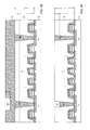
- FIGS. 1A to 1J are schematic cross-sectional views illustrating a method of manufacturing a NAND flash device in prior art. Throughout FIGS. 1A to 1J , only parts of the NAND flash device are shown for simplicity.
- a substrate 10 may be provided.
- a first dielectric layer 12 with a height T 1 may be formed on the NAND string 11 , the source select gate 112 , the drain select gate 113 , the common source region 11 a and the common drain region 11 b by a deposition process.
- the first dielectric layer 12 may include a dielectric material such as silicon oxide (SiO 2 ) or silicon oxynitride (SiON).
- a patterned first mask layer 13 of photo-resist with a first opening 131 and a plurality of second openings 132 may be formed on the first dielectric layer 12 .
- the first opening 131 may extend in a second reference direction, i.e., a direction perpendicular to the plane of the page of the diagram of FIG. 1A .
- the second openings 132 may be arranged in an array extending in the second reference direction.
- a first trench 121 and a plurality of first holes 122 may be formed into the first dielectric layer 12 through the first opening 131 and the second openings 132 , respectively, by a dry etch process using the patterned first mask layer 13 as a mask. After the trench-forming process, the patterned first mask layer 13 may then be removed by a strip process.
- a conductive material such as tungsten (W) may be deposited on the surface of the first dielectric layer 12 , the first trench 121 and the first holes 122 by a chemical vapor deposition (CVD) process, filling the first trench 121 to form a first contact structure 141 and filling the first holes 142 to form a plurality of second contact structures 142 .
- the first contact structure 141 and each of the second contact structures 142 may have a height equal to T 1 .
- a first conductive layer 14 of the conductive material may then be formed thereon.
- the first conductive layer 14 may be removed by a chemical-mechanical polish (CMP) process using the first dielectric layer 12 as a polish-stopping layer, exposing top of the first contact structure 141 and top of the second contact structures 142 .
- CMP chemical-mechanical polish
- a second dielectric layer 15 with a height T 2 may be formed on the first dielectric layer 12 by a deposition process.
- the second dielectric layer 15 may include the same dielectric material as the first dielectric layer 12 , and hence the second dielectric layer 15 may then be merged with the first dielectric layer 12 to form a third dielectric layer 16 , as shown in FIG. 1F .
- the third dielectric layer 16 may serve as an inter layer dielectric (ILD) layer.
- ILD inter layer dielectric
- a patterned second mask layer 17 of photoresist with a plurality of third openings 171 may be formed on the third dielectric layer 16 by a lithography process.
- the third openings 171 may be arranged in an array extending in the second reference direction.
- Each of the third openings 171 is vertically aligned with a corresponding one of the second contact structures 142 .
- the critical dimension of each of the third openings 171 is smaller than that of the top surface of each of the second contact structures 142 .
- a plurality of second holes 161 may be formed into the third dielectric layer 16 through the third openings 171 by a dry etch process using the patterned second mask layer 17 as a mask. Since the third openings 171 with a smaller critical dimension are vertically aligned with the second contact structures 142 , each of the second holes 161 may expose a portion of a corresponding one of the second contact structures 142 . After the hole-forming process, the patterned second mask layer 17 may then be removed.
- a conductive material same as that of the first conductive layer 14 may be deposited on the third dielectric layer 16 , filling the second holes 161 to form a plurality of third contact structures 181 .
- Each of the third contact structures 181 may have a height equal to T 2 and may overlay the corresponding one of the second contact structures 142 .
- a second conductive layer 18 of the conductive material may then be formed on the third dielectric layer 16 .
- the second conductive layer 18 may be removed by a CMP process using the third dielectric layer 16 as a polish-stopping layer. Top of the third contact structures 181 may be exposed thereafter.
- a patterned metal layer 19 may be formed on the third dielectric layer 16 and the third contact structures 181 .
- the patterned metal layer 19 may include bit lines extending in parallel in the first reference direction.
- Each of the third contact structures 181 may serve as a bit-line contact plug, which electrically couples one of the second contact structures 142 to one of the bit lines, while each of the second contact structures 142 may serve as a drain contact, which electrically couples the corresponding bit-line contact plug to the common drain region 11 b .
- the first contact structure 141 which is electrically coupled with the common source region 11 a may serve as a common-source line contact for source line pick-up.
- the critical dimensions of the third openings 171 and the third contact structures 181 may be so small that process window will be a concern without high-resolution exposure tool.
- the third contact structures 181 and the second contact structures 142 are formed by two individual steps, which may increase the risk of mis-alignment without high-precision exposure tool. It may therefore be desirable to have a method that is able to manufacture semiconductor memory devices in a simplified process and alleviate the mis-alignment issue.
- the present invention is directed to a method for manufacturing a NAND flash device that may simplify the lithography processes and avoid the mis-alignment issue.
- Examples of the present invention may provide a method of manufacturing a memory device.
- the method includes providing a substrate, forming a number of memory sectors on the substrate, wherein each of the memory sectors is coupled to an adjacent one via a first diffused region in the substrate and is coupled to another adjacent one via at least one second diffused region in the substrate, forming a first dielectric layer on the memory sectors, forming a first conductive structure through the first dielectric layer to the first diffused region, and at least one second conductive structure through the first dielectric layer to the at least one second diffused region, forming a patterned first mask layer on the first dielectric layer, the first conductive structure and the at least one second conductive structure, the patterned first mask layer exposing the first conductive structure, and etching back the first conductive structure.
- Some examples of the present invention may also provide a method of manufacturing a memory device.
- the method includes providing a substrate, forming a number of memory sectors on the substrate, wherein each of the memory sectors is coupled to an adjacent one via a first diffused region in the substrate and is coupled to another adjacent one via at least one second diffused region in the substrate, forming a first dielectric layer on the memory sectors, forming a first opening through the first dielectric layer, exposing the first diffused region, and at least one second opening through the first dielectric layer, exposing the at least one second diffused region, forming a first conductive layer on the first dielectric layer, the first conductive layer filling the first opening, resulting in a first conductive structure, and filling the at least one second opening, resulting in at least one second conductive structure, forming a patterned first mask layer on the first conductive layer, the patterned first mask layer exposing a portion of the first conductive layer over the first conductive structure, etching back the exposed portion of the first conductive layer, and
- Examples of the present invention may further provide a method of manufacturing a memory device.
- the method includes providing a substrate, forming a number of memory sectors on the substrate, wherein each of the memory sectors is coupled to an adjacent one via a first diffused region in the substrate and is coupled to another adjacent one via at least one second diffused region in the substrate, forming a first dielectric layer on the memory sectors, forming a first opening through the first dielectric layer, exposing the first diffused region, and at least one second opening through the first dielectric layer, exposing the at least one second diffused region, forming a first conductive layer on the first dielectric layer, the first conductive layer filling the first opening, resulting in a first conductive structure, and filling the at least one second opening, resulting in at least one second conductive structure, forming a patterned first mask layer on the first conductive layer, the patterned first mask layer exposing a portion of the first conductive layer over the first conductive structure, and etching back the first conductive structure through the exposed portion of the first
- FIGS. 1A to 1J are schematic cross-sectional views illustrating a method of fabricating a NAND flash device in prior art
- FIGS. 2A to 2P are schematic cross-sectional views illustrating a method of fabricating a NAND flash device in accordance with an example of the present invention
- FIG. 3 is a schematic three-dimensional view of the NAND flash device in part fabricated by the method illustrated in FIG. 2P ;
- FIGS. 4A to 4F are schematic cross-sectional views illustrating a method of fabricating a NAND flash device in accordance with another example of the present invention.
- FIGS. 5A to 5D are schematic cross-sectional views illustrating a method of fabricating a NAND flash device in accordance with yet another example of the present invention.
- FIGS. 6A to 6D are schematic cross-sectional views illustrating a method of fabricating a NAND flash device in accordance with still another example of the present invention.
- FIGS. 7A and 7B are schematic cross-sectional views illustrating a method of fabricating a NAND flash device in accordance with an example of the present invention.
- FIGS. 8A and 8B are schematic cross-sectional views illustrating a method of fabricating a NAND flash device in accordance with another example of the present invention.
- FIGS. 2A to 2P are schematic cross-sectional views illustrating a method of fabricating a NAND flash device 3 in accordance with an example of the present invention. Throughout FIGS. 2A to 2P , only parts of the NAND flash device 3 are shown for simplicity. In addition to the exemplary NAND flash devices, the method according to the present invention may be applicable to the manufacturing of other semiconductor memory devices where mismatch between contact and via0 may concern.
- a substrate 30 that has been doped with, for example, a p-type impurity may be provided.
- a cell array of the NAND flash device 3 may be formed on the substrate 30 .
- the cell array may include a number of units each further including a control gate layer 3 a , a control gate oxide layer 3 b , a floating gate layer 3 c and a floating gate oxide layer 3 d .
- Spacers 3 e maybe formed along the sides of the gate structure to provide electrical isolation from adjacent units of the cell array.
- source and drain regions may be formed in the substrate 30 by, for example, an implantation followed by a diffusion process.
- the units of the cell array may extend in a first reference direction such as a row direction, and may be coupled with each other in series.
- unit 311 may be coupled to unit 312 via a diffused region including a source region 311 a and a drain region 312 b , and coupled to unit 313 via another diffused region including a drain region 311 b and a source region 313 a .
- source and drain regions may be interchangeable, depending on the voltages applied thereto.
- a row of the serially coupled units of the cell array may be grouped as a NAND string 31 .
- a source select gate 314 and a drain select gate 315 may be formed on each side of the NAND string 31 .
- the drain region 314 b of the source select gate 314 may be electrically coupled with the source region 312 a of the unit 312 of the NAND string 31
- the source region 314 a of the source select gate 314 may be electrically coupled with the source region 316 a of a source select gate 316 of another NAND string (not shown) immediately adjacent to the NAND string 31 on one side in the same row.
- the diffused region including the source regions 314 a and 316 a is called a common source region 31 a.
- the source region 315 a of the drain select gate 315 may be electrically coupled with the drain region 313 b of the unit 313 of the NAND string 31
- the drain region 315 b of the drain select gate 315 may be electrically coupled with the drain region 317 b of a drain select gate 317 of another NAND string (not shown) immediately adjacent to the NAND string 31 on the other side.
- the diffused region including the drain regions 315 b and 317 b is called a common drain region 31 b.
- a first dielectric layer 32 may be formed on the cell array including the NAND string 31 between the source select gate 314 and the drain select gate 315 by, for example, a deposition process.
- the first dielectric layer 32 may include a dielectric material such as silicon oxide (SiO 2 ) or silicon oxynitride (SiON) with a thickness T 0 .
- T 0 may be equal to T 1 plus T 2 , wherein T 1 represents the height of the common-source-line contact, while T 2 represents the height of the bit-line contact plug of the NAND flash device manufactured by the conventional method illustrated in FIG. 1F .
- a first mask layer 33 may be formed on the first dielectric layer 32 by a coating process.
- the first mask layer 33 may include photoresist.
- a patterned first mask layer 33 - 1 may be formed by a lithography process.
- the patterned first mask layer 33 - 1 may expose portions 321 and 322 of the first dielectric layer 32 through a first opening 331 a and a plurality of second openings 332 a .
- the first opening 331 a may extend in a second reference direction such as a column direction, while the second openings 322 a may be arranged in a column in the second direction.
- a first trench 323 and a plurality of holes 324 may be formed into the first dielectric layer 32 through the exposed portions 321 and 322 , respectively, by a dry etch process, which uses the patterned first mask layer 33 - 1 as a mask.
- the first trench 323 may extend in the second reference direction and, due to the nature of dry etching, may be tapered from the exposed portion 321 of the patterned first mask layer 33 - 1 to the common source region 31 a , exposing portions 31 a 1 of the common source region 31 a.
- the holes 324 may be tapered from the exposed portions 322 of the patterned first mask layer 33 - 1 to the common drain region 31 b , exposing portions 31 b 1 of the common drain region 31 b.
- the patterned first mask layer 33 - 1 may be removed by a strip process.
- a conductive layer 34 may be formed on the first dielectric layer 32 , filling the first trench 323 and the holes 324 , by a deposition process such as a CVD process.
- the conductive layer 34 may include tungsten (W).
- the first trench 323 and the holes 324 filled with the conductive material form a first contact structure 331 and a plurality of second contact structures 332 , respectively.
- the conductive layer 34 on the first dielectric layer 32 may then be removed by a chemical-mechanical polish (CMP) process, using the first dielectric layer 32 as a polish-stopping layer. Top of the first contact structure 331 and second contact structures 332 may then be exposed.
- CMP chemical-mechanical polish
- a second mask layer 35 may be formed on the first dielectric layer 32 .
- the second mask layer 35 may include photoresist.
- a patterned second mask layer 35 - 1 may be formed on the first dielectric layer 32 , exposing the first contact structure 331 and portions 325 of the first dielectric layer 32 around the first contact structure 331 through a third opening 351 .
- the third opening 351 may extend in the second reference direction.
- the dimension of the third opening 351 may be substantially greater than that of the third opening 171 in the conventional method illustrated in FIG. 1 F so that the lithography process for forming the third openings 351 may be simplified or require less resolution and precise exposure tool.
- a second trench 326 may be formed into the first contact structure 331 through the exposed top thereof by a dry etch process, which uses the patterned second mask layer 35 - 1 as a mask. By controlling the time of the dry etch process, the first contact structure 331 may be etched back to a desired level so that the second trench 326 may have a depth equal to T 2 .
- the patterned second mask layer 35 - 1 may be removed by a strip process.
- a second dielectric layer 36 may be formed on the first dielectric layer 32 by a deposition process, filling the second trench 326 .
- the second dielectric layer 36 may include a dielectric material same as that of the first dielectric layer 32 . Due to the second trench 326 , a shallow trench 361 may exist in the top surface of the second dielectric layer 36 .
- a third dielectric layer 37 composed of the first and second dielectric layers 32 and 36 may thus be defined.
- the third dielectric layer 37 may be reduced in height by a CMP process using the second contact structure 332 as a polish-stopping layer, exposing top of the second contact structures 332 .
- a reduced third dielectric layer 37 - 1 thus formed may serve as an inter layer dielectric (ILD) layer.
- the reduced third dielectric layer 37 - 1 may have the same height as the first dielectric layer 32 .
- a patterned metal layer 38 may be formed on the reduced third dielectric layer 37 - 1 and the second contact structures 332 by a CVD process.
- the patterned metal layer 38 may include bit lines.
- a first part of each the second contact structures 332 above the virtual dashed line may serve as a bit-line contact plug, which is electrically coupled with one of the bit lines, while the second part thereof under the virtual dashed line may serve as a drain contact, which is electrically coupled with the common drain region 31 b .
- the first contact structure 331 which is electrically coupled with the common source region 31 a may serve as a common-source line contact for source line pick-up.
- each of the second contact structures 332 includes a bit-line contact plug (the first part) and a drain contact (the second part), which are formed in one step and are substantially continuously tapered to the common drain region 31 b . Accordingly, the mismatch or mis-alignment issue may be avoided.
- FIG. 3 is a schematic three-dimensional view of the NAND flash device 3 in part fabricated by the method illustrated in FIG. 2P .
- a memory sector 40 of the NAND flash device 3 may include a first select gate (the source select gate) 314 , a second select gate (the drain select gate) 315 , and an array of memory devices such as a number of NAND strings 31 between the first and second select gates 314 and 315 .
- Each of the NAND strings 31 may be coupled to the patterned metal layer 38 via a respective second contact structure, for example, one of exemplary contact structures 332 - 1 , 332 - 2 and 332 - 3 .
- a NAND string of the memory sector 40 may be coupled with an immediately adjacent NAND string of an adjacent memory sector via a first diffused region (the common source region 31 a ) and to another immediately adjacent NAND string of another adjacent memory sector via a second diffused region (the common drain region 31 b ).
- FIGS. 4A to 4F are schematic cross-sectional views illustrating a method of manufacturing a NAND flash device in accordance with another example of the present invention.
- the steps of forming a NAND string 51 , a source select gate 514 , a drain select gate 515 , a common source region 51 a and a common drain region 51 b , forming a first dielectric layer 52 , forming a first contact structure 541 , a plurality of second contact structures 542 and forming a conductive layer 54 are substantially similar to those in the previously discussed example illustrated in FIGS. 2A to 2G , and hence the detailed descriptions are not discussed for simplicity.
- a resultant intermediate configuration of the NAND flash device from the foresaid steps is shown in FIG. 4A .
- the subsequent steps which are different from those in the previously discussed example will be described by reference to FIGS. 4B to 4F .
- a second mask layer 55 for example, a photoresist layer, may be formed on the conductive layer 54 by a spin coating process.
- the second mask layer 55 may have a thickness T 3 .
- a patterned second mask layer 55 - 1 may then be formed, exposing a portion 543 of the conductive layer 54 through a third opening 551 over the first contact structure 541 .
- the third opening 551 may extend in the second reference direction and vertically aligned with the first contact structure 541 .
- a second trench 544 may be formed into the conductive layer 54 through the exposed portion 543 thereof by a dry etch process which uses the patterned second mask layer 55 - 1 as a mask.
- the second trench 544 may have a depth equal to approximately T 2 .
- the patterned second mask layer 55 - 1 may be removed by a strip process.
- the conductive layer 54 may then be removed by an etch process, which etches back the first contact structure 541 and exposes top of the second contact structures 542 .
- a third trench 545 may be formed into the first contact structure 541 . Since the second trench 544 may have a depth of T 2 , the third trench 545 may also have a depth of T 2 .
- the third trench 545 may be filled with a dielectric material and a conductive layer may be formed on the dielectric layer 52 and the second contact structures 542 , which are similar to those in the method described and illustrated with reference to FIGS. 2M to 2P .
- FIGS. 5A to 5D are schematic cross-sectional views illustrating a method of manufacturing a NAND flash device in accordance with yet another example of the present invention.
- the steps of forming a NAND string 61 , a source select gate 614 , a drain select gate 615 , a common source region 61 a and a common drain region 61 b , forming a first dielectric layer 62 , forming a first contact structure 641 , a plurality of second contact structures 642 and forming a conductive layer 64 are substantially similar to those in the previously discussed example illustrated in FIGS. 2A to 2G .
- a resultant intermediate configuration of the NAND flash device from the foresaid steps is shown in FIG. 5A .
- a patterned second mask layer 65 - 1 may be formed on the conductive layer 64 .
- the patterned second mask layer 65 - 1 may include photoresist with a thickness T 4 , wherein T 4 is smaller than T 3 , the thickness of the second mask layer 55 illustrated in FIG. 4B .
- the patterned second mask layer 65 - 1 may expose a portion 643 of the conductive layer 64 through a third opening 651 over the first contact structure 641 .
- a second trench 644 may be formed into the conductive layer 64 through the exposed portion 643 by an etch-back process, which may consume the patterned second mask layer 65 - 1 .
- the second trench 644 may have a depth substantially equal to T 2 .
- the conductive layer 64 may then be removed by an etch process, which etches back the first contact structure 641 and expose the second contact structures 642 .
- FIGS. 6A to 6D are schematic cross-sectional views illustrating a method of manufacturing a NAND flash device in accordance with still another example of the present invention.
- the steps of forming a NAND string 71 , a source select gate 714 , a drain select gate 715 , a common source region 71 a and a common drain region 71 b , forming a first dielectric layer 72 , forming a first contact structure 741 , a plurality of second contact structures 742 and forming a conductive layer 74 are substantially similar to those in the previously discussed example illustrated in FIGS. 2A to 2G .
- a resultant intermediate configuration of the NAND flash device from the foresaid steps is shown in FIG. 6A .
- a patterned second mask layer 75 - 1 may be formed on the conductive layer 74 , which exposes a portion 743 of the conductive layer 74 through a third opening 751 over the first contact structure 741 .
- a second trench 744 may be formed into the conductive layer 74 through the exposed portion 743 by an etch process, for example, a dry etch process, which etches back the first contact structure 741 .
- the residual patterned second mask layer 75 - 1 may be removed by a strip process and then the conductive layer 74 may be removed by a CMP process using the first dielectric layer 72 as a polish-stopping layer.
- the subsequent steps may be similar to those described and illustrated with reference to FIGS. 2M to 2P and are not discussed.
- FIGS. 7A and 7B are schematic cross-sectional views illustrating a method of fabricating a NAND flash device in accordance with an example of the present invention.
- the dielectric layer 37 is polished to such an extent that the second contact structures 332 are exposed, resulting in the dielectric layer 37 - 1 illustrated in FIG. 7A .
- a conductive layer 380 may be formed on the polished dielectric layer 37 - 1 by a deposition process.
- a patterned photoresist layer 39 may be formed on the conductive layer 380 , exposing portions of the conductive layer 380 and substantially masking the second contact structures 332 - 1 , 332 - 2 and 332 - 3 .
- the exposed portions of the conductive layer 380 may be removed by an etch process, resulting in the patterned conductive layer 38 on the second conductive structures 332 - 1 to 332 - 3 .
- the patterned conductive layer 38 may include conductive lines 38 - 1 , each of which in one example may have a shape tapered from the top of the second contact structure 332 - 1 , 332 - 2 or 332 - 3 .
- another dielectric layer 80 may be formed on the patterned conductive layer 38 and the dielectric layer 37 - 1 .
- FIGS. 8A and 8B are schematic cross-sectional views illustrating a method of fabricating a NAND flash device in accordance with another example of the present invention.
- the dielectric layer 37 may be polished to such an extent that the second contact structures 332 are not exposed, resulting in a dielectric layer 37 - 2 illustrated in FIG. 8A .
- a patterned photoresist layer 90 may be formed on the dielectric layer 37 - 2 , exposing portions of the dielectric layer 37 - 2 over the second contact structures 332 - 1 to 332 - 3 .
- the exposed portions of the dielectric layer 37 - 2 may be removed, exposing a portion of each of the second contact structures 332 - 1 to 332 - 3 through holes (not numbered).
- a conductive layer may be formed on the dielectric layer 37 - 2 , filling the holes, and then the conductive layer on the dielectric layer 37 - 2 may be removed, resulting in the patterned conductive layer 38 .
- the patterned conductive layer 38 may include conductive lines 38 - 2 , each of which in one example may have a shape tapered to the top of the second contact structure 332 - 1 , 332 - 2 or 332 - 3 .
- the specification may have presented the method and/or process of the present invention as a particular sequence of steps. However, to the extent that the method or process does not rely on the particular order of steps set forth herein, the method or process should not be limited to the particular sequence of steps described. As one of ordinary skill in the art would appreciate, other sequences of steps may be possible. Therefore, the particular order of the steps set forth in the specification should not be construed as limitations on the claims. In addition, the claims directed to the method and/or process of the present invention should not be limited to the performance of their steps in the order written, and one skilled in the art can readily appreciate that the sequences may be varied and still remain within the spirit and scope of the present invention.
Landscapes
- Semiconductor Memories (AREA)
- Non-Volatile Memory (AREA)
Abstract
Description
Claims (14)
Applications Claiming Priority (3)
| Application Number | Priority Date | Filing Date | Title |
|---|---|---|---|
| TW98144814A | 2009-12-24 | ||
| TW098144814 | 2009-12-24 | ||
| TW098144814A TWI399835B (en) | 2009-12-24 | 2009-12-24 | Method of manufacturing memory element |
Publications (2)
| Publication Number | Publication Date |
|---|---|
| US20110159682A1 US20110159682A1 (en) | 2011-06-30 |
| US8232203B2 true US8232203B2 (en) | 2012-07-31 |
Family
ID=44188064
Family Applications (1)
| Application Number | Title | Priority Date | Filing Date |
|---|---|---|---|
| US12/763,861 Expired - Fee Related US8232203B2 (en) | 2009-12-24 | 2010-04-20 | Methods of manufacturing memory devices |
Country Status (2)
| Country | Link |
|---|---|
| US (1) | US8232203B2 (en) |
| TW (1) | TWI399835B (en) |
Families Citing this family (7)
| Publication number | Priority date | Publication date | Assignee | Title |
|---|---|---|---|---|
| US9786719B2 (en) * | 2012-03-07 | 2017-10-10 | Micron Technology, Inc. | Method for base contact layout, such as for memory |
| US9793204B2 (en) * | 2015-11-17 | 2017-10-17 | Taiwan Semiconductor Manufacturing Company Limited | Method of manufacturing semiconductor structure comprising plurality of through holes using metal hard mask |
| CN116058101A (en) | 2021-06-30 | 2023-05-02 | 长江存储科技有限责任公司 | Three-dimensional memory device and method of forming the same |
| WO2023272556A1 (en) | 2021-06-30 | 2023-01-05 | Yangtze Memory Technologies Co., Ltd. | Three-dimensional memory devices and methods for forming the same |
| CN116058091B (en) | 2021-06-30 | 2025-12-09 | 长江存储科技有限责任公司 | Three-dimensional memory device and method of forming the same |
| CN113711356B (en) | 2021-06-30 | 2024-06-14 | 长江存储科技有限责任公司 | Three-dimensional memory device and method for forming the same |
| WO2023272555A1 (en) | 2021-06-30 | 2023-01-05 | Yangtze Memory Technologies Co., Ltd. | Three-dimensional memory devices and methods for forming the same |
Citations (2)
| Publication number | Priority date | Publication date | Assignee | Title |
|---|---|---|---|---|
| US20040121570A1 (en) * | 2002-12-20 | 2004-06-24 | Chung Eun-Ae | Methods of fabricating contacts for semiconductor devices utilizing a pre-flow process and devices made thereby |
| US20090186477A1 (en) * | 2008-01-21 | 2009-07-23 | Hynix Semiconductor Inc. | Method of forming metal wiring of nonvolatile memory device |
-
2009
- 2009-12-24 TW TW098144814A patent/TWI399835B/en not_active IP Right Cessation
-
2010
- 2010-04-20 US US12/763,861 patent/US8232203B2/en not_active Expired - Fee Related
Patent Citations (2)
| Publication number | Priority date | Publication date | Assignee | Title |
|---|---|---|---|---|
| US20040121570A1 (en) * | 2002-12-20 | 2004-06-24 | Chung Eun-Ae | Methods of fabricating contacts for semiconductor devices utilizing a pre-flow process and devices made thereby |
| US20090186477A1 (en) * | 2008-01-21 | 2009-07-23 | Hynix Semiconductor Inc. | Method of forming metal wiring of nonvolatile memory device |
Also Published As
| Publication number | Publication date |
|---|---|
| TWI399835B (en) | 2013-06-21 |
| US20110159682A1 (en) | 2011-06-30 |
| TW201123361A (en) | 2011-07-01 |
Similar Documents
| Publication | Publication Date | Title |
|---|---|---|
| US8507341B2 (en) | Integrated circuit fabrication | |
| US6949801B2 (en) | Dual trench isolation using single critical lithographic patterning | |
| US8232203B2 (en) | Methods of manufacturing memory devices | |
| JP2008270730A (en) | Method for forming fine pattern of semiconductor element | |
| KR101037495B1 (en) | Method of manufacturing highly integrated semiconductor device and semiconductor device | |
| CN111223870B (en) | 3D memory device and method of manufacturing the same | |
| US6750505B2 (en) | Non-volatile memory cell with floating gate region autoaligned to the isolation and with a high coupling coefficient | |
| US20050035397A1 (en) | Semiconductor device | |
| CN103178019B (en) | Method for manufacturing word lines of embedded flash memory | |
| JP5330440B2 (en) | Manufacturing method of semiconductor device | |
| JP2003023108A (en) | Integrated circuit device with self-aligned contact pads having increased alignment margin and method of manufacturing the same | |
| US7763987B2 (en) | Integrated circuit and methods of manufacturing a contact arrangement and an interconnection arrangement | |
| US10795255B2 (en) | Method of forming layout definition of semiconductor device | |
| US7235442B2 (en) | Method for fabricating conductive line | |
| CN110246841B (en) | Semiconductor element and manufacturing method thereof | |
| US6562682B1 (en) | Method for forming gate | |
| US6221718B1 (en) | Method of fabricating a flash memory | |
| JP4750391B2 (en) | Method for manufacturing solid-state imaging device | |
| US9147692B2 (en) | Method for forming separate narrow lines, method for fabricating memory structure, and product thereof | |
| JP2003023117A (en) | Method for manufacturing semiconductor integrated circuit device | |
| KR100334963B1 (en) | Method of forming semiconductor device with contact plug | |
| US20060138559A1 (en) | Flash memories having at least one resistance pattern on gate pattern and methods of fabricating the same | |
| US8030203B2 (en) | Method of forming metal line of semiconductor device | |
| US6919246B2 (en) | Semiconductor device and fabricating method thereof | |
| TW201322376A (en) | Method of forming word line of embedded flash memory |
Legal Events
| Date | Code | Title | Description |
|---|---|---|---|
| AS | Assignment |
Owner name: MACRONIX INTERNATIONAL CO., LTD., TAIWAN Free format text: ASSIGNMENT OF ASSIGNORS INTEREST;ASSIGNOR:YANG, CHIN CHENG;REEL/FRAME:024261/0307 Effective date: 20100201 |
|
| STCF | Information on status: patent grant |
Free format text: PATENTED CASE |
|
| FPAY | Fee payment |
Year of fee payment: 4 |
|
| MAFP | Maintenance fee payment |
Free format text: PAYMENT OF MAINTENANCE FEE, 8TH YEAR, LARGE ENTITY (ORIGINAL EVENT CODE: M1552); ENTITY STATUS OF PATENT OWNER: LARGE ENTITY Year of fee payment: 8 |
|
| FEPP | Fee payment procedure |
Free format text: MAINTENANCE FEE REMINDER MAILED (ORIGINAL EVENT CODE: REM.); ENTITY STATUS OF PATENT OWNER: LARGE ENTITY |
|
| LAPS | Lapse for failure to pay maintenance fees |
Free format text: PATENT EXPIRED FOR FAILURE TO PAY MAINTENANCE FEES (ORIGINAL EVENT CODE: EXP.); ENTITY STATUS OF PATENT OWNER: LARGE ENTITY |
|
| STCH | Information on status: patent discontinuation |
Free format text: PATENT EXPIRED DUE TO NONPAYMENT OF MAINTENANCE FEES UNDER 37 CFR 1.362 |
|
| FP | Lapsed due to failure to pay maintenance fee |
Effective date: 20240731 |