US8218215B2 - Transducer-mirror structure - Google Patents
Transducer-mirror structure Download PDFInfo
- Publication number
- US8218215B2 US8218215B2 US12/144,382 US14438208A US8218215B2 US 8218215 B2 US8218215 B2 US 8218215B2 US 14438208 A US14438208 A US 14438208A US 8218215 B2 US8218215 B2 US 8218215B2
- Authority
- US
- United States
- Prior art keywords
- section
- mirror
- silicon
- substrate
- perimeter
- Prior art date
- Legal status (The legal status is an assumption and is not a legal conclusion. Google has not performed a legal analysis and makes no representation as to the accuracy of the status listed.)
- Expired - Fee Related, expires
Links
- 0 NC*=CC1C=C**C*1 Chemical compound NC*=CC1C=C**C*1 0.000 description 1
Images


Classifications
-
- G—PHYSICS
- G02—OPTICS
- G02B—OPTICAL ELEMENTS, SYSTEMS OR APPARATUS
- G02B5/00—Optical elements other than lenses
- G02B5/08—Mirrors
- G02B5/0808—Mirrors having a single reflecting layer
-
- G—PHYSICS
- G01—MEASURING; TESTING
- G01N—INVESTIGATING OR ANALYSING MATERIALS BY DETERMINING THEIR CHEMICAL OR PHYSICAL PROPERTIES
- G01N21/00—Investigating or analysing materials by the use of optical means, i.e. using sub-millimetre waves, infrared, visible or ultraviolet light
- G01N21/01—Arrangements or apparatus for facilitating the optical investigation
- G01N21/03—Cuvette constructions
- G01N21/0303—Optical path conditioning in cuvettes, e.g. windows; adapted optical elements or systems; path modifying or adjustment
-
- G—PHYSICS
- G01—MEASURING; TESTING
- G01N—INVESTIGATING OR ANALYSING MATERIALS BY DETERMINING THEIR CHEMICAL OR PHYSICAL PROPERTIES
- G01N21/00—Investigating or analysing materials by the use of optical means, i.e. using sub-millimetre waves, infrared, visible or ultraviolet light
- G01N21/01—Arrangements or apparatus for facilitating the optical investigation
- G01N21/03—Cuvette constructions
- G01N21/031—Multipass arrangements
Definitions
- the invention pertains to cavities and particularly to cavity mirrors. More particularly, the invention pertains to transducer mirrors.
- the invention is a silicon-based transducer-mirror structure.
- the transducer structure may have two portions made by etching a piece of silicon. One portion may be for holding a mirror and the other portion may be for mounting to another structure such as, for example, a cavity.
- An actuator may be attached to the transducer-mirror structure to cause movement of one portion relative to the other portion of the structure.
- FIG. 1 is a diagram of a transducer mirror structure having a center portion for holding a mirror and a peripheral portion for mounting to another structure such as a cavity;
- FIG. 2 is a diagram of a silicon structure that may permit an infrared light beam to pass through the structure because of the infrared transmittance of the silicon;
- FIG. 3 is a diagram of a transducer mirror structure having a lateral hole for holding a driver or actuator in place with a side pin-like item;
- FIG. 4 is a cutaway diagram of the structure of FIG. 3 ;
- FIG. 5 is a diagram of the transducer mirror structure having a seal on the outer portion of the structure for hermetic containment relative to another structure such as a cavity;
- FIG. 6 is a diagram of the transducer mirror structure having a mirror formed on a surface of an inner portion of the structure
- FIG. 7 is a diagram of the transducer mirror structure showing the actuator side, inner portion supports and a hole for securing an actuator;
- FIG. 8 is a diagram of the components for attaching the actuator to the transducer mirror structure
- FIG. 9 is a diagram showing the position of the actuator for attachment to the transducer mirror structure
- FIG. 10 is a diagram of the transducer mirror structure assembled with the seal, mirror and actuator;
- FIG. 11 is a diagram with a mirror end view of the transducer mirror structure and actuator which are attachable to each other without a side pin-like item to hold the actuator in place relative to the transducer mirror structure;
- FIG. 12 is a diagram with actuator end view of the structure of FIG. 11 ;
- FIG. 13 is a flow diagram of a fabrication process of the transducer mirror structure.
- FIG. 14 is a diagram of the transducer mirror structure attached to another structure.
- optical cavity mirrors such as those used in cavity ring down spectroscopy so that the path length in the cavity is an integral number of wavelengths, such as in light path 41 in structure 38 shown in FIG. 14 .
- This may be done for an optical gyro by machining a mirror place and a read web structure out of glass.
- This structure may be expensive to make from glass, but it can provide parallelogram motion for keeping the mirror area and a respective mirror situated on the area facing one direction and being in line with an axis during the motion.
- the axis may be a normal or perpendicular relative to the surface of the area.
- Such structure may be made from silicon and have these motion properties.
- the structure may be designed to have other motion properties.
- the invention includes this structure made from silicon or like material. This structure may be used to adjust a light path length in a cavity.
- a cavity ring down spectroscopy or system may be described in U.S. patent application Ser. No. 12/137,007, filed Jun. 11, 2008; U.S. patent application Ser. No. 11/770,648, filed Jun. 28, 2007; U.S. patent application Ser. No. 11/633,872, filed Dec. 4, 2006; and U.S. patent application Ser. No. 10/953,174, filed Sep. 28, 2004, now U.S. Pat. No. 7,145,165.
- U.S. patent application Ser. No. 12/137,007, filed Jun. 11, 2008; U.S. patent application Ser. No. 11/770,648, filed Jun. 28, 2007; U.S. patent application Ser. No. 11/633,872, filed Dec. 4, 2006; and U.S. patent application Ser. No. 10/953,174, filed Sep. 28, 2004, now U.S. Pat. No. 7,145,165 are hereby incorporated by reference.
- the present device with similar qualities of a glass transducer mirror structure may be made out of silicon with appropriate processes. It may be a laterally translatable mirror structure. A combination of reactive ion etching and KOH etching may be used to define the legs or supporting links. A sacrificial layer such as that used on SOI wafer may be used to stop the etch on an SiO2 layer. This layer may later be removed or left as is. Thus, the front membrane may be the thickness of the SOI layer.
- the back web of legs or links may be formed out of a structure that is defined by a top silicon nitride pattern on the wafer which is later removed by chemical or plasma etching.
- SOI silicon on insulator
- the present device may be situated in a cavity block and optically sealed to the block.
- a piezo driver or other actuator may be mounted such that it pushes against the center part while the outside of the device forms a seal with the optically smooth cavity block surface at the mirror mount position.
- the present silicon device may also be integrated with a block that is formed of silicon rather than glass.
- a block that is formed of silicon rather than glass The potential for making smaller blocks at lower cost with low cost mirrors makes the CRDS more attractive to make for a number of applications.
- FIG. 1 is a diagram or insulator (SOI) cavity ring down system or sensor (CRDS) mirror structure 10 .
- a layer 11 may be silicon on one side of an SiO 2 insulator 12 .
- a silicon layer 13 may be on the other side of SiO 2 insulator layer 12 .
- a mirror layer may be formed on layer 13 .
- Layer 13 may have a thickness of, for instance, about 30 microns.
- the layers 11 , 12 and 13 may be designed with various thicknesses as appropriate for a respective application of structure 10 .
- Layer 11 may be etched down in selected spots to the SiO 2 layer 12 with a deep RIE as shown with arrow 14 .
- a KOH etching approach may be used to etch under the legs 15 in that the etching causes an undercut as shown by arrow 16 .
- RIE may etch or cut straight ahead whereas KOH tends to undercut.
- Legs 15 may of various sorts of shapes, so long as pressure on one side of the structure 10 moves a mirror on the other side of the structure along a straight or other designed optical path relative to structure 10 .
- the structure 10 may have a low RMS surface roughness. There may be a membrane or seal around the perimeter of the transducer-mirror structure 10 so that it may be hermetic when the structure 10 is inserted on or in an opening or installed as part of another structure such as, for instance, a cavity. Structure 10 may include layers 12 and 13 which hold and support the mirror.
- a central portion of surface 13 on which the mirror is formed may be moved relative to the outside portion of structure 11 with a pressure 17 exerted against area 18 .
- Such pressure 17 may be effected with a piezo electric actuator or other mechanism.
- the mirror on the external surface of layer 13 may be a ring laser gyro (RLG) like mirror.
- FIG. 6 shows an example location of a mirror 23 on structure 10 .
- Mirror 23 may, for example, be made with a deposition of alternating dielectric materials of a quarter-wave thickness.
- the alternating layers of materials may include Si and SiO 2 or some other high and low index materials. These materials may be deposited at the center area of a substrate or structure 10 on the side opposite of the side for an actuator.
- Structure 10 may be modeled after RLG mirrors with SiO 2 drilling.
- Short-wavelength infrared (SWIR) laser transmission through the silicon may be had, if desired, as shown by an infrared light 19 in FIG. 2 .
- the structure is not necessarily designed to permit light 19 to go through the transducer mirror structure 10 . In some designs, there may be sufficient leakage of light 19 for monitoring purposes.
- SWIR Short-wavelength infrared
- structure 10 may lead to low cost fabrication.
- Another approach for making a structure 10 that may achieve the purpose of structure 10 may be a use of glass in lieu of silicon. To make and machine glass to achieve such a structure could be much more expensive to fabricate than the silicon structure 10 .
- Significant savings may be achieved by making numerous structures 10 from silicon at a wafer level.
- FIG. 3 is a diagram which shows a version of structure 10 with a hole 21 for holding a piezo electric driver with a pin on the side of the structure.
- FIG. 4 is a cutaway diagram of the structure shown in FIG. 3 .
- FIGS. 8-10 show further information of this approach for securing an actuator or driver to a transducer mirror structure. Another approach without a side pin is shown in FIGS. 11 and 12 .
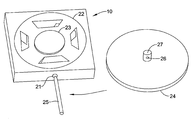
- FIG. 5 is a diagram of structure 10 shown with a seal 22 on the surface near an outer or peripheral portion so as to hermetically contain a mirror within another structure such as a cavity. The seal could, in some instances, be on the outside edge of structure 10 .
- FIG. 6 is a diagram of structure 10 in FIG. 5 but additionally having a dielectric mirror 23 formed or deposited on the surface of the inner or center portion of structure 10 .
- FIG. 7 is a diagram of structure 10 with gaps and resulting supports 29 , e.g., legs, links, adapted or etched, and a hole 28 for attaching an actuator such as piezo electric driver on structure 10 .
- FIG. 8 is a diagram of components for implementing an actuation mechanism for structure 10 .
- Component 24 is an actuator such as, for example, a piezo electric driver.
- Component 25 is a pin or like item that may be placed in hole 21 of structure 10 and hole 26 of a shaft or pin 27 attached to the actuator or driver 24 .
- FIG. 9 is a diagram of the side of structure 10 upon where the actuator or driver 24 may be attached with short pin or shaft 27 inserted into a hole 28 of structure 10 . Etched gaps with resulting thin supports 29 for center portion of structure 10 are shown on the actuator side.
- FIG. 10 is a diagram of the mirror side of structure 10 with the actuator or driver 24 attached to structure 10 and held in with pin 25 inserted through hole 21 of structure 10 and hole 26 of pin or shaft 27 of actuator or driver 24 . Glue may be applied to pin 25 and/or hole 21 for sealing to prevent gas from escaping from the cavity through any portions of hole 21 .
- An indication 37 may show a direction of mirror 23 motion relative to the perimeter of structure 10 such as at the seal 22 .
- Line 39 may provide control of actuator 24 which is for providing the motion according to indication 37 to mirror 23 .
- the motion of mirror 23 may be for adjustment of mirror position.
- FIG. 11 is a diagram with a mirror end view of the transducer mirror structure 10 and driver or actuator 24 , such as a piezo electric driver, which are attachable to each other without a side pin-like item 25 like that in FIG. 10 , to hold the actuator 24 in place relative to the transducer mirror structure 10 .
- FIG. 12 is a diagram with actuator 24 end view of the structure of FIG. 11 .
- the main attachment may be the pin or shaft 27 in FIG. 11 on the actuator 24 being glued to the back of the silicon transducer mirror structure 10 , where pin or shaft 27 fit into hole 28 in structure 10 as shown in FIG. 12 .
- Actuator 24 may be sealed to the backside of structure 10 so that any gas would not escape from the cavity through the structure 10 openings.
- the front side of the cavity may be sealed to the structure around the periphery.
- the external perimeter of structure 10 might be circular rather than a square cut. Hole 28 may be etched in the silicon structure 10 at the same time that the other openings are
- FIG. 13 is a flow diagram of a fabrication process of the transducer structure 10 .
- Step 31 may be obtaining a silicon piece, block or substrate for structure 10 which may be etched to form gaps, slots, links, legs or supports 29 to hold a center portion 35 relative to an outer portion 36 .
- Step 32 may include a straight RIE etch for making, for instance, gaps for the flexible supports 29 .
- Step 33 may include a second etch which is a KOH under etch for further making the supports 29 .
- Step 34 may include making a hole 28 for holding an actuator. Gaps, slots, links, legs and supports 29 , and the like, may be of various shapes.
- Other steps may include adding a mirror 23 and a seal 22 as described herein, and attaching resultant structure 10 to another structure 38 shown in FIG. 14 , such as a cavity of a cavity ring-down spectroscopy system.
Landscapes
- Physics & Mathematics (AREA)
- General Physics & Mathematics (AREA)
- Optics & Photonics (AREA)
- Health & Medical Sciences (AREA)
- Life Sciences & Earth Sciences (AREA)
- Chemical & Material Sciences (AREA)
- Analytical Chemistry (AREA)
- Biochemistry (AREA)
- General Health & Medical Sciences (AREA)
- Immunology (AREA)
- Pathology (AREA)
- Micromachines (AREA)
Abstract
Description
Claims (8)
Priority Applications (1)
| Application Number | Priority Date | Filing Date | Title |
|---|---|---|---|
| US12/144,382 US8218215B2 (en) | 2008-06-23 | 2008-06-23 | Transducer-mirror structure |
Applications Claiming Priority (1)
| Application Number | Priority Date | Filing Date | Title |
|---|---|---|---|
| US12/144,382 US8218215B2 (en) | 2008-06-23 | 2008-06-23 | Transducer-mirror structure |
Publications (2)
| Publication Number | Publication Date |
|---|---|
| US20090316245A1 US20090316245A1 (en) | 2009-12-24 |
| US8218215B2 true US8218215B2 (en) | 2012-07-10 |
Family
ID=41430974
Family Applications (1)
| Application Number | Title | Priority Date | Filing Date |
|---|---|---|---|
| US12/144,382 Expired - Fee Related US8218215B2 (en) | 2008-06-23 | 2008-06-23 | Transducer-mirror structure |
Country Status (1)
| Country | Link |
|---|---|
| US (1) | US8218215B2 (en) |
Citations (9)
| Publication number | Priority date | Publication date | Assignee | Title |
|---|---|---|---|---|
| US5311280A (en) | 1983-07-21 | 1994-05-10 | Kearfott Guidance & Navigation Corporation | Laser light length control assembly for ring laser gyro |
| US5832017A (en) | 1996-03-15 | 1998-11-03 | Motorola Inc | Reliable near IR VCSEL |
| US5912740A (en) | 1997-06-20 | 1999-06-15 | The Board Of Trustees Of The Leland Stanford Junior University | Ring resonant cavities for spectroscopy |
| US20020131679A1 (en) * | 2001-02-07 | 2002-09-19 | Nasiri Steven S. | Microelectromechanical mirror and mirror array |
| US20050035699A1 (en) * | 2003-08-15 | 2005-02-17 | Hsiung-Kuang Tsai | Optical interference display panel |
| US20050046980A1 (en) * | 2002-06-11 | 2005-03-03 | Fujitsu Limited | Micro mirror unit and method of making the same |
| US7145165B2 (en) | 2001-09-12 | 2006-12-05 | Honeywell International Inc. | Tunable laser fluid sensor |
| US20070139752A1 (en) * | 2005-12-16 | 2007-06-21 | The Charles Stark Draper Laboratory, Inc. | Systems, methods and devices for actuating a moveable miniature platform |
| US7807061B2 (en) * | 2006-07-19 | 2010-10-05 | Denso Corporation | Optical gas concentration detector and method of producing structure used in the detector |
-
2008
- 2008-06-23 US US12/144,382 patent/US8218215B2/en not_active Expired - Fee Related
Patent Citations (9)
| Publication number | Priority date | Publication date | Assignee | Title |
|---|---|---|---|---|
| US5311280A (en) | 1983-07-21 | 1994-05-10 | Kearfott Guidance & Navigation Corporation | Laser light length control assembly for ring laser gyro |
| US5832017A (en) | 1996-03-15 | 1998-11-03 | Motorola Inc | Reliable near IR VCSEL |
| US5912740A (en) | 1997-06-20 | 1999-06-15 | The Board Of Trustees Of The Leland Stanford Junior University | Ring resonant cavities for spectroscopy |
| US20020131679A1 (en) * | 2001-02-07 | 2002-09-19 | Nasiri Steven S. | Microelectromechanical mirror and mirror array |
| US7145165B2 (en) | 2001-09-12 | 2006-12-05 | Honeywell International Inc. | Tunable laser fluid sensor |
| US20050046980A1 (en) * | 2002-06-11 | 2005-03-03 | Fujitsu Limited | Micro mirror unit and method of making the same |
| US20050035699A1 (en) * | 2003-08-15 | 2005-02-17 | Hsiung-Kuang Tsai | Optical interference display panel |
| US20070139752A1 (en) * | 2005-12-16 | 2007-06-21 | The Charles Stark Draper Laboratory, Inc. | Systems, methods and devices for actuating a moveable miniature platform |
| US7807061B2 (en) * | 2006-07-19 | 2010-10-05 | Denso Corporation | Optical gas concentration detector and method of producing structure used in the detector |
Also Published As
| Publication number | Publication date |
|---|---|
| US20090316245A1 (en) | 2009-12-24 |
Similar Documents
| Publication | Publication Date | Title |
|---|---|---|
| CN102576149B (en) | For the actuator of mobile micro mechanical organ | |
| US7054011B2 (en) | Optical fiber pressure and acceleration sensor fabricated on a fiber endface | |
| US8201452B2 (en) | Housing for micro-mechanical and micro-optical components used in mobile applications | |
| CA2793452C (en) | Optical-fiber-compatible acoustic sensor | |
| EP1155297B1 (en) | Resonant sensor | |
| US6894787B2 (en) | Optical pressure sensor | |
| JP4603489B2 (en) | Tunable filter | |
| US20080277672A1 (en) | Lid structure for microdevice and method of manufacture | |
| EP1078227B1 (en) | An optically addressed sensing system | |
| US8878316B2 (en) | Cap side bonding structure for backside absolute pressure sensors | |
| US6914871B2 (en) | Micro mirror unit, optical disc drive using same, and method for producing micro mirror unit | |
| JP2005043351A (en) | Micro machining type pressure sensor | |
| US8218215B2 (en) | Transducer-mirror structure | |
| Parkes et al. | Design and fabrication of dielectric diaphragm pressure sensors for applications to shock wave measurement in air | |
| JP2000035369A (en) | Pressure sensor and its manufacturing method | |
| JP2005227282A (en) | Manufacturing method of micromechanical sensor for detecting value representing pressure and micromechanical sensor for detecting value representing pressure | |
| Agarwal et al. | Fabrication of integrated vertical mirror surfaces and transparent window for packaging MEMS devices | |
| EP0997721B1 (en) | Pressure sensor and a method of manufacturing the same | |
| WO2024200430A1 (en) | Membrane assembly with protective screen as damper | |
| Lutzenberger et al. | Large area molded silicon nitride micro mirrors | |
| JPH116779A (en) | Pressure sensor | |
| JPH08292113A (en) | Pressure sensor and manufacturing method thereof | |
| JPH08201195A (en) | Pressure sensor and manufacturing method thereof | |
| JPH02143114A (en) | Optical sensor |
Legal Events
| Date | Code | Title | Description |
|---|---|---|---|
| AS | Assignment |
Owner name: HONEYWELL INTERNATIONAL INC., NEW JERSEY Free format text: ASSIGNMENT OF ASSIGNORS INTEREST;ASSIGNOR:COLE, BARRETT E.;REEL/FRAME:021136/0979 Effective date: 20080619 |
|
| ZAAA | Notice of allowance and fees due |
Free format text: ORIGINAL CODE: NOA |
|
| ZAAB | Notice of allowance mailed |
Free format text: ORIGINAL CODE: MN/=. |
|
| STCF | Information on status: patent grant |
Free format text: PATENTED CASE |
|
| FPAY | Fee payment |
Year of fee payment: 4 |
|
| MAFP | Maintenance fee payment |
Free format text: PAYMENT OF MAINTENANCE FEE, 8TH YEAR, LARGE ENTITY (ORIGINAL EVENT CODE: M1552); ENTITY STATUS OF PATENT OWNER: LARGE ENTITY Year of fee payment: 8 |
|
| FEPP | Fee payment procedure |
Free format text: MAINTENANCE FEE REMINDER MAILED (ORIGINAL EVENT CODE: REM.); ENTITY STATUS OF PATENT OWNER: LARGE ENTITY |
|
| LAPS | Lapse for failure to pay maintenance fees |
Free format text: PATENT EXPIRED FOR FAILURE TO PAY MAINTENANCE FEES (ORIGINAL EVENT CODE: EXP.); ENTITY STATUS OF PATENT OWNER: LARGE ENTITY |
|
| STCH | Information on status: patent discontinuation |
Free format text: PATENT EXPIRED DUE TO NONPAYMENT OF MAINTENANCE FEES UNDER 37 CFR 1.362 |
|
| FP | Lapsed due to failure to pay maintenance fee |
Effective date: 20240710 |